Graphene
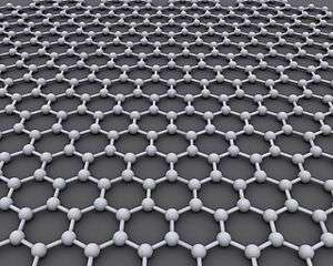
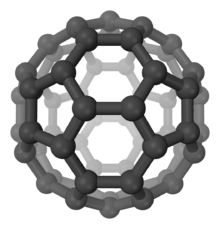
Graphene is a semimetal with small overlap between the valence and the conduction bands (zero bandgap material).[1] It is an allotrope (form) of carbon consisting of a single layer of carbon atoms arranged in a hexagonal lattice.[2][3] It is the basic structural element of many other allotropes of carbon, such as graphite, diamond, charcoal, carbon nanotubes and fullerenes.
It can be considered as an indefinitely large aromatic molecule, the ultimate case of the family of flat polycyclic aromatic hydrocarbons.[4]
Graphene has many uncommon properties. It is the strongest material ever tested, conducts heat and electricity efficiently, and is nearly transparent. Graphene shows a large and nonlinear diamagnetism,[5] greater than that of graphite, and can be levitated by neodymium magnets.
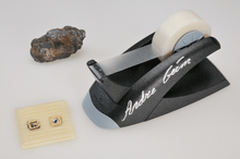
Scientists theorized about graphene for years. It had been produced unintentionally in small quantities for centuries through the use of pencils and other similar graphite applications. It was observed originally in electron microscopes in 1962, but it was studied only while supported on metal surfaces.[6] The material was later rediscovered, isolated, and characterized in 2004 by Andre Geim and Konstantin Novoselov at the University of Manchester.[7][8] Research was informed by existing theoretical descriptions of its composition, structure, and properties.[9] This work resulted in the two winning the Nobel Prize in Physics in 2010 "for groundbreaking experiments regarding the two-dimensional material graphene."[10]
Definition
"Graphene" is a combination of "graphite" and the suffix -ene, named by Hanns-Peter Boehm and colleagues,[11] who produced and observed single-layer carbon foils in 1962.[6]
Boehm et al. introduced the term graphene in 1986 to describe single sheets of graphite. Graphene can be considered an "infinite alternant" (only six-member carbon ring) polycyclic aromatic hydrocarbon.[12]
The International Union of Pure and Applied Chemistry (IUPAC) notes, "previously, descriptions such as graphite layers, carbon layers, or carbon sheets have been used for the term graphene...it is incorrect to use for a single layer a term which includes the term graphite, which would imply a three-dimensional structure. The term graphene should be used only when the reactions, structural relations or other properties of individual layers are discussed."[4]
Geim defined "isolated or free-standing graphene" as "graphene is a single atomic plane of graphite, which – and this is essential – is sufficiently isolated from its environment to be considered free-standing."[13] This definition is narrower than the IUPAC definition and refers to cloven, transferred and suspended graphene. Other forms such as graphene grown on various metals, can become free-standing if, for example, suspended or transferred [14][15] to silicon dioxide (SiO
2) or silicon carbide.[16]
Structure
Graphene is a crystalline allotrope of carbon with 2-dimensional properties. Its carbon atoms are packed densely in a regular atomic-scale chicken wire (hexagonal) pattern.[17]
Each atom has four bonds: one σ bond with each of its three neighbors and one π-bond that is oriented out of plane. The atoms are about 1.42 Å apart.[17]
Graphene's hexagonal lattice can be regarded as two interleaving triangular lattices. This perspective was successfully used to calculate the band structure for a single graphite layer using a tight-binding approximation.[17]
Graphene's stability is due to its tightly packed carbon atoms and a sp2 orbital hybridization – a combination of orbitals s, px and py that constitute the σ-bond. The final pz electron makes up the π-bond. The π-bonds hybridize together to form the π-band and π∗-bands. These bands are responsible for most of graphene's notable electronic properties, via the half-filled band that permits free-moving electrons.[17]
Graphene sheets in solid form usually show evidence in diffraction for graphite's (002) layering. This is true of some single-walled nanostructures.[18] However, unlayered graphene with only (hk0) rings has been found in the core of presolar graphite onions.[19] TEM studies show faceting at defects in flat graphene sheets[20] and suggest a role for two-dimensional crystallization from a melt.
Graphene can self-repair holes in its sheets when exposed to molecules containing carbon, such as hydrocarbons. Bombarded with pure carbon atoms, the atoms perfectly align into hexagons, completely filling the holes.[21][22]
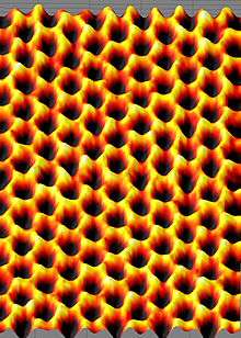
The atomic structure of isolated, single-layer graphene was studied by TEM on sheets of graphene suspended between bars of a metallic grid.[23] Electron diffraction patterns showed the expected honeycomb lattice. Suspended graphene showed "rippling" of the flat sheet, with amplitude of about one nanometer. These ripples may be intrinsic to the material as a result of the instability of two-dimensional crystals,[24][25][26] or may originate from the ubiquitous dirt seen in all TEM images of graphene. Atomic resolution real-space images of isolated, single-layer graphene on SiO
2 substrates are available[27] via scanning tunneling microscopy (STM). Photoresist residue, which must be removed to obtain atomic-resolution images, may be the "adsorbates" observed in TEM images, and may explain the observed rippling. Rippling on SiO
2 is caused by conformation of graphene to the underlying SiO
2 and is not intrinsic.[27]
Stability
Ab initio calculations show that a graphene sheet is thermodynamically unstable if its size is less than about 20 nm ("graphene is the least stable structure until about 6000 atoms") and becomes the most stable fullerene (as within graphite) only for molecules larger than 24,000 atoms.[28]
Analogs
Analogs[29] (also referred to as "artificial graphene") are two-dimensional systems that exhibit similar properties to graphene. Analogs can be systems in which the physics is easier to observe and to manipulate. In those systems, electrons are not always the chosen particles—they might be optical photons,[30] microwave photons,[31] plasmons,[32] microcavity polaritons[33] or even atoms.[34] Also, the honeycomb structure in which those particles evolve can be of a different nature than carbon atoms in graphene. It can be, respectively, a photonic crystal, an array of metallic rods, metallic nanoparticles, a lattice of coupled microcavities or an optical lattice.
Properties
Graphene has a theoretical specific surface area (SSA) of 2630 m2/g. This is much larger than that reported to date for carbon black (typically smaller than 900 m2/g) or for carbon nanotubes (CNTs), from ≈100 to 1000 m2/g and is similar to activated carbon.[35]
Electronic
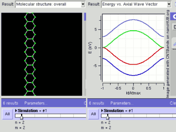
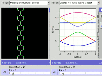
Graphene is a zero-gap semiconductor, because its conduction and valence bands meet at the Dirac points, which are six locations in momentum space, on the edge of the Brillouin zone, divided into two non-equivalent sets of three points. The two sets are labeled K and K'. The sets give graphene a valley degeneracy of gv = 2. By contrast, for traditional semiconductors the primary point of interest is generally Γ, where momentum is zero.[17] However, if the in-plane direction is confined, in which case it is referred to as a nanoribbon, its electronic structure is different. If it is "zig-zag", the bandgap is zero. If it is "armchair", the bandgap is non-zero (see figure).
Graphene displays remarkable electron mobility at room temperature, with reported values in excess of 15000 cm2⋅V−1⋅s−1.[24] Hole and electron mobilities were expected to be nearly identical.[36] The mobility is nearly independent of temperature between 10 K and 100 K,[37][38][39] which implies that the dominant scattering mechanism is defect scattering. Scattering by graphene's acoustic phonons intrinsically limits room temperature mobility to 200000 cm2⋅V−1⋅s−1 at a carrier density of 1012 cm−2,[39][40] 4.5×10³ times greater than copper.[41][42]
The corresponding resistivity of graphene sheets would be 10−6 Ω⋅cm. This is less than the resistivity of silver, the lowest otherwise known at room temperature.[43] However, on SiO
2 substrates, scattering of electrons by optical phonons of the substrate is a larger effect than scattering by graphene’s own phonons. This limits mobility to 40000 cm2⋅V−1⋅s−1.[39] Charge transport is affected by adsorption of contaminants such as water and oxygen molecules. This leads to non-repetitive and large hysteresis I-V characteristics.
Electrons propagating through graphene's honeycomb lattice effectively lose their mass, producing quasi-particles that are described by a 2D analogue of the Dirac equation rather than the Schrödinger equation for spin-1⁄2 particles.[44][36]
Superconductivity has been observed in twisted bilayer graphene [45].
Optical
Graphene's unique optical properties produce an unexpectedly high opacity for an atomic monolayer in vacuum, absorbing πα ≈ 2.3% of red light, where α is the fine-structure constant.[48] This is a consequence of the "unusual low-energy electronic structure of monolayer graphene that features electron and hole conical bands meeting each other at the Dirac point... [which] is qualitatively different from more common quadratic massive bands."[47] Based on the Slonczewski–Weiss–McClure (SWMcC) band model of graphite, the interatomic distance, hopping value and frequency cancel when optical conductance is calculated using Fresnel equations in the thin-film limit.
Although confirmed experimentally, the measurement is not precise enough to improve on other techniques for determining the fine-structure constant.[49]
Multi-parametric surface plasmon resonance was used to characterize both thickness and refractive index of chemical-vapor-deposition (CVD)-grown graphene films. The measured refractive index and extinction coefficient values at 670 nm wavelength are 3.135 and 0.897, respectively. The thickness was determined as 3.7 Å from a 0.5 mm area, which agrees with 3.35 Å reported for layer-to-layer carbon atom distance of graphite crystals.[50]
The method can be used for real-time label-free interactions of graphene with organic and inorganic substances. The existence of unidirectional surface plasmons in the nonreciprocal graphene-based gyrotropic interfaces has been demonstrated theoretically. By efficiently controlling the chemical potential of graphene, the unidirectional working frequency can be continuously tunable from THz to near-infrared and even visible.[51] Particularly, the unidirectional frequency bandwidth can be 1–2 orders of magnitude larger than that in metal under the same magnetic field, which arises from the superiority of extremely small effective electron mass in graphene.
Graphene's band gap can be tuned from 0 to 0.25 eV (about 5 micrometre wavelength) by applying voltage to a dual-gate bilayer graphene field-effect transistor (FET) at room temperature.[52] The optical response of graphene nanoribbons is tunable into the terahertz regime by an applied magnetic field.[53] Graphene/graphene oxide systems exhibit electrochromic behavior, allowing tuning of both linear and ultrafast optical properties.[54]
A graphene-based Bragg grating (one-dimensional photonic crystal) demonstrated its capability for excitation of surface electromagnetic waves in the periodic structure using a 633 nm He–Ne laser as the light source.[55]
Saturable absorption
Such unique absorption could become saturated when the input optical intensity is above a threshold value. This nonlinear optical behavior is termed saturable absorption and the threshold value is called the saturation fluence. Graphene can be saturated readily under strong excitation over the visible to near-infrared region, due to the universal optical absorption and zero band gap. This has relevance for the mode locking of fiber lasers, where fullband mode locking has been achieved by a graphene-based saturable absorber. Due to this special property, graphene has wide application in ultrafast photonics. The optical response of graphene/graphene oxide layers can be tuned electrically.[54][56] Saturable absorption in graphene could occur at the Microwave and Terahertz bands, owing to its wideband optical absorption property. The microwave saturable absorption in graphene demonstrates the possibility of graphene microwave and terahertz photonics devices, such as a microwave saturable absorber, modulator, polarizer, microwave signal processing and broad-band wireless access networks.[57]
Nonlinear Kerr effect
Under more intensive laser illumination, graphene could possess a nonlinear phase shift due to the optical nonlinear Kerr effect. Based on a typical open and close aperture z-scan measurement, graphene possesses a nonlinear Kerr coefficient of 10−7 cm2⋅W−1, almost nine orders of magnitude larger than that of bulk dielectrics.[58] This suggests that graphene may be a powerful nonlinear Kerr medium, with the possibility of observing a variety of nonlinear effects, the most important of which is the soliton.[59] A 2016 study has shown that the nonlinear refractive index of graphene is negative.[60] Thermal lens spectroscopy can be used for measuring the thermo-optic coefficient of graphene and inspecting its thermal nonlinearity.[61]
Quantum dots
Several techniques can prepare nanostructured graphene, e.g., graphene quantum dots (GQDs); these techniques mainly include electron beam lithography, chemical synthesis, electrochemical preparation, graphene oxide (GO) reduction, C60 catalytic transformation, the microwave assisted hydrothermal method (MAH),[62][63] the Soft-Template method,[64] the hydrothermal method,[65][66][67] and the ultrasonic exfoliation method.[68]
Thermal
Thermal conductivity
Thermal transport in graphene is an active area of research which has attracted attention because of the potential for thermal management applications. Early measurements of the thermal conductivity of suspended graphene reported an exceptionally large thermal conductivity of approximately 5300 W⋅m−1⋅K−1,[69] compared with the thermal conductivity of pyrolytic graphite of approximately 2000 W⋅m−1⋅K−1 at room temperature.[70] However, later studies have questioned whether this ultrahigh value was overestimated, and instead measured thermal conductivities between 1500–2500 W⋅m−1⋅K−1 for suspended single layer graphene.[71][72][73][74][75] The large range can be attributed to large measurement uncertainties as well as variations in the graphene quality and processing conditions. In addition, when single-layer graphene is supported on an amorphous material, the thermal conductivity is reduced to about 500–600 W⋅m−1⋅K−1 at room temperature as a result of scattering of graphene lattice waves by the substrate,[76][77] and can be even lower for few layer graphene encased in amorphous oxide.[78] Likewise, polymeric residue can contribute to a similar decrease for suspended graphene to approximately 500–600 W⋅m−1⋅K−1for bilayer graphene.[79]
It has been suggested that the isotopic composition, the ratio of 12C to 13C, has a significant impact on thermal conductivity. For example, isotopically pure 12C graphene has higher thermal conductivity than either a 50:50 isotope ratio or the naturally occurring 99:1 ratio.[80] It can be shown by using the Wiedemann–Franz law, that the thermal conduction is phonon-dominated.[69] However, for a gated graphene strip, an applied gate bias causing a Fermi energy shift much larger than kBT can cause the electronic contribution to increase and dominate over the phonon contribution at low temperatures. The ballistic thermal conductance of graphene is isotropic.[81][82]
Potential for this high conductivity can be seen by considering graphite, a 3D version of graphene that has basal plane thermal conductivity of over 1000 W⋅m−1⋅K−1 (comparable to diamond). In graphite, the c-axis (out of plane) thermal conductivity is over a factor of ≈100 smaller due to the weak binding forces between basal planes as well as the larger lattice spacing.[83] In addition, the ballistic thermal conductance of graphene gives the lower limit of the ballistic thermal conductances, per unit circumference and length of carbon nanotubes.[84]
Despite its 2-D nature, graphene has 3 acoustic phonon modes. The two in-plane modes (LA, TA) have a linear dispersion relation, while the out of plane mode (ZA) has a quadratic dispersion relation. Due to this, the T2 dependent thermal conductivity contribution of the linear modes is dominated at low temperatures by the T1.5 contribution of the out-of-plane mode.[84] Some graphene phonon bands display negative Grüneisen parameters (GPs).[85] At low temperatures (where most optical modes with positive GPs are still not excited) the contribution from the negative GPs will be dominant and thermal expansion coefficient (which is directly proportional to GPs) negative. The lowest negative GPs correspond to the lowest transverse acoustic ZA modes. Phonon frequencies for such modes increase with the in-plane lattice parameter since atoms in the layer upon stretching will be less free to move in the z direction. This is similar to the behavior of a stretched string that has vibrations of smaller amplitude and higher frequency. This phenomenon, named "membrane effect", was predicted by Lifshitz in 1952.[86]
Melting point
A prediction that was published in 2015 suggested a melting point of ≈4125 K.[87] Recent and more sophisticated modelling has increased this temperature to at least 5000 K. At 6000 K (the sun's surface having an effective temperature of 5,777 K)[88] graphene melts into an agglomeration of loosely coupled doubled bonded chains, before becoming a gas.[89]
Mechanical
The carbon–carbon bond length in graphene is about 0.142 nanometers.[90] Graphene sheets stack to form graphite with an interplanar spacing of 0.335 nm.
Graphene is the strongest material ever tested,[91] with an intrinsic tensile strength of 130.5 GPa and a Young's modulus of 1 TPa (150000000 psi).[91] The Nobel announcement gave the strength as 42 N/m; the mass of 1 m2 as 0.77 mg, and the electrical resistance of a square as 31 Ω.[92]
Large-angle-bent graphene monolayer has been achieved with negligible strain, showing mechanical robustness of the two-dimensional carbon nanostructure. Even with extreme deformation, excellent carrier mobility in monolayer graphene can be preserved.[93]
The spring constant of suspended graphene sheets has been measured using an atomic force microscope (AFM).[91][94] Graphene sheets were suspended over SiO
2 cavities where an atomic force microscope (AFM) tip was used to apply a stress to the sheet to test its mechanical properties. Its spring constant was in the range 1–5 N/m and the stiffness was 0.5 TPa, which differs from that of bulk graphite. These intrinsic properties could lead to applications such as NEMS as pressure sensors and resonators.[95] Due to its large surface energy and out of plane ductility, flat graphene sheets are unstable with respect to scrolling, i.e. bending into a cylindrical shape, which is its lower-energy state.[96]
As is true of all materials, regions of graphene are subject to thermal and quantum fluctuations in relative displacement. Although the amplitude of these fluctuations is bounded in 3D structures (even in the limit of infinite size), the Mermin–Wagner theorem shows that the amplitude of long-wavelength fluctuations grows logarithmically with the scale of a 2D structure and would therefore be unbounded in structures of infinite size.[97][98] Local deformation and elastic strain are negligibly affected by this long-range divergence in relative displacement. It is believed that a sufficiently large 2D structure, in the absence of applied lateral tension, will bend and crumple to form a fluctuating 3D structure. Ripples have been observed in suspended layers of graphene.[23] It has been proposed that the ripples are caused by thermal fluctuations in the material. As a consequence of these dynamical deformations, it is debatable whether graphene is truly a 2D structure.[24][25][26][99] In 2014 it was shown that these ripples, if amplified through the introduction of vacancy defects, can impart a negative Poisson's ratio into graphene, resulting in the thinnest auxetic material known.[100]
Graphene nanosheets can be incorporated into a nickel matrix through a plating process to form Ni-graphene composites on a target substrate. The enhancement in mechanical properties of the composites is attributed to the high interaction between Ni and graphene and the prevention of the dislocation sliding in the Ni matrix by the graphene.[101]
Fracture toughness
Despite its strength, graphene is also relatively brittle, with a fracture toughness of about 4 MPa√m.[102] This indicates that imperfect graphene is likely to crack in a brittle manner like ceramic materials, as opposed to many metallic materials that have fracture toughnesses in the range of 15–50 MPa√m. Graphene shows a greater ability to distribute force from an impact than any known material, ten times that of steel per unit weight.[103] The force was transmitted at 22.2 kilometres per second (13.8 mi/s).[104]
Biological
In 2011 graphene was shown to accelerate the osteogenic differentiation of human mesenchymal stem cells without the use of biochemical inducers.[105]
In 2015 graphene was used to create biosensors with epitaxial graphene on silicon carbide. The sensors bind to 8-hydroxydeoxyguanosine (8-OHdG) and is capable of selective binding with antibodies. The presence of 8-OHdG in blood, urine and saliva is commonly associated with DNA damage. Elevated levels of 8-OHdG have been linked to increased risk of several cancers.[106] A commercial version of a graphene biosensor has been used as a protein binding sensor platform.[107]
In 2016 uncoated graphene was shown to serve as a neuro-interface electrode without altering or damaging properties such as signal strength or formation of scar tissue. Graphene electrodes in the body stay significantly more stable than electrodes of tungsten or silicon because of properties such as flexibility, bio-compatibility and conductivity.[108]
Forms
A production unit produces continuous monolayer sheets of high-strength monolayer graphene (HSMG).[109] The process is based on graphene growth on a liquid metal matrix.[110]
Bilayer graphene displays the anomalous quantum Hall effect, a tunable band gap[111] and potential for excitonic condensation.[112] Bilayer graphene typically can be found either in twisted configurations where the two layers are rotated relative to each other or graphitic Bernal stacked configurations where half the atoms in one layer lie atop half the atoms in the other.[113] Stacking order and orientation govern its optical and electronic properties. One synthesis method is chemical vapor deposition, which can produce large bilayer regions that almost exclusively conform to a Bernal stack geometry.[113] Superconductivity has been observed in twisted bilayer graphene.
Graphene nanoribbons ("nanostripes" in the "zig-zag" orientation), at low temperatures, show spin-polarized metallic edge currents, which suggest spintronics applications. (In the "armchair" orientation, the edges behave like semiconductors.[44])
In 2013, a three-dimensional honeycomb of hexagonally arranged carbon was termed 3D graphene. Self-supporting 3D graphene was produced that year.[114] The discovered nanostructure is a multilayer system of parallel hollow nanochannels located along the surface that displayed quadrangular cross-section. Three dimensional bilayer graphene was reported in 2012[115] and 2014.[116] In 2017, freestanding graphene gyroids with 35 nm and 60 nm unit cells were fabricated via controlled direct chemical vapor deposition. They represent the smallest free standing periodic graphene 3D structures yet produced with a pore size of tens of nm.[117] A graphene gyroid has five percent of the density of steel, yet is ten times as strong with an enormous surface area to volume ratio.[118][119] An aerogel made of graphene layers separated by carbon nanotubes was measured at 0.16 milligrams per cubic centimeter. The material has superior elasticity and absorption: it can recover completely after more than 90% compression, and absorb up to 900 times its weight in oil, at a rate of 68.8 grams per second.[120]
Production
Multiple production techniques have been developed. Isolated 2D crystals cannot be grown via chemical synthesis beyond small sizes even in principle, because the rapid growth of phonon density with increasing lateral size forces 2D crystallites to bend into the third dimension.[13] In all cases, graphene must bond to a substrate to retain its two-dimensional shape.[13]
As of 2014, exfoliation produced graphene with the lowest number of defects and highest electron mobility.[42] Geim and Novoselov initially used adhesive tape to pull graphene sheets away from graphite. Achieving single layers typically requires multiple exfoliation steps. After exfoliation the flakes are deposited on a silicon wafer. Alternatively a sharp single-crystal diamond wedge cleave layers from a graphite source.[121] Another method is reduction of graphite oxide monolayer films, e.g. by hydrazine with annealing in argon/hydrogen with an almost intact carbon framework that allows efficient removal of functional groups. Measured charge carrier mobility exceeded 1,000 centimetres (393.70 in)/Vs.[122] Defect-free, unoxidized graphene-containing liquids can be made from graphite using mixers that produce local shear rates greater than 10×104.[123][124] Burning a graphite oxide coated DVD produced a conductive graphene film (1738 siemens per meter) and specific surface area (1520 square meters per gram) that was highly resistant and malleable.[125]
Dispersing graphite in a liquid medium can produce graphene by sonication followed by centrifugation.[126] The addition of dispersants (e.g., graphene quantum dots) can facilitate the exfoliation process, forming aqueous graphene dispersion with high yield.[127] Such process is straightforward, low-cost, and environmentally friendly. Sonicating graphite at the interface of two immiscible liquids, most notably heptane and water, produced macro-scale graphene films.[128] Graphite particles can be corroded in molten salts to form a variety of carbon nanostructures including graphene.[129] Electrochemical synthesis can exfoliate graphene. Varying a pulsed voltage controls thickness, flake area, number of defects and affects its properties. The process begins by bathing the graphite in a solvent for intercalation. The process can be tracked by monitoring the solution’s transparency with an LED and photodiode. [130][131]
Graphene has been prepared by using a sugar (e.g. glucose, sugar, fructose, etc.) This substrate-free "bottom-up" synthesis is safer, simpler and more environmentally friendly than exfoliation. The method can control thickness, ranging from monolayer to multilayers, which is known as "Tang-Lau Method".[132]
Epitaxial graphene may be coupled to surfaces weakly enough (by Van der Waals forces) to retain the two dimensional electronic band structure of isolated graphene.[133] Heating silicon carbide (SiC) to high temperatures (1100 °C) under low pressures (c. 10−6 torr) reduces it to graphene.[134][135][136][137][138][139] A normal silicon wafer coated with a layer of germanium (Ge) dipped in dilute hydrofluoric acid strips the naturally forming germanium oxide groups, creating hydrogen-terminated germanium. CVD can coat that with graphene.[140][141] A two-step CVD process is shown to grow graphene directly on TiO2 crystals or exfoliated TiO2 nanosheets without using a metal catalyst.[142] The atomic structure of metal substrates including ruthenium,[143] iridium,[144] nickel[145] and copper has been used as substrates for graphene production.[146] Commercial copper foils have been used for graphene production, reducing substrate costs by 100-fold.[147][15] Gaseous catalyst-assisted CVD [148] paves the way for synthesizing high-quality graphene for device applications while avoiding the transfer process. Gram quantities were produced by the reduction of ethanol by sodium metal, followed by pyrolysis and washing with water.[149] Growing graphene in an industrial resistive-heating cold wall CVD system was claimed to produce graphene 100 times faster than conventional CVD systems, cut costs by 99% and produce material with enhanced electronic qualities.[150][151] Experiments with precise control of process parameters during cold wall CVD provided conclusive insight into the classical surface-mediated two dimensional nucleation and growth mechanism of graphene grown using catalytic CVD under conditions sought out in the semiconductor industry.[152][153]
In applications where the thickness and packing density of the graphene layer need to be carefully controlled, the Langmuir-Blodgett method has been used to produce single layer films of graphene and graphene oxide which can then be reduced to graphene.[154][155][156] Some of the benefits of Langmuir-Blodgett deposition include accurate control over the layered architecture of the graphene, that the layer-by-layer deposition process allows assembling any combination of thin carbon layers on a substrates, and that the assembly process is performed at room temperature and produces greater throughputs while being amenable to automation and mass production.[157]
Chemistry
Graphene is the only form of carbon (or solid material) in which every atom is available for chemical reaction from two sides (due to the 2D structure). Atoms at the edges of a graphene sheet have special chemical reactivity. Graphene has the highest ratio of edge atoms of any allotrope. Defects within a sheet increase its chemical reactivity.[158] The onset temperature of reaction between the basal plane of single-layer graphene and oxygen gas is below 260 °C (530 K).[159] Graphene combusts at 350 °C (620 K).[160] Graphene is commonly modified with oxygen- and nitrogen-containing functional groups and analyzed by infrared spectroscopy and X-ray photoelectron spectroscopy. However, determination of structures of graphene with oxygen-[161] and nitrogen-[162] functional groups requires the structures to be well controlled.
Contrary to the ideal 2D structure of graphene, chemical applications of graphene need either structural or chemical irregularities, as perfectly flat graphene is chemically inert.[163] In other words, the definition of an ideal graphene is different in chemistry and physics.
Graphene placed on a soda-lime glass (SLG) substrate under ambient conditions exhibited spontaneous n-doping (1.33 × 10¹³ e/cm2) via surface-transfer. On p-type copper indium gallium diselenide (CIGS) semiconductor itself deposited on SLG n-doping reached 2.11 × 10¹³ e/cm2.[164]
Various graphene derivatives, e.g., cyanographene and graphene acid, can be prepared via elegant chemistry of fluorographene. Cyanographene and graphene acid have high degree of functionalization (~15%), open band gap and are hydrophilic providing stable colloids in water.
Potential applications
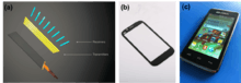
Graphene is a transparent and flexible conductor that holds promise for various material/device applications, including solar cells,[165] light-emitting diodes (LED), touch panels and smart windows or phones.[166] Graphene has also been used in other fundamental electronic devices, such as capacitors and Field Effect Transistors (FETs), in which it can act as an atomically thin channel. In the same framework, fluorine-doped graphene has shown to have insulating properties and it can be used as a passivation layer in graphene FETs, leading to a substantial increase in carrier mobility.[1]
Other early commercial uses of graphene include fillers such as a graphene-infused printer powder.[167]
Graphene supercapacitors serve as energy storage alternative to traditional electrolytic batteries. Among advantages are fast charging, long life span and environmentally friendly production. Graphene supercapacitors produced by Skeleton Technologies have been commercially available since around 2015 and were first used in some specialized applications instead of traditional batteries.[168] By 2017, commercial graphene supercapacitor units were available for industrial power applications, with maximal power output of 1500 kW.[169] In 2016, Adgero announced a regenerative braking system (KERS) for large trucks that employed a graphene-based supercapacitor.[170]
In 2016, Henrik Fisker announced development of an electric car that will use graphene supercapacitor instead of lithium-ion batteries.[171] Its low energy density as compared to lithium-ion batteries is being addressed. The planned electric car would target a minimum range of 400 miles (640 km).[171] It has been announced later that the electric car produced by Fisker Inc. will still use lithium-ion batteries, but research in graphene supercapacitors will continue by Nanotech Energy Inc.[172]
BAC's 2016 Mono model is said to be made out of graphene as a first of both a street-legal track car and a production car.[173][174] The first company to use graphene-made structural parts on a production model was Spania GTA, which unveiled a version of its Spano supercar fitted with graphene in 2015.[174][175]
The global market for graphene reached $9 million by 2012 with most sales in the semiconductor, electronics, battery, energy storage or conversion,[176] and composites industries.[177]
Health and safety
The toxicity of graphene has been extensively debated. A review on graphene toxicity summarized the in vitro, in vivo, antimicrobial and environmental effects and highlights the various mechanisms of graphene toxicity.[178] Nanotubes of graphene could reproduce the effects of asbestosis.[179][180] The toxicity of graphene depends on its shape, size, purity, post-production processing steps, oxidative state, functional groups, dispersion state, synthesis methods, route, dose of administration, and exposure times.
Graphene nanoribbons, graphene nanoplatelets, and graphene nano–onions are non-toxic at concentrations up to 50 µg/ml. These nanoparticles do not alter the differentiation of human bone marrow stem cells towards osteoblasts (bone) or adipocytes (fat) suggesting that at low doses graphene nanoparticles are safe for biomedical applications.[181] 10 µm few-layered graphene flakes were able to pierce cell membranes in solution. They were observed to enter initially via sharp and jagged points, allowing graphene to enter the cell. The physiological effects of this remain uncertain, and this remains a relatively unexplored field.[182][183]
History

The theory of graphene was first explored by Wallace in 1947 as a starting point for understanding the electronic properties of 3D graphite. The emergent massless Dirac equation was first pointed out by Semenoff, DiVincenzo and Mele.[184] The earliest TEM images of few-layer graphite were published by Ruess and Vogt in 1948.[185] An early, detailed study on few-layer graphite dates to 1962 when Boehm and colleagues reported producing monolayer flakes of reduced graphene oxide.[186][187][188][189] Efforts to make thin films of graphite by mechanical exfoliation started in 1990,[190] but nothing thinner than 50 to 100 layers was produced before 2004. Initial attempts to make atomically thin graphitic films employed exfoliation techniques similar to the drawing method. Multilayer samples down to 10 nm in thickness were obtained.[24]
One of the first patents pertaining to the production of graphene was filed in October 2002 and granted in 2006.[191] Two years later, in 2004 Geim and Novoselov extracted single-atom-thick crystallites from bulk graphite[7] and transferred them onto thin silicon dioxide (SiO
2) on a silicon wafer,[192] which electrically isolated the graphene. The cleavage technique led directly to the first observation of the anomalous quantum Hall effect in graphene,[37][193] which provided direct evidence of graphene's theoretically predicted Berry's phase of massless Dirac fermions. The effect was reported by Geim's group and by Kim and Zhang, whose papers appeared in Nature in 2005.[37][193] Geim and Novoselov received awards for their pioneering research on graphene, notably the 2010 Nobel Prize in Physics.[194]
In 2013, the European Commission funded the large-scale research project Graphene Flagship with a total budget of €1 billion, involving 150 partner organizations.
Commercialization of graphene proceeded rapidly once commercial scale production was demonstrated.[195][196][197] By 2017, 13 years after creation of the first laboratory graphene electronic device, an integrated graphene electronics chip was produced commercially and marketed to pharmaceutical researchers by Nanomedical Diagnostics in San Diego.[198]
See also
- Bilayer graphene
- Bismuthide
- Borophene
- Cadmium arsenide
- Exfoliated graphite nano-platelets
- Germanene
- Graphane
- Graphene antenna
- Graphene applications as optical lenses
- Graphene plasmonics
- Graphyne
- Metal-organic framework
- Molybdenum disulfide
- Molybdenum diselenide
- Nanoribbon
- Phagraphene
- Penta-graphene
- Silicene
- Solid-state engine
- Stanene
- Two-dimensional polymers
References
- 1 2 Ho, Kuan-I; Boutchich, Mohamed; Su, Ching-Yuan; Moreddu, Rosalia; Marianathan, Eugene Sebastian Raj; Montes, Laurent; Lai, Chao-Sung (2015). "A Self-Aligned High-Mobility Graphene Transistor: Decoupling the Channel with Fluorographene to Reduce Scattering". Advanced Materials. 27: 6519–6525. doi:10.1002/adma.201502544.
- ↑ "graphene definition, meaning – what is graphene in the British English Dictionary & Thesaurus – Cambridge Dictionaries Online". cambridge.org.
- ↑ "Graphene". Merriam-Webster.
- 1 2 "graphene layer". IUPAC Gold Book. International Union of Pure and Applied Chemistry. Retrieved 31 March 2012.
- ↑ Li, Zhilin; Chen, Lianlian; Meng, Sheng; Guo, Liwei; Huang, Jiao; Liu, Yu; Wang, Wenjun; Chen, Xiaolong (2015). "Field and temperature dependence of intrinsic diamagnetism in graphene: Theory and experiment". Phys. Rev. B. 91 (9): 094429. Bibcode:2015PhRvB..91i4429L. doi:10.1103/PhysRevB.91.094429.
- 1 2 Boehm, H. P.; Clauss, A.; Fischer, G. O.; Hofmann, U. (1 July 1962). "Das Adsorptionsverhalten sehr dünner Kohlenstoff-Folien". Zeitschrift für anorganische und allgemeine Chemie. 316 (3–4): 119–127. doi:10.1002/zaac.19623160303.
- 1 2 Novoselov, K. S.; Geim, A. K.; Morozov, S. V.; Jiang, D.; Zhang, Y.; Dubonos, S. V.; Grigorieva, I. V.; Firsov, A. A. (22 October 2004). "Electric Field Effect in Atomically Thin Carbon Films". Science. 306 (5696): 666–669. arXiv:cond-mat/0410550. Bibcode:2004Sci...306..666N. doi:10.1126/science.1102896. PMID 15499015.
- ↑ "This Month in Physics History: October 22, 2004: Discovery of Graphene". APS News. Series II. 18 (9): 2. 2009.
- ↑ "The Story of Graphene". www.graphene.manchester.ac.uk. The University of Manchester. 10 September 2014. Retrieved 9 October 2014.
- ↑ "The Nobel Prize in Physics 2010". The Nobel Foundation. Retrieved 3 December 2013.
- ↑ Boehm, H. P.; Setton, R.; Stumpp, E. (1994). "Nomenclature and terminology of graphite intercalation compounds" (PDF). Pure and Applied Chemistry. 66 (9): 1893–1901. doi:10.1351/pac199466091893. Archived from the original (PDF) on 6 April 2012.
- ↑ Simpson, C. D.; Brand, J. Diedrich; Berresheim, Alexander J.; Przybilla, Laurence; Räder, Hans Joachim; Müllen, Klaus (2002). "Synthesis of a Giant 222 Carbon Graphite Sheet". Chemistry. 8 (6): 1424–1429. doi:10.1002/1521-3765(20020315)8:6<1424::AID-CHEM1424>3.0.CO;2-Z.
- 1 2 3 Geim, A. (2009). "Graphene: Status and Prospects". Science. 324 (5934): 1530–4. arXiv:0906.3799. Bibcode:2009Sci...324.1530G. doi:10.1126/science.1158877. PMID 19541989.
- ↑ Ghoneim, Mohamed. (2012). "Nanotechnology: CVD Graphene Transfer". YouTube.
- 1 2 Ghoneim, Mohamed T.; Smith, Casey E.; Hussain, Muhammad M. (6 May 2013). "Simplistic graphene transfer process and its impact on contact resistance". Applied Physics Letters. 102 (18): 183115. Bibcode:2013ApPhL.102r3115G. doi:10.1063/1.4804642.
- ↑ Riedl, C.; Coletti, C.; Iwasaki, T.; Zakharov, A.A.; Starke, U. (2009). "Quasi-Free-Standing Epitaxial Graphene on SiC Obtained by Hydrogen Intercalation". Physical Review Letters. 103 (24): 246804. arXiv:0911.1953. Bibcode:2009PhRvL.103x6804R. doi:10.1103/PhysRevLett.103.246804. PMID 20366220.
- 1 2 3 4 5 Cooper, Daniel R.; D’Anjou, Benjamin; Ghattamaneni, Nageswara; Harack, Benjamin; Hilke, Michael; Horth, Alexandre; Majlis, Norberto; Massicotte, Mathieu; Vandsburger, Leron; Whiteway, Eric; Yu, Victor (3 November 2011). "Experimental Review of Graphene" (PDF). ISRN Condensed Matter Physics. International Scholarly Research Network. 2012: 1–56. doi:10.5402/2012/501686. Retrieved 30 August 2016.
- ↑ Kasuya, D.; Yudasaka, M.; Takahashi, K.; Kokai, F.; Iijima, S. (2002). "Selective Production of Single-Wall Carbon Nanohorn Aggregates and Their Formation Mechanism". J. Phys. Chem. B. 106 (19): 4947–4951. doi:10.1021/jp020387n.
- ↑ Bernatowicz, Thomas J; Cowsik, Ramanath; Gibbons, Patrick C; Lodders, Katharina; Fegley, Bruce; Amari, Sachiko; Lewis, Roy S (1996). "Constraints on stellar grain formation from presolar graphite in the Murchison meteorite". Astrophysical Journal. 472 (2): 760–782. Bibcode:1996ApJ...472..760B. doi:10.1086/178105.
- ↑ Fraundorf, P.; Wackenhut, M. (2002). "The core structure of presolar graphite onions". Astrophysical Journal Letters. 578 (2): L153–156. arXiv:astro-ph/0110585. Bibcode:2002ApJ...578L.153F. doi:10.1086/344633.
- ↑ Zan, Recep; Ramasse, Quentin M.; Bangert, Ursel; Novoselov, Konstantin S. (2012). "Graphene re-knits its holes". Mesoscale and Nanoscale Physics. 12 (8): 3936–3940. arXiv:1207.1487v1. Bibcode:2012NanoL..12.3936Z. doi:10.1021/nl300985q.
- ↑ Puiu, Tibi (12 July 2012). "Graphene sheets can repair themselves naturally". ZME Science.
- 1 2 3 Meyer, J.; Geim, A. K.; Katsnelson, M. I.; Novoselov, K. S.; Booth, T. J.; Roth, S. (2007). "The structure of suspended graphene sheets". Nature. 446 (7131): 60–63. arXiv:cond-mat/0701379. Bibcode:2007Natur.446...60M. doi:10.1038/nature05545. PMID 17330039.
- 1 2 3 4 Geim & Novoselov 2007.
- 1 2 Carlsson, J. M. (2007). "Graphene: Buckle or break". Nature Materials. 6 (11): 801–2. Bibcode:2007NatMa...6..801C. doi:10.1038/nmat2051. PMID 17972931.
- 1 2 Fasolino, A.; Los, J. H.; Katsnelson, M. I. (2007). "Intrinsic ripples in graphene". Nature Materials. 6 (11): 858–61. arXiv:0704.1793. Bibcode:2007NatMa...6..858F. doi:10.1038/nmat2011. PMID 17891144.
- 1 2 Ishigami, Masa; et al. (2007). "Atomic Structure of Graphene on SiO2". Nano Letters. 7 (6): 1643–1648. arXiv:0811.0587. Bibcode:2007NanoL...7.1643I. doi:10.1021/nl070613a. PMID 17497819.
- ↑ Shenderova, O. B.; Zhirnov, V. V.; Brenner, D. W. (2002). "Carbon Nanostructures". Critical Reviews in Solid State and Materials Sciences. 27 (3–4): 227–356. Bibcode:2002CRSSM..27..227S. doi:10.1080/10408430208500497.
- ↑ Polini, Marco; Guinea, Francisco; Lewenstein, Maciej; Manoharan, Hari C.; Pellegrini, Vittorio (1 September 2013). "Artificial honeycomb lattices for electrons, atoms and photons". Nature Nanotechnology. 8 (9): 625–633. arXiv:1304.0750. Bibcode:2013NatNa...8..625P. doi:10.1038/nnano.2013.161. PMID 24002076.
- ↑ Plotnik, Yonatan; Rechtsman, Mikael C.; Song, Daohong; Heinrich, Matthias; Zeuner, Julia M.; Nolte, Stefan; Lumer, Yaakov; Malkova, Natalia; Xu, Jingjun (1 January 2014). "Observation of unconventional edge states in 'photonic graphene'". Nature Materials. 13 (1): 57–62. arXiv:1210.5361. Bibcode:2014NatMa..13...57P. doi:10.1038/nmat3783. PMID 24193661.
- ↑ Bellec, Matthieu; Kuhl, Ulrich; Montambaux, Gilles; Mortessagne, Fabrice (14 January 2013). "Topological Transition of Dirac Points in a Microwave Experiment". Physical Review Letters. 110 (3): 033902. arXiv:1210.4642. Bibcode:2013PhRvL.110c3902B. doi:10.1103/PhysRevLett.110.033902. PMID 23373925.
- ↑ Scheeler, Sebastian P.; Mühlig, Stefan; Rockstuhl, Carsten; Hasan, Shakeeb Bin; Ullrich, Simon; Neubrech, Frank; Kudera, Stefan; Pacholski, Claudia (12 September 2013). "Plasmon Coupling in Self-Assembled Gold Nanoparticle-Based Honeycomb Islands". The Journal of Physical Chemistry C. 117 (36): 18634–18641. doi:10.1021/jp405560t.
- ↑ Jacqmin, T.; Carusotto, I.; Sagnes, I.; Abbarchi, M.; Solnyshkov, D. D.; Malpuech, G.; Galopin, E.; Lemaître, A.; Bloch, J. (18 March 2014). "Direct Observation of Dirac Cones and a Flatband in a Honeycomb Lattice for Polaritons". Physical Review Letters. 112 (11): 116402. arXiv:1310.8105. Bibcode:2014PhRvL.112k6402J. doi:10.1103/PhysRevLett.112.116402. PMID 24702392.
- ↑ "Spin-dependent hexagonal lattice. : Multi-component quantum gases in spin-dependent hexagonal lattices : Nature Physics : Nature Publishing Group". www.nature.com. Retrieved 26 September 2015.
- ↑ Bonaccorso, F.; Colombo, L.; Yu, G.; Stoller, M.; Tozzini, V.; Ferrari, A. C.; Ruoff, R. S.; Pellegrini, V. (2015). "Graphene, related two-dimensional crystals, and hybrid systems for energy conversion and storage". Science. 347 (6217): 1246501. Bibcode:2015Sci...347...41B. doi:10.1126/science.1246501. PMID 25554791.
- 1 2 Charlier, J.-C.; Eklund, P.C.; Zhu, J.; Ferrari, A.C. (2008). Jorio, A.; Dresselhaus and, G.; Dresselhaus, M.S., eds. Electron and Phonon Properties of Graphene: Their Relationship with Carbon Nanotubes. Carbon Nanotubes: Advanced Topics in the Synthesis, Structure, Properties and Applications. Berlin/Heidelberg: Springer-Verlag.
- 1 2 3 Novoselov, K. S.; Geim, A. K.; Morozov, S. V.; Jiang, D.; Katsnelson, M. I.; Grigorieva, I. V.; Dubonos, S. V.; Firsov, A. A. (2005). "Two-dimensional gas of massless Dirac fermions in graphene". Nature. 438 (7065): 197–200. arXiv:cond-mat/0509330. Bibcode:2005Natur.438..197N. doi:10.1038/nature04233. PMID 16281030.
- ↑ Morozov, S.V.; Novoselov, K.; Katsnelson, M.; Schedin, F.; Elias, D.; Jaszczak, J.; Geim, A. (2008). "Giant Intrinsic Carrier Mobilities in Graphene and Its Bilayer". Physical Review Letters. 100 (1): 016602. arXiv:0710.5304. Bibcode:2008PhRvL.100a6602M. doi:10.1103/PhysRevLett.100.016602. PMID 18232798.
- 1 2 3 Chen, J. H.; Jang, Chaun; Xiao, Shudong; Ishigami, Masa; Fuhrer, Michael S. (2008). "Intrinsic and Extrinsic Performance Limits of Graphene Devices on SiO
2". Nature Nanotechnology. 3 (4): 206–9. arXiv:0711.3646. doi:10.1038/nnano.2008.58. PMID 18654504. - ↑ Akturk, A.; Goldsman, N. (2008). "Electron transport and full-band electron–phonon interactions in graphene". Journal of Applied Physics. 103 (5): 053702. Bibcode:2008JAP...103e3702A. doi:10.1063/1.2890147.
- ↑ "ELECTRONIC MATERIALS" (PDF).
- 1 2 Kusmartsev, F. V.; Wu, W. M.; Pierpoint, M. P.; Yung, K. C. (2014). "Application of Graphene within Optoelectronic Devices and Transistors". arXiv:1406.0809 [cond-mat.mtrl-sci].
- ↑ Physicists Show Electrons Can Travel More Than 100 Times Faster in Graphene :: University Communications Newsdesk, University of Maryland Archived 19 September 2013 at the Wayback Machine.. Newsdesk.umd.edu (24 March 2008). Retrieved on 12 January 2014.
- 1 2 Neto, A Castro; Peres, N. M. R.; Novoselov, K. S.; Geim, A. K.; Geim, A. K. (2009). "The electronic properties of graphene" (PDF). Rev Mod Phys. 81: 109–162. arXiv:0709.1163. Bibcode:2009RvMP...81..109C. doi:10.1103/RevModPhys.81.109. Archived from the original (PDF) on 15 November 2010.
- ↑ Cao, Yuan; Fatemi, Valla; Fang, Shiang; Watanabe, Kenji; Taniguchi, Takashi; Kaxiras, Efthimios; Jarillo-Herrero, Pablo (2018-03-05). "Unconventional superconductivity in magic-angle graphene superlattices". Nature. 556 (7699): 43–50. doi:10.1038/nature26160. ISSN 0028-0836.
- ↑ Zhu, Shou-En; Yuan, Shengjun; Janssen, G. C. A. M. (1 October 2014). "Optical transmittance of multilayer graphene". EPL. 108 (1): 17007. arXiv:1409.4664. Bibcode:2014EL....10817007Z. doi:10.1209/0295-5075/108/17007.
- 1 2 Nair, R. R.; Blake, P.; Grigorenko, A. N.; Novoselov, K. S.; Booth, T. J.; Stauber, T.; Peres, N. M. R.; Geim, A. K. (6 June 2008). "Fine Structure Constant Defines Visual Transparency of Graphene". Science. 320 (5881): 1308–1308. Bibcode:2008Sci...320.1308N. doi:10.1126/science.1156965. PMID 18388259.
- ↑ Kuzmenko, A. B.; Van Heumen, E.; Carbone, F.; Van Der Marel, D. (2008). "Universal infrared conductance of graphite". Physical Review Letters. 100 (11): 117401. arXiv:0712.0835. Bibcode:2008PhRvL.100k7401K. doi:10.1103/PhysRevLett.100.117401. PMID 18517825.
- ↑ "Graphene Gazing Gives Glimpse Of Foundations Of Universe". ScienceDaily. 4 April 2008.
- ↑ Jussila, Henri; Yang, He; Granqvist, Niko; Sun, Zhipei (5 February 2016). "Surface plasmon resonance for characterization of large-area atomic-layer graphene film". Optica. 3 (2): 151–158. doi:10.1364/OPTICA.3.000151.
- ↑ Lin, Xiao; Xu, Yang; Zhang, Baile; Hao, Ran; Chen, Hongsheng; Li, Erping (2013). "Unidirectional surface plasmons in nonreciprocal graphene". New Journal of Physics. 15 (11): 113003. Bibcode:2013NJPh...15k3003L. doi:10.1088/1367-2630/15/11/113003.
- ↑ Zhang, Y.; Tang, Tsung-Ta; Girit, Caglar; Hao, Zhao; Martin, Michael C.; Zettl, Alex; Crommie, Michael F.; Shen, Y. Ron; Wang, Feng (11 June 2009). "Direct observation of a widely tunable bandgap in bilayer graphene". Nature. 459 (7248): 820–823. Bibcode:2009Natur.459..820Z. doi:10.1038/nature08105. PMID 19516337.
- ↑ Liu, Junfeng; Wright, A. R.; Zhang, Chao; Ma, Zhongshui (29 July 2008). "Strong terahertz conductance of graphene nanoribbons under a magnetic field". Appl. Phys. Lett. 93 (4): 041106–041110. Bibcode:2008ApPhL..93d1106L. doi:10.1063/1.2964093.
- 1 2 Kurum, U.; Liu, Bo; Zhang, Kailiang; Liu, Yan; Zhang, Hao (2011). "Electrochemically tunable ultrafast optical response of graphene oxide". Applied Physics Letters. 98 (2): 141103. Bibcode:2011ApPhL..98b1103M. doi:10.1063/1.3540647.
- ↑ Sreekanth, K.V.; Zeng, Shuwen; Shang, Jingzhi; Yong, Ken-Tye; Yu, Ting (2012). "Excitation of surface electromagnetic waves in a graphene-based Bragg grating". Scientific Reports. 2: 737. Bibcode:2012NatSR...2E.737S. doi:10.1038/srep00737. PMC 3471096. PMID 23071901.
- ↑ Bao, Qiaoliang; Zhang, Han; Wang, Yu; Ni, Zhenhua; Yan, Yongli; Shen, Ze Xiang; Loh, Kian Ping; Tang, Ding Yuan (2009). "Atomic-Layer Graphene as a Saturable Absorber for Ultrafast Pulsed Lasers" (PDF). Advanced Functional Materials. 19 (19): 3077–3083. arXiv:0910.5820. doi:10.1002/adfm.200901007. Archived from the original (PDF) on 17 July 2011.
Zhang, H.; Tang, D. Y.; Zhao, L. M.; Bao, Q. L.; Loh, K. P. (2009). "Large energy mode locking of an erbium-doped fiber laser with atomic layer graphene" (PDF). Optics Express. 17 (20): P17630. arXiv:0909.5536. Bibcode:2009OExpr..1717630Z. doi:10.1364/OE.17.017630. Archived from the original (PDF) on 17 July 2011.
Zhang, H.; Bao, Qiaoliang; Tang, Dingyuan; Zhao, Luming; Loh, Kianping (2009). "Large energy soliton erbium-doped fiber laser with a graphene-polymer composite mode locker" (PDF). Applied Physics Letters. 95 (14): P141103. arXiv:0909.5540. Bibcode:2009ApPhL..95n1103Z. doi:10.1063/1.3244206. Archived from the original (PDF) on 17 July 2011.
Zhang, H.; Tang, Dingyuan; Knize, R. J.; Zhao, Luming; Bao, Qiaoliang; Loh, Kian Ping (2010). "Graphene mode locked, wavelength-tunable, dissipative soliton fiber laser" (PDF). Applied Physics Letters. 96 (11): 111112. arXiv:1003.0154. Bibcode:2010ApPhL..96k1112Z. doi:10.1063/1.3367743. Archived from the original (PDF) on 21 May 2010. , Zhang (2009). "Graphene: Mode-locked lasers". NPG Asia Materials. doi:10.1038/asiamat.2009.52. - ↑ Zheng, Z.; Zhao, Chujun; Lu, Shunbin; Chen, Yu; Li, Ying; Zhang, Han; Wen, Shuangchun (2012). "Microwave and optical saturable absorption in graphene". Optics Express. 20 (21): 23201–23214. Bibcode:2012OExpr..2023201Z. doi:10.1364/OE.20.023201. PMID 23188285.
- ↑ Zhang, H.; Virally, Stéphane; Bao, Qiaoliang; Kian Ping, Loh; Massar, Serge; Godbout, Nicolas; Kockaert, Pascal (2012). "Z-scan measurement of the nonlinear refractive index of graphene". Optics Letters. 37 (11): 1856–1858. arXiv:1203.5527. Bibcode:2012OptL...37.1856Z. doi:10.1364/OL.37.001856. PMID 22660052.
- ↑ Dong, H; Conti, C; Marini, A; Biancalana, F (2013). "Terahertz relativistic spatial solitons in doped graphene metamaterials". Journal of Physics B: Atomic, Molecular and Optical Physics. 46: 15540.
- ↑ Dremetsika, E.; Dlubak, B.; Gorza, S.-P.; Ciret, Ch.; Martin, M.-B.; Hofman, S.; Seneor, P.; Dolfi, D.; Massar, S.; Emplit, Ph.; Kockaert, P. (2016). "Measuring the nonlinear refractive index of graphene using the optical Kerr effect method". Optics Letters. 41 (14): 3281–3284. arXiv:1607.00911. Bibcode:2016OptL...41.3281D. doi:10.1364/OL.41.003281. PMID 27420515.
- ↑ Kazemi, E; et al. (2016). "Development of a novel mixed hemimicelles dispersive micro solid phase extraction using 1-hexadecyl-3-methylimidazolium bromide coated magnetic graphene for the separation and preconcentration of fluoxetine in different matrices before its determination by fiber optic linear array spectrophotometry and mode-mismatched thermal lens spectroscopy". Analytica Chimica Acta. 905: 85–92. doi:10.1016/j.aca.2015.12.012. PMID 26755141.
- ↑ Tang, Libin; Ji, Rongbin; Cao, Xiangke; Lin, Jingyu; Jiang, Hongxing; Li, Xueming; Teng, Kar Seng; Luk, Chi Man; Zeng, Songjun; Hao, Jianhua; Lau, Shu Ping (2014). "Deep Ultraviolet Photoluminescence of Water-Soluble Self-Passivated Graphene Quantum Dots". ACS Nano. 8 (6): 6312–6320. doi:10.1021/nn300760g.
- ↑ Tang, Libin; Ji, Rongbin; Li, Xueming; Bai, Gongxun; Liu, Chao Ping; Hao, Jianhua; Lin, Jingyu; Jiang, Hongxing; Teng, Kar Seng; Yang, Zhibin; Lau, Shu Ping (2012). "Deep Ultraviolet to Near-Infrared Emission and Photoresponse in Layered N-Doped Graphene Quantum Dots". ACS Nano. 8 (6): 5102–5110. doi:10.1021/nn501796r.
- ↑ Tang, Libin; Ji, Rongbin; Li, Xueming; Teng, Kar Seng; Lau, Shu Ping (2013). "Size-Dependent Structural and Optical Characteristics of Glucose-Derived Graphene Quantum Dots". Particle & Particle Systems Characterization. 30 (6): 523–531. doi:10.1002/ppsc.201200131.
- ↑ Li, Xueming; Lau, Shu Ping; Tang, Libin; Ji, Rongbin; Yang, Peizhi (2013). "Multicolour Light emission from chlorine-doped graphene quantum dots". J. Mater. Chem. C. 1 (44): 7308–7313. doi:10.1039/C3TC31473A.
- ↑ Li, Lingling; Wu, Gehui; Yang, Guohai; Peng, Juan; Zhao, Jianwei; Zhu, Jun-Jie (2013). "Focusing on luminescent graphene quantum dots: current status and future perspectives". Nanoscale. 5 (10): 4015. Bibcode:2013Nanos...5.4015L. doi:10.1039/C3NR33849E.
- ↑ Li, Xueming; Lau, Shu Ping; Tang, Libin; Ji, Rongbin; Yang, Peizhi (2014). "Sulphur Doping: A Facile Approach to Tune the Electronic Structure and Optical Properties of Graphene Quantum Dots". Nanoscale. 6 (10): 5323–5328. Bibcode:2014Nanos...6.5323L. doi:10.1039/C4NR00693C.
- ↑ Zhao, Jianhong; Tang*, Libin; Xiang*, Jinzhong; Ji*, Rongbin; Yuan, Jun; Zhao, Jun; Yu, Ruiyun; Tai, Yunjian; Song, Liyuan (2014). "Chlorine Dopted Graphene Quantum Dots: Preparation, Properties, and Photovoltaic Detectors". Applied Physics Letters. 105 (11): 111116. Bibcode:2014ApPhL.105k1116Z. doi:10.1063/1.4896278.
- 1 2 Balandin, A. A.; Ghosh, Suchismita; Bao, Wenzhong; Calizo, Irene; Teweldebrhan, Desalegne; Miao, Feng; Lau, Chun Ning (20 February 2008). "Superior Thermal Conductivity of Single-Layer Graphene". Nano Letters ASAP. 8 (3): 902–907. Bibcode:2008NanoL...8..902B. doi:10.1021/nl0731872. PMID 18284217.
- ↑ Touloukian, Y S. (1970). Thermophysical Properties of Matter: Thermal conductivity : nonmetallic solids. IFI/Plenum. ISBN 978-0-306-67020-6.
- ↑ Yousefzadi Nobakht, Ali; Shin, Seungha (14 December 2016). "Anisotropic control of thermal transport in graphene/Si heterostructures". Journal of Applied Physics. 120 (22): 225111. Bibcode:2016JAP...120v5111Y. doi:10.1063/1.4971873.
- ↑ Cai, Weiwei; Moore, Arden L.; Zhu, Yanwu; Li, Xuesong; Chen, Shanshan; Shi, Li; Ruoff, Rodney S. (2010). "Thermal Transport in Suspended and Supported Monolayer Graphene Grown by Chemical Vapor Deposition". Nano Letters. 10 (5): 1645–1651. Bibcode:2010NanoL..10.1645C. doi:10.1021/nl9041966. PMID 20405895.
- ↑ Faugeras, Clement; Faugeras, Blaise; Orlita, Milan; Potemski, M.; Nair, Rahul R.; Geim, A. K. (2010). "Thermal Conductivity of Graphene in Corbino Membrane Geometry". ACS Nano. 4 (4): 1889–1892. arXiv:1003.3579. doi:10.1021/nn9016229.
- ↑ Xu, Xiangfan; Pereira, Luiz F. C.; Wang, Yu; Wu, Jing; Zhang, Kaiwen; Zhao, Xiangming; Bae, Sukang; Tinh Bui, Cong; Xie, Rongguo; Thong, John T. L.; Hong, Byung Hee; Loh, Kian Ping; Donadio, Davide; Li, Baowen; Özyilmaz, Barbaros (2014). "Length-dependent thermal conductivity in suspended single-layer graphene". Nature Communications. 5: 3689. arXiv:1404.5379. Bibcode:2014NatCo...5E3689X. doi:10.1038/ncomms4689. PMID 24736666.
- ↑ Lee, Jae-Ung; Yoon, Duhee; Kim, Hakseong; Lee, Sang Wook; Cheong, Hyeonsik (2011). "Thermal conductivity of suspended pristine graphene measured by Raman spectroscopy". Physical Review B. 83 (8): 081419. arXiv:1103.3337. Bibcode:2011PhRvB..83h1419L. doi:10.1103/PhysRevB.83.081419.
- ↑ Seol, J. H.; Jo, I.; Moore, A. L.; Lindsay, L.; Aitken, Z. H.; Pettes, M. T.; Li, X.; Yao, Z.; Huang, R.; Broido, D.; Mingo, N.; Ruoff, R. S.; Shi, L. (2010). "Two-Dimensional Phonon Transport in Supported Graphene". Science. 328 (5975): 213–216. Bibcode:2010Sci...328..213S. doi:10.1126/science.1184014.
- ↑ Klemens, P. G. (2001). "Theory of Thermal Conduction in Thin Ceramic Films". International Journal of Thermophysics. 22 (1): 265–275. doi:10.1023/A:1006776107140.
- ↑ Jang, Wanyoung; Chen, Zhen; Bao, Wenzhong; Lau, Chun Ning; Dames, Chris (2010). "Thickness-Dependent Thermal Conductivity of Encased Graphene and Ultrathin Graphite". Nano Letters. 10 (10): 3909–3913. Bibcode:2010NanoL..10.3909J. doi:10.1021/nl101613u. PMID 20836537.
- ↑ Pettes, Michael Thompson; Jo, Insun; Yao, Zhen; Shi, Li (2011). "Influence of Polymeric Residue on the Thermal Conductivity of Suspended Bilayer Graphene". Nano Letters. 11 (3): 1195–1200. Bibcode:2011NanoL..11.1195P. doi:10.1021/nl104156y. PMID 21314164.
- ↑ Chen, Shanshan; Wu, Qingzhi; Mishra, Columbia; Kang, Junyong; Zhang, Hengji; Cho, Kyeongjae; Cai, Weiwei; Balandin, Alexander A.; Ruoff, Rodney S. (2012). "Thermal conductivity of isotopically modified graphene". Nature Materials (published 10 January 2012). 11 (3): 203–207. arXiv:1112.5752. Bibcode:2012NatMa..11..203C. doi:10.1038/nmat3207. PMID 22231598.
Lay summary: Tracy, Suzanne (12 January 2012). "Keeping Electronics Cool". Scientific Computing. Advantage Business Media. scientificcomputing.com. - ↑ Saito, K.; Nakamura, J.; Natori, A. (2007). "Ballistic thermal conductance of a graphene sheet". Physical Review B. 76 (11): 115409. Bibcode:2007PhRvB..76k5409S. doi:10.1103/PhysRevB.76.115409.
- ↑ Liang, Qizhen; Yao, Xuxia; Wang, Wei; Liu, Yan; Wong, Ching Ping (2011). "A Three-Dimensional Vertically Aligned Functionalized Multilayer Graphene Architecture: An Approach for Graphene-Based Thermal Interfacial Materials". ACS Nano. 5 (3): 2392–2401. doi:10.1021/nn200181e. PMID 21384860.
- ↑ Delhaes, P. (2001). Graphite and Precursors. CRC Press. ISBN 90-5699-228-7.
- 1 2 Mingo, N.; Broido, D.A. (2005). "Carbon Nanotube Ballistic Thermal Conductance and Its Limits". Physical Review Letters. 95 (9): 096105. Bibcode:2005PhRvL..95i6105M. doi:10.1103/PhysRevLett.95.096105. PMID 16197233.
- ↑ Mounet, N.; Marzari, N. (2005). "First-principles determination of the structural, vibrational and thermodynamic properties of diamond, graphite, and derivatives". Physical Review B. 71 (20): 205214. arXiv:cond-mat/0412643. Bibcode:2005PhRvB..71t5214M. doi:10.1103/PhysRevB.71.205214.
- ↑ Lifshitz, I.M. (1952). "Journal of Experimental and Theoretical Physics (in Russian)". 22: 475.
- ↑ Los, J. H.; Zakharchenko, K. V.; Katsnelson, M. I.; Fasolino, Annalisa (2015). "Melting temperature of graphene". Phys. Rev. B. 91 (4): 045415. arXiv:1503.03811. Bibcode:2015PhRvB..91d5415L. doi:10.1103/PhysRevB.91.045415.
- ↑ Williams, D. R. (29 May 2014). "Sun Fact Sheet". NASA. Retrieved 31 January 2017.
- ↑ Ganz, E.; Ganz, A. B.; Yang, L-M.; Dornfelda, M (2017). "The initial stages of melting of graphene between 4000 K and 6000 K". Phys. Chem. Chem. Phys. 19 (5): 045415. Bibcode:2017PCCP...19.3756G. doi:10.1039/C6CP06940A.
- ↑ Heyrovska, Raji (2008). "Atomic Structures of Graphene, Benzene and Methane with Bond Lengths as Sums of the Single, Double and Resonance Bond Radii of Carbon". arXiv:0804.4086 [physics.gen-ph].
- 1 2 3 Lee, C.; Wei, X.; Kysar, J. W.; Hone, J. (2008). "Measurement of the Elastic Properties and Intrinsic Strength of Monolayer Graphene". Science. 321 (5887): 385–8. Bibcode:2008Sci...321..385L. doi:10.1126/science.1157996. PMID 18635798. Lay summary.
- ↑ "2010 Nobel Physics Laureates" (PDF). nobelprize.org.
- ↑ Briggs, Benjamin D.; Nagabhirava, Bhaskar; Rao, Gayathri; Deer, Robert; Gao, Haiyuan; Xu, Yang; Yu, Bin (2010). "Electromechanical robustness of monolayer graphene with extreme bending". Applied Physics Letters. 97 (22): 223102. Bibcode:2010ApPhL..97v3102B. doi:10.1063/1.3519982.
- ↑ Zandiatashbar, A.; Lee, G.-H.; An, S. J.; Lee, S.; Mathew, N.; Terrones, M.; Hayashi, T.; Picu, R. C.; Hone, J.; Koratkar, N. (2014). "Effect of defects on the intrinsic strength and stiffness of graphene". Nature Communications. 5: 3186. Bibcode:2014NatCo...5E3186Z. doi:10.1038/ncomms4186. PMID 24458268. Lay summary.
- ↑ Frank, I. W.; Tanenbaum, D. M.; Van Der Zande, A.M.; McEuen, P. L. (2007). "Mechanical properties of suspended graphene sheets" (PDF). J. Vac. Sci. Technol. B. 25 (6): 2558–2561. Bibcode:2007JVSTB..25.2558F. doi:10.1116/1.2789446.
- ↑ Braga, S.; Coluci, V. R.; Legoas, S. B.; Giro, R.; Galvão, D. S.; Baughman, R. H. (2004). "Structure and Dynamics of Carbon Nanoscrolls". Nano Letters. 4 (5): 881–884. Bibcode:2004NanoL...4..881B. doi:10.1021/nl0497272.
- ↑ Nandwana, Dinkar; Ertekin, Elif (11 March 2015). "Ripples, Strain, and Misfit Dislocations: Structure of Graphene–Boron Nitride Superlattice Interfaces". Nano Letters. 15 (3): 1468–1475. Bibcode:2015NanoL..15.1468N. doi:10.1021/nl505005t.
- ↑ Nandwana, Dinkar; Ertekin, Elif (21 June 2015). "Lattice mismatch induced ripples and wrinkles in planar graphene/boron nitride superlattices". Journal of Applied Physics. 117 (23): 234304. arXiv:1504.02929. Bibcode:2015JAP...117w4304N. doi:10.1063/1.4922504.
- ↑ Bolmatov, Dima; Mou, Chung-Yu (2011). "Graphene-based modulation-doped superlattice structures". Journal of Experimental and Theoretical Physics (JETP). 112: 102–107. arXiv:1011.2850. Bibcode:2011JETP..112..102B. doi:10.1134/S1063776111010043.
Bolmatov, Dima (2011). "Thermodynamic properties of tunneling quasiparticles in graphene-based structures". Physica C. 471 (23–24): 1651–1654. arXiv:1106.6331. Bibcode:2011PhyC..471.1651B. doi:10.1016/j.physc.2011.07.008. - ↑ Grima, J. N.; Winczewski, S.; Mizzi, L.; Grech, M. C.; Cauchi, R.; Gatt, R.; Attard, D.; Wojciechowski, K.W.; Rybicki, J. (2014). "Tailoring Graphene to Achieve Negative Poisson's Ratio Properties". Advanced Materials. 27 (8): 1455–1459. doi:10.1002/adma.201404106.
- ↑ Ren, Zhaodi; Meng, Nan; Shehzad, Khurram; Xu, Yang; Qu, Shaoxing; Yu, Bin; Luo, Jack (2015). "Mechanical properties of nickel-graphene composites synthesized by electrochemical deposition". Nanotechnology. 26 (6): 065706. Bibcode:2015Nanot..26f5706R. doi:10.1088/0957-4484/26/6/065706. PMID 25605375.
- ↑ Zhang, Peng; Ma, Lulu; Fan, Feifei; Zeng, Zhi; Peng, Cheng; Loya, Phillip E.; Liu, Zheng; Gong, Yongji; Zhang, Jiangnan; Zhang, Xingxiang; Ajayan, Pulickel M.; Zhu, Ting; Lou, Jun (2014). "Fracture toughness of graphene". Nature Communications. 5: 3782. Bibcode:2014NatCo...5E3782Z. doi:10.1038/ncomms4782. PMID 24777167.
- ↑ Dorrieron, Jason (4 December 2014). "Graphene Armor Would Be Light, Flexible and Far Stronger Than Steel". Singularity Hub. Retrieved 6 October 2016.
- ↑ Coxworth, Ben (1 December 2014). "Graphene could find use in lightweight ballistic body armor". Gizmag. Retrieved 6 October 2016.
- ↑ Nayak, Tapas R.; Andersen, Henrik; Makam, Venkata S.; Khaw, Clement; Bae, Sukang; Xu, Xiangfan; Ee, Pui-Lai R.; Ahn, Jong-Hyun; Hong, Byung Hee (28 June 2011). "Graphene for Controlled and Accelerated Osteogenic Differentiation of Human Mesenchymal Stem Cells". ACS Nano. 5 (6): 4670–4678. doi:10.1021/nn200500h.
- ↑ Tehrani, Z. (1 September 2014). "Generic epitaxial graphene biosensors for ultrasensitive detection of cancer risk biomarker". 2D Materials. 1 (2): 025004. Bibcode:2014TDM.....1b5004T. doi:10.1088/2053-1583/1/2/025004.
- ↑ Qvit, Nir; Disatnik, Marie-Hélène; Sho, Eiketsu; Mochly-Rosen, Daria (22 June 2016). "Selective Phosphorylation Inhibitor of Delta Protein Kinase C–Pyruvate Dehydrogenase Kinase Protein–Protein Interactions: Application for Myocardial Injury in Vivo". Journal of the American Chemical Society. 138 (24): 7626–7635. doi:10.1021/jacs.6b02724. PMC 5065007.
- ↑ "Graphene shown to safely interact with neurons in the brain". University of Cambridge. 29 January 2016. Retrieved 16 February 2016.
- ↑ "Single and Multilayer Growth of Graphene from the Liquid Phase". www.scientific.net. Retrieved 1 July 2015.
- ↑ "Polish scientists find way to make super-strong graphene sheets | Graphene-Info". www.graphene-info.com. Retrieved 1 July 2015.
- ↑ Min, Hongki; Sahu, Bhagawan; Banerjee, Sanjay; MacDonald, A. (2007). "Ab initio theory of gate induced gaps in graphene bilayers". Physical Review B. 75 (15): 155115. arXiv:cond-mat/0612236. Bibcode:2007PhRvB..75o5115M. doi:10.1103/PhysRevB.75.155115.
- ↑ Barlas, Yafis; Côté, R.; Lambert, J.; MacDonald, A. H. (2010). "Anomalous Exciton Condensation in Graphene Bilayers". Physical Review Letters. 104 (9): 96802. arXiv:0909.1502. Bibcode:2010PhRvL.104i6802B. doi:10.1103/PhysRevLett.104.096802. PMID 20367001.
- 1 2 Min, Lola; Hovden, Robert; Huang, Pinshane; Wojcik, Michal; Muller, David A.; Park, Jiwoong (2012). "Twinning and Twisting of Tri- and Bilayer Graphene". Nano Letters. 12 (3): 1609–1615. Bibcode:2012NanoL..12.1609B. doi:10.1021/nl204547v. PMID 22329410.
- ↑ Wang, H.; Sun, K.; Tao, F.; Stacchiola, D. J.; Hu, Y. H. (2013). "3D Honeycomb-Like Structured Graphene and Its High Efficiency as a Counter-Electrode Catalyst for Dye-Sensitized Solar Cells". Angewandte Chemie. 125 (35): 9380–9384. doi:10.1002/ange.201303497.
Wang, Hui; Sun, Kai; Tao, Franklin; Stacchiola, Dario J.; Hu, Yun Hang (2013). "3D graphene could replace expensive platinum in solar cells". Angewandte Chemie. 125 (35): 9380–9384. doi:10.1002/ange.201303497. - ↑ Harris PJF (2012). "Hollow structures with bilayer graphene walls". Carbon. 50 (9): 3195–3199. doi:10.1016/j.carbon.2011.10.050.
- ↑ Harris PJ, Slater TJ, Haigh SJ, Hage FS, Kepaptsoglou DM, Ramasse QM, Brydson R (2014). "Bilayer graphene formed by passage of current through graphite: evidence for a three dimensional structure". Nanotechnology. 25 (46): 465601. Bibcode:2014Nanot..25.5601H. doi:10.1088/0957-4484/25/46/465601. PMID 25354780.
- ↑ Cebo, T.; Aria, A. I.; Dolan, J.A.; Weatherup, R. S.; Nakanishi, K.; Kidambi, P. R.; Divitini, G.; Ducati, C.; Steiner, U.; Hofmann, S. (2017). "Chemical vapour deposition of freestanding sub-60 nm graphene gyroids". Appl. Phys. Let. 111 (25): 253103. Bibcode:2017ApPhL.111y3103C. doi:10.1063/1.4997774.
- ↑ Szondy, David (9 January 2017). "New 3D graphene is ten times as strong as steel". newatlas.com. Retrieved 17 February 2017.
- ↑ Zhao, Qin; Gang, Seob Jung; Min, Jeong Kang; Buehler, Markus J. (6 January 2017). "The mechanics and design of a lightweight three-dimensional graphene assembly". Science Advances. 3 (1): e1601536. Bibcode:2017SciA....3E1536Q. doi:10.1126/sciadv.1601536. PMID 28070559.
- ↑ Anthony, Sebastian (10 April 2013). "Graphene aerogel is seven times lighter than air, can balance on a blade of grass – Slideshow | ExtremeTech". ExtremeTech. Retrieved 11 October 2015.
- ↑ Jayasena, Buddhika; Subbiah Sathyan (2011). "A novel mechanical cleavage method for synthesizing few-layer graphenes". Nanoscale Research Letters. 6 (95): 95. Bibcode:2011NRL.....6...95J. doi:10.1186/1556-276X-6-95. PMC 3212245. PMID 21711598.
- ↑ Eigler, S.; Enzelberger-Heim, M.; Grimm, S.; Hofmann, P.; Kroener, W.; Geworski, A.; Dotzer, C.; Röckert, M.; Xiao, J.; Papp, C.; Lytken, O.; Steinrück, H.-P.; Müller, P.; Hirsch, A. (2013). "Wet Chemical Synthesis of Graphene". Advanced Materials. 25 (26): 3583–3587. doi:10.1002/adma.201300155. PMID 23703794.
- ↑ "A new method of producing large volumes of high-quality graphene". KurzweilAI. 2 May 2014. Retrieved 3 August 2014.
- ↑ Paton, Keith R. (2014). "Scalable production of large quantities of defect-free few-layer graphene by shear exfoliation in liquids". Nature Materials. 13 (6): 624–630. Bibcode:2014NatMa..13..624P. doi:10.1038/nmat3944. PMID 24747780.
- ↑ "Laser Scribing of High-Performance and Flexible Graphene-Based Electrochemical Capacitors". Sciencemag.org. 16 March 2012.
Marcus, Jennifer (15 March 2012). "Researchers develop graphene supercapacitor holding promise for portable electronics / UCLA Newsroom". Newsroom.ucla.edu. - ↑ Hernandez, Y.; Nicolosi, V.; Lotya, M.; Blighe, F. M.; Sun, Z.; De, S.; McGovern, I. T.; Holland, B.; Byrne, M.; Gun'Ko, Y. K.; Boland, J. J.; Niraj, P.; Duesberg, G.; Krishnamurthy, S.; Goodhue, R.; Hutchison, J.; Scardaci, V.; Ferrari, A. C.; Coleman, J. N. (2008). "High-yield production of graphene by liquid-phase exfoliation of graphite". Nature Nanotechnology. 3 (9): 563–568. arXiv:0805.2850. Bibcode:2008NatNa...3..563H. doi:10.1038/nnano.2008.215. PMID 18772919.
- ↑ Zeng, Minxiang; Shah, Smit A.; Huang, Dali; Parviz, Dorsa; Yu, Yi-Hsien; Wang, Xuezhen; Green, Micah J.; Cheng, Zhengdong (13 September 2017). "Aqueous Exfoliation of Graphite into Graphene Assisted by Sulfonyl Graphene Quantum Dots for Photonic Crystal Applications". ACS Applied Materials & Interfaces. 9 (36): 30797–30804. doi:10.1021/acsami.7b06980.
- ↑ Woltornist, S. J.; Oyer, A. J.; Carrillo, J.-M. Y.; Dobrynin, A. V; Adamson, D. H. (2013). "Conductive thin films of pristine graphene by solvent interface trapping". ACS Nano. 7 (8): 7062–6. doi:10.1021/nn402371c. PMID 23879536.
- ↑ Kamali, A.R.; Fray, D.J. (2013). "Molten salt corrosion of graphite as a possible way to make carbon nanostructures". Carbon. 56: 121–131. doi:10.1016/j.carbon.2012.12.076.
- ↑ "How to tune graphene properties by introducing defects | KurzweilAI". www.kurzweilai.net. 30 July 2015. Retrieved 11 October 2015.
- ↑ Hofmann, Mario; Chiang, Wan-Yu; Nguyễn, Tuân D; Hsieh, Ya-Ping (21 August 2015). "Controlling the properties of graphene produced by electrochemical exfoliation". Nanotechnology. 26 (33): 335607. Bibcode:2015Nanot..26G5607H. doi:10.1088/0957-4484/26/33/335607.
- ↑ Tang, L.; Li, X.; Ji, R.; Teng, K. S.; Tai, G.; Ye, J.; Wei, C.; Lau, S. P. (2012). "Bottom-up synthesis of large-scale graphene oxide nanosheets". Journal of Materials Chemistry. 22 (12): 5676. doi:10.1039/C2JM15944A.
- ↑ Gall, N. R.; Rut'Kov, E. V.; Tontegode, A. Ya. (1997). "Two Dimensional Graphite Films on Metals and Their Intercalation". International Journal of Modern Physics B. 11 (16): 1865–1911. Bibcode:1997IJMPB..11.1865G. doi:10.1142/S0217979297000976.
- ↑ Jobst, Johannes; Waldmann, Daniel; Speck, Florian; Hirner, Roland; Maude, Duncan K.; Seyller, Thomas; Weber, Heiko B. (2009). "How Graphene-like is Epitaxial Graphene? Quantum Oscillations and Quantum Hall Effect". Physical Review B. 81 (19): 195434. arXiv:0908.1900. Bibcode:2010PhRvB..81s5434J. doi:10.1103/PhysRevB.81.195434.
- ↑ Shen, T.; Gu, J.J.; Xu, M; Wu, Y.Q.; Bolen, M.L.; Capano, M.A.; Engel, L.W.; Ye, P.D. (2009). "Observation of quantum-Hall effect in gated epitaxial graphene grown on SiC (0001)". Applied Physics Letters. 95 (17): 172105. arXiv:0908.3822. Bibcode:2009ApPhL..95q2105S. doi:10.1063/1.3254329.
- ↑ Wu, Xiaosong; Hu, Yike; Ruan, Ming; Madiomanana, Nerasoa K; Hankinson, John; Sprinkle, Mike; Berger, Claire; de Heer, Walt A. (2009). "Half integer quantum Hall effect in high mobility single layer epitaxial graphene". Applied Physics Letters. 95 (22): 223108. arXiv:0909.2903. Bibcode:2009ApPhL..95v3108W. doi:10.1063/1.3266524.
- ↑ Lara-Avila, Samuel; Kalaboukhov, Alexei; Paolillo, Sara; Syväjärvi, Mikael; Yakimova, Rositza; Fal'ko, Vladimir; Tzalenchuk, Alexander; Kubatkin, Sergey (7 July 2009). "SiC Graphene Suitable For Quantum Hall Resistance Metrology". arXiv:0909.1193.
- ↑ Alexander-Webber, J.A.; Baker, A.M.R.; Janssen, T.J.B.M.; Tzalenchuk, A.; Lara-Avila, S.; Kubatkin, S.; Yakimova, R.; Piot, B. A.; Maude, D. K.; Nicholas, R.J. (2013). "Phase Space for the Breakdown of the Quantum Hall Effect in Epitaxial Graphene". Physical Review Letters. 111 (9): 096601. arXiv:1304.4897. Bibcode:2013PhRvL.111i6601A. doi:10.1103/PhysRevLett.111.096601. PMID 24033057.
- ↑ Sutter, P. (2009). "Epitaxial graphene: How silicon leaves the scene". Nature Materials. 8 (3): 171–2. Bibcode:2009NatMa...8..171S. doi:10.1038/nmat2392. PMID 19229263.
- ↑ "Samsung's graphene breakthrough could finally put the wonder material into real-world devices". ExtremeTech. 7 April 2014. Retrieved 13 April 2014.
- ↑ Lee, J. -H.; Lee, E. K.; Joo, W. -J.; Jang, Y.; Kim, B. -S.; Lim, J. Y.; Choi, S. -H.; Ahn, S. J.; Ahn, J. R.; Park, M. -H.; Yang, C. -W.; Choi, B. L.; Hwang, S. -W.; Whang, D. (2014). "Wafer-Scale Growth of Single-Crystal Monolayer Graphene on Reusable Hydrogen-Terminated Germanium". Science. 344 (6181): 286–9. Bibcode:2014Sci...344..286L. doi:10.1126/science.1252268. PMID 24700471.
- ↑ Bansal, Tanesh; Durcan, Christopher A.; Jain, Nikhil; Jacobs-Gedrim, Robin B.; Xu, Yang; Yu, Bin (2013). "Synthesis of few-to-monolayer graphene on rutile titanium dioxide". Carbon. 55: 168–175. doi:10.1016/j.carbon.2012.12.023.
- ↑ "A smarter way to grow graphene". PhysOrg.com. May 2008.
- ↑ Pletikosić, I.; Kralj, M.; Pervan, P.; Brako, R.; Coraux, J.; n’Diaye, A.; Busse, C.; Michely, T. (2009). "Dirac Cones and Minigaps for Graphene on Ir(111)". Physical Review Letters. 102 (5): 056808. arXiv:0807.2770. Bibcode:2009PhRvL.102e6808P. doi:10.1103/PhysRevLett.102.056808. PMID 19257540.
- ↑ "New process could lead to more widespread use of graphene". Gizmag.com. Retrieved 14 June 2014.
- ↑ Mattevi, Cecilia; Kim, Hokwon; Chhowalla, Manish (2011). "A review of chemical vapour deposition of graphene on copper". Journal of Materials Chemistry. 21 (10): 3324–3334. doi:10.1039/C0JM02126A.
- ↑ MacDonald, Fiona. "Researchers just made graphene 100 times more cheaply than ever before".
- ↑ Tang, Shujie; Wang, Haomin; Wang, Huishan (2015). "Silane-catalysed fast growth of large single-crystalline graphene on hexagonal boron nitride". Nature Communications. 6: 6499. arXiv:1503.02806. Bibcode:2015NatCo...6E6499T. doi:10.1038/ncomms7499.
- ↑ Choucair, M.; Thordarson, P; Stride, JA (2008). "Gram-scale production of graphene based on solvothermal synthesis and sonication". Nature Nanotechnology. 4 (1): 30–3. Bibcode:2009NatNa...4...30C. doi:10.1038/nnano.2008.365. PMID 19119279.
- ↑ Quick, Darren (26 June 2015). "New process could usher in "graphene-driven industrial revolution"". www.gizmag.com. Retrieved 5 October 2015.
- ↑ Bointon, Thomas H.; Barnes, Matthew D.; Russo, Saverio; Craciun, Monica F. (1 July 2015). "High Quality Monolayer Graphene Synthesized by Resistive Heating Cold Wall Chemical Vapor Deposition". Advanced Materials. 27 (28): 4200–4206. doi:10.1002/adma.201501600. PMID 26053564.
- ↑ Das, Shantanu; Drucker, Jeff (10 March 2017). "Nucleation and growth of single layer graphene on electrodeposited Cu by cold wall chemical vapor deposition". Nanotechnology. 28 (10): 105601. Bibcode:2017Nanot..28j5601D. doi:10.1088/1361-6528/aa593b. PMID 28084218.
- ↑ Das, Shantanu; Drucker, Jeff (28 May 2018). "Pre-coalescence scaling of graphene island sizes". Journal of Applied Physics. 123 (20): 205306. Bibcode:2018JAP...123t5306D. doi:10.1063/1.5021341.
- ↑ Li, Xiaolin; Zhang, Guangyu; Bai, Xuedong; Sun, Xiaoming; Wang, Xinran; Wang, Enge; Dai, Hongjie (2008). "Highly conducting graphene sheets and Langmuir–Blodgett films". Nature Nanotechnology. 3 (9): 538–542. arXiv:0808.0502. Bibcode:2008NatNa...3..538L. doi:10.1038/nnano.2008.210.
- ↑ Zheng, Qingbin; Ip, Wai Hing; Lin, Xiuyi; Yousefi, Nariman; Yeung, Kan Kan; Li, Zhigang; Kim, Jang-Kyo (26 July 2011). "Transparent Conductive Films Consisting of Ultralarge Graphene Sheets Produced by Langmuir–Blodgett Assembly". ACS Nano. 5 (7): 6039–6051. doi:10.1021/nn2018683.
- ↑ Cote, Laura J.; Kim, Franklin; Huang, Jiaxing (28 January 2009). "Langmuir−Blodgett Assembly of Graphite Oxide Single Layers". Journal of the American Chemical Society. 131 (3): 1043–1049. doi:10.1021/ja806262m.
- ↑ Zheng, Qingbin; Zhang, Biao; Lin, Xiuyi; Shen, Xi; Yousefi, Nariman; Huang, Zhen-Dong; Li, Zhigang; Kim, Jang-Kyo (20 November 2012). "Highly transparent and conducting ultralarge graphene oxide/single-walled carbon nanotube hybrid films produced by Langmuir–Blodgett assembly". Journal of Materials Chemistry. 22 (48): 25072. doi:10.1039/c2jm34870e.
- ↑ Denis, P. A.; Iribarne, F. (2013). "Comparative Study of Defect Reactivity in Graphene". Journal of Physical Chemistry C. 117 (37): 19048–19055. doi:10.1021/jp4061945.
- ↑ Yamada, Y.; Murota, K; Fujita, R; Kim, J; et al. (2014). "Subnanometer vacancy defects introduced on graphene by oxygen gas". Journal of the American Chemical Society. 136 (6): 2232–2235. doi:10.1021/ja4117268. PMID 24460150.
- ↑ Eftekhari, A.; Jafarkhani, P. (2013). "Curly Graphene with Specious Interlayers Displaying Superior Capacity for Hydrogen Storage". Journal of Physical Chemistry C. 117 (48): 25845–25851. doi:10.1021/jp410044v.
- ↑ Yamada, Y.; Yasuda, H.; Murota, K.; Nakamura, M.; Sodesawa, T.; Sato, S. (2013). "Analysis of heat-treated graphite oxide by X-ray photoelectron spectroscopy". Journal of Material Science. 48 (23): 8171–8198. Bibcode:2013JMatS..48.8171Y. doi:10.1007/s10853-013-7630-0.
- ↑ Yamada, Y.; Kim, J.; Murota, K.; Matsuo, S.; Sato, S. (2014). "Nitrogen-containing graphene analyzed by X-ray photoelectron spectroscopy". Carbon. 70: 59–74. doi:10.1016/j.carbon.2013.12.061.
- ↑ Eftekhari, A.; Garcia, H. (2017). "The Necessity of Structural Irregularities for the Chemical Applications of Graphene". Materials Today Chemistry. 4: 1–16. doi:10.1016/j.mtchem.2017.02.003.
- ↑ Dissanayake, D. M. N. M.; Ashraf, A.; Dwyer, D.; Kisslinger, K.; Zhang, L.; Pang, Y.; Efstathiadis, H.; Eisaman, M. D. (12 February 2016). "Spontaneous and strong multi-layer graphene n-doping on soda-lime glass and its application in graphene-semiconductor junctions". Scientific Reports. 6: 21070. Bibcode:2016NatSR...621070D. doi:10.1038/srep21070. PMC 4751575. PMID 26867673.
- ↑ Zhong, Mengyao; Xu, Dikai; Yu, Xuegong; Huang, Kun; Liu, Xuemei; Xu, Yang; Yang, Deren (2016). "Interface coupling in graphene/fluorographene heterostructure for high-performance graphene/silicon solar cells". Nano Energy. 28: 12–18. doi:10.1016/j.nanoen.2016.08.031.
- ↑ Akinwande, D.; Tao, L.; Yu, Q.; Lou, X.; Peng, P.; Kuzum, D. (1 September 2015). "Large-Area Graphene Electrodes: Using CVD to facilitate applications in commercial touchscreens, flexible nanoelectronics, and neural interfaces". IEEE Nanotechnology Magazine. 9 (3): 6–14. doi:10.1109/MNANO.2015.2441105.
- ↑ "GRAPHENITE™ – GRAPHENE INFUSED 3D PRINTER POWDER – 30 Lbs – $499.95". noble3dprinters.com. Noble3DPrinters. Archived from the original on 17 May 2016. Retrieved 16 July 2015.
- ↑ Peleg, Roni (5 May 2015). "World's first commercial graphene-based supercapacitor chosen for use in spacecraft". Graphene-info. Archived from the original on 17 August 2017. Retrieved 17 August 2017.
- ↑ Peleg, Roni (1 June 2017). "Skeleton uses curved graphene in its new supercapacitor-based energy storage system". Graphene-info. Archived from the original on 17 August 2017. Retrieved 17 August 2017.
- ↑ Turpen, Aaron (25 April 2016). "Graphene-based ultracapacitors give trucks a boost of acceleration". newatlas.com. Retrieved 30 April 2017.
- 1 2 Muoio, Danielle (17 October 2016). "Henrik Fisker is using a revolutionary new battery to power his Tesla killer". Business Insider. Business Insider. Archived from the original on 16 August 2017. Retrieved 16 August 2017.
- ↑ Wayland, Michael (21 July 2017). "Fisker, emerging battery supplier Nanotech end Joint Venture". Avtomotive News. Automotive News. Archived from the original on 16 August 2017. Retrieved 16 August 2017.
- ↑ "BAC Debuts First Ever Graphene Constructed Vehicle". 2 August 2016. Retrieved 4 August 2016.
- 1 2 Vijayenthiran, Viknesh (7 August 2016). "BAC Mono gets ultra-strong, ultra-light graphene panels". Motor Authority. Archived from the original on 17 August 2017. Retrieved 17 August 2017.
- ↑ Vijayenthiran, Viknesh (4 March 2015). "Spain's GTA reveals new version of Spano V-10 supercar at 2015 Geneva auto show". Motor Authority. Archived from the original on 17 August 2017. Retrieved 17 August 2017.
- ↑ Hof, F.; Boni, A.; Valenti, G.; Huang, K.; Paolucci, F.; Penicaud, A. (2017). "From Food Waste to Efficient Bifunctional Nonprecious Electrocatalyst". Chem. Eur. J. 23 (61): 15283. doi:10.1002/chem.201704041. PMID 28868759.
- ↑ "Global Demand for Graphene after Commercial Production to be Enormous, says Report". AZONANO.com. 28 February 2014. Retrieved 24 July 2014.
- ↑ Lalwani, Gaurav; D'Agati, Michael; Mahmud Khan, Amit; Sitharaman, Balaji (2016). "Toxicology of graphene-based nanomaterials". Advanced Drug Delivery Reviews. 105 (Pt B): 109–144. doi:10.1016/j.addr.2016.04.028. PMC 5039077. PMID 27154267. Full Text PDF.
- ↑ Port, Jennifer; Murphy, Daniel J. (2017). "Mesothelioma: identical routes to malignancy from asbestos and carbon nanotubes" (PDF). Current Biology. 27 (21): R1156–R1176. doi:10.1016/j.cub.2017.07.026.
- ↑ Chernova, Tatyana; Murphy, Fiona A.; Galavotti, Sara; Sun, Xiao-Ming; Powley, Ian R.; Grosso, Stefan; Schinwald, Anja; Zacarias-Cabeza, Joaquin; Dudek, Kate M.; Dinsdale, David; al., et (2017). "Long-fiber carbon nanotubes replicate asbestos-induced mesothelioma with disruption of the tumor suppressor gene Cdkn2a (Ink4a/Arf)" (PDF). Current Biology. 27 (21): 3302–3314. doi:10.1016/j.cub.2017.09.007.
- ↑ Talukdar, Y; Rashkow, J. T.; Lalwani, G; Kanakia, S; Sitharaman, B (2014). "The effects of graphene nanostructures on mesenchymal stem cells". Biomaterials. 35 (18): 4863–77. doi:10.1016/j.biomaterials.2014.02.054. PMC 3995421. PMID 24674462. Full Text PDF
- ↑ "Jagged graphene edges can slice and dice cell membranes – News from Brown". brown.edu.
- ↑ Li, Y.; Yuan, H.; von Dem Bussche, A.; Creighton, M.; Hurt, R. H.; Kane, A. B.; Gao, H. (2013). "Graphene microsheets enter cells through spontaneous membrane penetration at edge asperities and corner sites". Proceedings of the National Academy of Sciences. 110 (30): 12295–12300. Bibcode:2013PNAS..11012295L. doi:10.1073/pnas.1222276110. PMC 3725082. PMID 23840061.
- ↑ DiVincenzo, D. P.; Mele, E. J. (1984). "Self-Consistent Effective Mass Theory for Intralayer Screening in Graphite Intercalation Compounds". Physical Review B. 295 (4): 1685–1694. Bibcode:1984PhRvB..29.1685D. doi:10.1103/PhysRevB.29.1685.
- ↑ Ruess, G.; Vogt, F. (1948). "Höchstlamellarer Kohlenstoff aus Graphitoxyhydroxyd". Monatshefte für Chemie (in German). 78 (3–4): 222–242. doi:10.1007/BF01141527.
- ↑ "Discussion on graphene's early history and Boehm's 1962 isolation of graphene". Graphene-Info. 16 March 2017.
- ↑ "Many Pioneers in Graphene Discovery". Letters to the Editor. Aps.org. January 2010.
- ↑ Boehm, H. P.; Clauss, A.; Fischer, G.; Hofmann, U. (1962). "Surface Properties of Extremely Thin Graphite Lamellae". Proceedings of the Fifth Conference on Carbon (PDF). Pergamon Press.
- ↑ This paper reports graphitic flakes that give an additional contrast equivalent of down to ≈0.4 nm or 3 atomic layers of amorphous carbon. This was the best possible resolution for 1960 TEMs. However, neither then nor today it is possible to argue how many layers were in those flakes. Now we know that the TEM contrast of graphene most strongly depends on focusing conditions.[23] For example, it is impossible to distinguish between suspended monolayer and multilayer graphene by their TEM contrasts, and the only known way is to analyse relative intensities of various diffraction spots. The first reliable TEM observations of monolayers are probably given in refs. 24 and 26 of Geim & Novoselov 2007
- ↑ Geim, A. K.; Kim, P. (April 2008). "Carbon Wonderland". Scientific American.
... bits of graphene are undoubtedly present in every pencil mark
- ↑ "United States Patent: 7071258". US Patent Office. Retrieved 12 January 2014.
- ↑ "The Story of Graphene". October 2014.
Following discussions with colleagues, Andre and Kostya adopted a method of surface science were using –using simple Sellotape to peel away layers of graphite to expose a clean surface for study under the microscope.
- 1 2 Zhang, Y.; Tan, Y. W.; Stormer, H. L.; Kim, P. (2005). "Experimental observation of the quantum Hall effect and Berry's phase in graphene". Nature. 438 (7065): 201–204. arXiv:cond-mat/0509355. Bibcode:2005Natur.438..201Z. doi:10.1038/nature04235. PMID 16281031.
- ↑ "Graphene pioneers bag Nobel prize". Institute of Physics, UK. 5 October 2010.
- ↑ Burn-Callander, Rebecca (1 July 2014). "Graphene maker aims to build British, billion-pound venture". Daily Telegraph. Retrieved 24 July 2014.
- ↑ Gibson, Robert (10 June 2014). "Consett firm Thomas Swan sees export success with grapheme". The Journal. Retrieved 23 July 2014.
- ↑ "Global breakthrough: Irish scientists discover how to mass produce 'wonder material' graphene". The Journal.ie. 20 April 2014. Retrieved 20 December 2014.
- ↑ "Graphene biosensors – finally a commercial reality". www.newelectronics.co.uk. Retrieved 9 August 2017.
Sources
- Geim, A. K.; Novoselov, K. S. (2007). "The rise of graphene". Nature Materials. 6 (3): 183–91. Bibcode:2007NatMa...6..183G. doi:10.1038/nmat1849. PMID 17330084.
External links
| Wikimedia Commons has media related to Graphene. |
- Manchester's Revolutionary 2D Material at The University of Manchester
- Graphene at The Periodic Table of Videos (University of Nottingham)
- Peres, N M R; Ribeiro, R M (2009). "Focus on Graphene". New Journal of Physics. 11 (9): 095002. Bibcode:2009NJPh...11i5002P. doi:10.1088/1367-2630/11/9/095002.
- Graphene: Patent surge reveals global race
- 'Engineering Controls for Nano-scale Graphene Platelets During Manufacturing and Handling Processes' (PDF)
- Band structure of graphene (PDF).
- Halliday, Josh (25 January 2017). "First dress made with graphene unveiled in Manchester". The Guardian. Retrieved 25 January 2017.
| sp3 forms | |
|---|---|
| sp2 forms | |
| sp forms | |
| mixed sp3/sp2 forms | |
| other forms | |
| hypothetical forms | |
| related | |
| |
| Molecules |
| |||||||||||||||||||
|---|---|---|---|---|---|---|---|---|---|---|---|---|---|---|---|---|---|---|---|---|
| Deuterated molecules | ||||||||||||||||||||
| Unconfirmed | ||||||||||||||||||||
| Related |
| |||||||||||||||||||
| ||||||||||||||||||||