Epitaxy
Epitaxy refers to the deposition of a crystalline overlayer on a crystalline substrate.
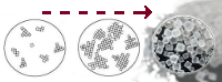
The overlayer is called an epitaxial film or epitaxial layer. The term epitaxy comes from the Greek roots epi (ἐπί), meaning "above", and taxis (τάξις), meaning "an ordered manner". It can be translated as "arranging upon". For most technological applications, it is desired that the deposited material form a crystalline overlayer that has one well-defined orientation with respect to the substrate crystal structure (single-domain epitaxy).
Epitaxial films may be grown from gaseous or liquid precursors. Because the substrate acts as a seed crystal, the deposited film may lock into one or more crystallographic orientations with respect to the substrate crystal. If the overlayer either forms a random orientation with respect to the substrate or does not form an ordered overlayer, it is termed non-epitaxial growth. If an epitaxial film is deposited on a substrate of the same composition, the process is called homoepitaxy; otherwise it is called heteroepitaxy.
Types
Homoepitaxy is a kind of epitaxy performed with only one material, in which a crystalline film is grown on a substrate or film of the same material. This technology is used to grow a film which is more pure than the substrate and to fabricate layers having different doping levels. In academic literature, homoepitaxy is often abbreviated to "homoepi".
Heteroepitaxy is a kind of epitaxy performed with materials that are different from each other. In heteroepitaxy, a crystalline film grows on a crystalline substrate or film of a different material. This technology is often used to grow crystalline films of materials for which crystals cannot otherwise be obtained and to fabricate integrated crystalline layers of different materials. Examples include silicon on sapphire, gallium nitride (GaN) on sapphire, aluminium gallium indium phosphide (AlGaInP) on gallium arsenide (GaAs) or diamond or iridium,[1] and graphene on hexagonal boron nitride.[2]
Heterotopotaxy is a process similar to heteroepitaxy except that thin-film growth is not limited to two-dimensional growth; the substrate is similar only in structure to the thin-film material.
Pendeo-epitaxy is a process in which the heteroepitaxial film is growing vertically and laterally at the same time. In 2D crystal heterostructure, graphenen nanoribbons embedded in hexagonal boron nitride[3][4] are an example for pendeo-epitaxy. Epitaxy is used in silicon-based manufacturing processes for bipolar junction transistors (BJTs) and modern complementary metal–oxide–semiconductors (CMOS), but it is particularly important for compound semiconductors such as gallium arsenide. Manufacturing issues include control of the amount and uniformity of the deposition's resistivity and thickness, the cleanliness and purity of the surface and the chamber atmosphere, the prevention of the typically much more highly doped substrate wafer's diffusion of dopant to the new layers, imperfections of the growth process, and protecting the surfaces during the manufacture and handling.
Applications
Epitaxy is used in nanotechnology and in semiconductor fabrication. Indeed, epitaxy is the only affordable method of high quality crystal growth for many semiconductor materials. In surface science, epitaxy is used to create and study monolayer and multilayer films of adsorbed organic molecules on single crystalline surfaces. Adsorbed molecules form ordered structures on atomically flat terraces of single crystalline surfaces and can directly be observed via scanning tunnelling microscopy.[5] In contrast, surface defects and their geometry have significant influence on the adsorption of organic molecules[6]
Methods
Epitaxial silicon is usually grown using vapor-phase epitaxy (VPE), a modification of chemical vapor deposition. Molecular-beam and liquid-phase epitaxy (MBE and LPE) are also used, mainly for compound semiconductors. Solid-phase epitaxy is used primarily for crystal-damage healing.
Vapor-phase
Silicon is most commonly deposited by doping with silicon tetrachloride and hydrogen at approximately 1200 to 1250 °C:[7]
- SiCl4(g) + 2H2(g) ↔ Si(s) + 4HCl(g)
This reaction is reversible, and the growth rate depends strongly upon the proportion of the two source gases. Growth rates above 2 micrometres per minute produce polycrystalline silicon, and negative growth rates (etching) may occur if too much hydrogen chloride byproduct is present. (In fact, hydrogen chloride may be added intentionally to etch the wafer.) An additional etching reaction competes with the deposition reaction:
- SiCl4(g) + Si(s) ↔ 2SiCl2(g)
Silicon VPE may also use silane, dichlorosilane, and trichlorosilane source gases. For instance, the silane reaction occurs at 650 °C in this way:
- SiH4 → Si + 2H2
This reaction does not inadvertently etch the wafer, and takes place at lower temperatures than deposition from silicon tetrachloride. However, it will form a polycrystalline film unless tightly controlled, and it allows oxidizing species that leak into the reactor to contaminate the epitaxial layer with unwanted compounds such as silicon dioxide.
VPE is sometimes classified by the chemistry of the source gases, such as hydride VPE and metalorganic VPE.
Liquid-phase
Liquid-phase epitaxy (LPE) is a method to grow semiconductor crystal layers from the melt on solid substrates. This happens at temperatures well below the melting point of the deposited semiconductor. The semiconductor is dissolved in the melt of another material. At conditions that are close to the equilibrium between dissolution and deposition, the deposition of the semiconductor crystal on the substrate is relatively fast and uniform. The most used substrate is indium phosphide (InP). Other substrates like glass or ceramic can be applied for special applications. To facilitate nucleation, and to avoid tension in the grown layer the thermal expansion coefficient of substrate and grown layer should be similar.
Centrifugal liquid-phase epitaxy is used commercially to make thin layers of silicon, germanium, and gallium arsenide.[8][9] Centrifugally formed film growth is a process used to form thin layers of materials by using a centrifuge. The process has been used to create silicon for thin-film solar cells[10][11] and far-infrared photodetectors.[12] Temperature and centrifuge spin rate are used to control layer growth.[9] Centrifugal LPE has the capability to create dopant concentration gradients while the solution is held at constant temperature.[13]
Solid-phase
Solid-phase epitaxy (SPE) is a transition between the amorphous and crystalline phases of a material. It is usually done by first depositing a film of amorphous material on a crystalline substrate. The substrate is then heated to crystallize the film. The single crystal substrate serves as a template for crystal growth. The annealing step used to recrystallize or heal silicon layers amorphized during ion implantation is also considered one type of Solid Phase Epitaxy. The Impurity segregation and redistribution at the growing crystal-amorphous layer interface during this process is used to incorporate low-solubility dopants in metals and Silicon.[14]
Molecular-beam epitaxy
In molecular beam epitaxy (MBE), a source material is heated to produce an evaporated beam of particles. These particles travel through a very high vacuum (10−8 Pa; practically free space) to the substrate, where they condense. MBE has lower throughput than other forms of epitaxy. This technique is widely used for growing periodic groups III, IV, and V semiconductor crystals.[15][16] h
Doping
An epitaxial layer can be doped during deposition by adding impurities to the source gas, such as arsine, phosphine, or diborane. The concentration of impurity in the gas phase determines its concentration in the deposited film. As in chemical vapor deposition (CVD), impurities change the deposition rate. Additionally, the high temperatures at which CVD is performed may allow dopants to diffuse into the growing layer from other layers in the wafer ("out-diffusion"). Also, dopants in the source gas, liberated by evaporation or wet etching of the surface, may diffuse into the epitaxial layer ("autodoping"). The dopant profiles of underlying layers change as well, however not as significantly.
Minerals
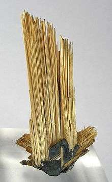
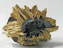
In mineralogy, epitaxy is the overgrowth of one mineral on another in an orderly way, such that certain crystal directions of the two minerals are aligned. This occurs when some planes in the lattices of the overgrowth and the substrate have similar spacings between atoms.[17]
If the crystals of both minerals are well formed so that the directions of the crystallographic axes are clear then the epitaxic relationship can be deduced just by a visual inspection.[17]
Sometimes many separate crystals form the overgrowth on a single substrate, and then if there is epitaxy all the overgrowth crystals will have a similar orientation. The reverse, however, is not necessarily true. If the overgrowth crystals have a similar orientation there is probably an epitaxic relationship, but it is not certain.[17]
Some authors[18] consider that overgrowths of a second generation of the same mineral species should also be considered as epitaxy, and this is common terminology for semiconductor scientists who induce epitaxic growth of a film with a different doping level on a semiconductor substrate of the same material. For naturally produced minerals, however, the International Mineralogical Association (IMA) definition requires that the two minerals be of different species.[19]
Another man-made application of epitaxy is the making of artificial snow using silver iodide, which is possible because hexagonal silver iodide and ice have similar cell dimensions.[18]
Isomorphic minerals
Minerals that have the same structure (isomorphic minerals) may have epitaxic relations. An example is albite NaAlSi
3O
8 on microcline KAlSi
3O
8. Both these minerals are triclinic, with space group 1, and with similar unit cell parameters, a = 8.16 Å, b = 12.87 Å, c = 7.11 Å, α = 93.45°, β = 116.4°, γ = 90.28° for albite and a = 8.5784 Å, b = 12.96 Å, c = 7.2112 Å, α = 90.3°, β = 116.05°, γ = 89° for microcline.
Polymorphic minerals
Minerals that have the same composition but different structures (polymorphic minerals) may also have epitaxic relations. Examples are pyrite and marcasite, both FeS2, and sphalerite and wurtzite, both ZnS.[17]
Rutile on hematite
Some pairs of minerals that are not related structurally or compositionally may also exhibit epitaxy. A common example is rutile TiO2 on hematite Template:Fe.[17][20] Rutile is tetragonal and hematite is trigonal, but there are directions of similar spacing between the atoms in the (100) plane of rutile (perpendicular to the a axis) and the (001) plane of hematite (perpendicular to the c axis). In epitaxy these directions tend to line up with each other, resulting in the axis of the rutile overgrowth being parallel to the c axis of hematite, and the c axis of rutile being parallel to one of the axes of hematite.[17]
Hematite on magnetite
Another example is hematite Fe3+
2O
3 on magnetite Fe2+
Fe3+
2O
4. The magnetite structure is based on close-packed oxygen anions stacked in an ABC-ABC sequence. In this packing the close-packed layers are parallel to (111) (a plane that symmetrically "cuts off" a corner of a cube). The hematite structure is based on close-packed oxygen anions stacked in an AB-AB sequence, which results in a crystal with hexagonal symmetry.[21]
If the cations were small enough to fit into a truly close-packed structure of oxygen anions then the spacing between the nearest neighbour oxygen sites would be the same for both species. The radius of the oxygen ion, however, is only 1.36 Å[22] and the Fe cations are big enough to cause some variations. The Fe radii vary from 0.49 Å to 0.92 Å,[23] depending on the charge (2+ or 3+) and the coordination number (4 or 8). Nevertheless, the O spacings are similar for the two minerals hence hematite can readily grow on the (111) faces of magnetite, with hematite (001) parallel to magnetite (111).[21]
See also
- Atomic layer epitaxy
- Ehrlich-Schwöbel barrier
- Epitaxial wafer
- Exchange bias
- Gallium nitride
- Heterojunction
- Island growth
- Nano-RAM
- Quantum cascade laser
- Selective area epitaxy
- Silicon on sapphire
- Single event upset
- Thin film / Topotaxy
- Vertical-cavity surface-emitting laser
- Wake Shield Facility
- Zhores Alferov
References
- ↑ M. Schreck et al., Appl. Phys. Lett. 78, 192 (2001); doi:10.1063/1.1337648
- ↑ Tang, Shujie; Wang, Haomin; Wang, Huishan (2015). "Silane-catalysed fast growth of large single-crystalline graphene on hexagonal boron nitride". Nature Communications. 6 (6499): 6499. arXiv:1503.02806. Bibcode:2015NatCo...6E6499T. doi:10.1038/ncomms7499. PMC 4382696. PMID 25757864.
- ↑ Chen, Lingxiu; He, Li; Wang, Huishan (2017). "Oriented graphene nanoribbons embedded in hexagonal boron nitride trenches". Nature Communications. 8 (2017): 14703. arXiv:1703.03145. Bibcode:2017NatCo...814703C. doi:10.1038/ncomms14703. PMC 5347129. PMID 28276532.
- ↑ Chen, Lingxiu; Wang, Haomin; Tang, Shujie (2017). "Edge control of graphene domains grown on hexagonal boron nitride". Nanoscale. 9 (32): 1–6. arXiv:1706.01655. doi:10.1039/C7NR02578E. PMID 28580985.
- ↑ Waldmann, T. (2011). "Growth of an oligopyridine adlayer on Ag(100) – A scanning tunnelling microscopy study". Physical Chemistry Chemical Physics. 13 (46): 20724–8. Bibcode:2011PCCP...1320724W. doi:10.1039/C1CP22546D. PMID 21952443.
- ↑ Waldmann, T. (2012). "The role of surface defects in large organic molecule adsorption: substrate configuration effects". Physical Chemistry Chemical Physics. 14 (30): 10726–31. Bibcode:2012PCCP...1410726W. doi:10.1039/C2CP40800G. PMID 22751288.
- ↑ Morgan, D. V.; Board, K. (1991). An Introduction To Semiconductor Microtechnology (2nd ed.). Chichester, West Sussex, England: John Wiley & Sons. p. 23. ISBN 978-0471924784.
- ↑ Capper, Peter; Mauk, Michael (2007). Liquid Phase Epitaxy of Electronic, Optical and Optoelectronic Materials. John Wiley & Sons. pp. 134–135. ISBN 9780470319499. Retrieved 3 October 2017.
- 1 2 Farrow, R. F. C.; Parkin, S. S. P.; Dobson, P. J.; Neave, J. H.; Arrott, A. S. (2013). Thin Film Growth Techniques for Low-Dimensional Structures. Springer Science & Business Media. pp. 174–176. ISBN 9781468491456. Retrieved 3 October 2017.
- ↑ Christensen, Arnfinn. "Speedy production of silicon for solar cells". sciencenordic.com. ScienceNordic. Retrieved 3 October 2017.
- ↑ Luque, A.; Sala, G.; Palz, Willeke; Santos, G. dos; Helm, P. (2012). Tenth E.C. Photovoltaic Solar Energy Conference: Proceedings of the International Conference, held at Lisbon, Portugal, 8–12 April 1991. Springer. p. 694. ISBN 9789401136228. Retrieved 3 October 2017.
- ↑ Katterloher, Reinhard O.; Jakob, Gerd; Konuma, Mitsuharu; Krabbe, Alfred; Haegel, Nancy M.; Samperi, S. A.; Beeman, Jeffrey W.; Haller, Eugene E. (8 February 2002). "Liquid phase epitaxy centrifuge for growth of ultrapure gallium arsenide for far-infrared photoconductors". Infrared Spaceborne Remote Sensing Ix. 4486: 200–209. Bibcode:2002SPIE.4486..200K. doi:10.1117/12.455132.
- ↑ Pauleau, Y. (2012). Chemical Physics of Thin Film Deposition Processes for Micro- and Nano-Technologies. Springer Science & Business Media. p. 45. ISBN 9789401003537. Retrieved 3 October 2017.
- ↑ Custer, J.S.; Polman, A.; Pinxteren, H. M. (15 March 1994). "Erbium in crystal silicon: Segregation and trapping during solid phase epitaxy of amorphous silicon". Journal of Applied Physics. 75 (6): 2809. Bibcode:1994JAP....75.2809C. doi:10.1063/1.356173.
- ↑ A. Y. Cho, "Growth of III\–V semiconductors by molecular beam epitaxy and their properties," Thin Solid Films, vol. 100, pp. 291–317, 1983.
- ↑ Cheng, K. Y. (November 1997). "Molecular beam epitaxy technology of III-V compound semiconductors for optoelectronic applications". Proceedings of the IEEE. 85 (11): 1694–1714. doi:10.1109/5.649646. ISSN 0018-9219.
- 1 2 3 4 5 6 Rakovan, John (2006) Rocks & Minerals 81:317 to 320
- 1 2 White and Richards (2010) Rocks & Minerals 85:173 to 176
- ↑ Acta Crystallographica Section A Crystal Physics, Diffraction, Theoretical and General Crystallography Volume 33, Part 4 (July 1977)
- ↑ "FMF - Friends of Minerals Forum, discussion and message board :: Index". www.mineral-forum.com/message-board/.
- 1 2 Nesse, William (2000). Introduction to Mineralogy. Oxford University Press. Page 79
- ↑ Klein, Cornelis; Hurlbut, Cornelius Searle; Dana, James Dwight (1993). Manual of mineralogy. Wiley. ISBN 978-0-471-57452-1.
- ↑ "Imperial College Database".
Bibliography
- Jaeger, Richard C. (2002). "Film Deposition". Introduction to Microelectronic Fabrication (2nd ed.). Upper Saddle River: Prentice Hall. ISBN 978-0-201-44494-0.
External links
| Wikimedia Commons has media related to |
- epitaxy.net: a central forum for the epitaxy-communities
- Deposition processes
- CrystalXE.com: a specialized software in epitaxy