Carbon nanobud
In nanotechnology, a carbon nanobud is a material that combines carbon nanotubes and spheroidal fullerenes, both allotropes of carbon, in the same structure, forming "buds" attached to the tubes. Carbon nanobuds were discovered and synthesized in 2006.
In this material, fullerenes are covalently bonded to the outer sidewalls of the underlying nanotube. Consequently, nanobuds exhibit properties of both carbon nanotubes and fullerenes. For instance, the mechanical properties and the electrical conductivity of the nanobuds are similar to those of corresponding carbon nanotubes. However, because of the higher reactivity of the attached fullerene molecules, the hybrid material can be further functionalized through known fullerene chemistry. Additionally, the attached fullerene molecules can be used as molecular anchors to prevent slipping of the nanotubes in various composite materials, thus modifying the composite’s mechanical properties.[2][3]
Owing to the large number of highly curved fullerene surfaces acting as electron emission sites on conductive carbon nanotubes, nanobuds possess advantageous field electron emission characteristics. Randomly oriented nanobuds have already been demonstrated to have an extremely low work function for field electron emission. Reported test measurements show (macroscopic) field thresholds of about 0.65 V/μm, (non-functionalized single-walled carbon nanotubes have a macroscopic field threshold for field electron emission ~2 V/μm) and a much higher current density as compared with that of the corresponding pure single-walled carbon nanotubes.[2] The electron transport properties of certain nanobud classes have been treated theoretically.[4] The study shows that electrons indeed pass to the neck and bud region of the nanobud system.
Canatu Oy, a Finnish company, claims the intellectual property rights for nanobud material, its synthesis processes, and several applications.[5]
Properties
Carbon nanobuds (CNBs) have some properties of nanotubes such as one-dimensional electrical conductivity, flexibility and adaptability to manufacture while also having some chemical properties of fullerenes. Examples of these properties include engaging in cycloaddition reactions and can easily form the chemical bonds capable of attaching to other molecules with complex structures. CNBs have a much higher chemical activity than single walled carbon nanotubes (SWCNTs).[6]
Electrical Properties
This new structure has been shown to have electronic properties that differ from those of fullerenes and carbon nanotubes (CNTs). CNBs exhibit lower field thresholds and higher current densities and electric field emission than SWCNTs.[7] The chemical bonds between the nanotube's wall and the fullerenes on the surface can lead to charge transfer between the surfaces.[7] The presence of fullerenes in CNBs lead to smaller bundle formation and larger chemical reactivity.[7] CNBs can engage in cycloaddiiton reactions and easily form the chemical bonds capable of attaching molecules with complex structures. this can be explained by a greater availability of CNB surface to the reactants the presence of π-conjugated structures, and having 5-atom rings with excess pirimidization energy.[8] Formation energy indicated that preparation of CNBs is endothermic, meaning that its not favorable to create.[9]
All CNBs are conducting, regardless of whether the single walled CNT is a metallic or semiconducting base. The band gap of carbon nanobuds is not constant, it can change through the size of the fullerene group.[6] The attachment of C60 added to the armchair orientation of the SWCNT opens up the band gap. On the other hand, adding it to a semiconducting SWCNT could introduce impurity states to the band gap, which would reduce the band gap. The band gap of CNBs can also be modified by changing the density of the carbons of the C60 attached to the sidewall of the SWCNT.[10]
Magnetic Properties
Geometrical factors are integral to study the magnetic properties of nanobuds. There are two structures of CNBs that are ferromagnetic in their ground state, and two that are nonmagnetic.[11] The attached C60 molecule on the surface of the CNTs gives more space between the nanotubes and adhesion between the single walled CNTS can be weakened to prevent the formation of tight bundles of CNTs.[6] Carbon nanobuds can be used as molecular support to prevent slipping of the matrix in composite materials and to increase the mechanical strength of them.[7]
Structural Properties
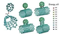
The stability of CNBs is dependent on the type of carbon-carbon bond that is dissociated in the cycloaddition reaction. It has been shown that carbon atoms of the SWCNT near the fullerene C60 molecule were pulled outward from the original wall surface due to the covalent bonding with cycloaddition reaction between the fullerene and nanotube; in addition, their bonding was transformed from sp2 to sp3 hybridization.[7] An analysis using Raman scattering spectroscopy shows that the CNB sample had stronger chemical modification compared to CNTs. This indicates that there is a carbon sp3 hybridization that occurs after the chemical addition creation of CNBs.[6]
Synthesis
The single wall carbon nanotubes, SWCNTs, are capable of being covered with covalently bonded fullerenes (a specific type of spheroidal carbon). This was able to occur when water vapor or carbon dioxide concentrations were instituted into the reactor. This occurrence produces a material that looks similar to buds that are on a tree branch. Therefore, this is the reasoning behind the term, nanobud, being chosen for the material.[8]
The vapor concentrations for the water and the density of the fullerenes were looked into with a lot more detail. At 45 ppm and higher, the nanobuds began to be formed in abundance. However, when the concentration for the water that was added was about 365 ppm, something different happened. Rather than being a significant amount of nanobuds, it contained a large amount of inactive catalyst particles.[8]
Characterization
There are multiple methods that were used in order to discover the fullerenes on the single wall carbon nanotube surfaces, each giving its own contribution to what is currently known about nanobuds. A few of these methods are ultraviolet-visible spectroscopy (UV-Vis), transmission electron microscopy (TEM), and scanning tunneling microscopy (STM).
To look even further into the functionality of CNBs and how the single wall carbon nanotubes interact with the fullerenes to produce the nanobuds, calculations were done. The calculations that were done came from the atomistic density functional theory (quantum mechanical modelling method) and gave quite a bit of information about the bonding that is taking place. They told the scientists that there seem to be two possibilities for the interaction. One of the possibilities is that the fullerenes can be covalently bonded to the single wall carbon nanotubes directly. The other possibility is that the fullerenes are forming hybrid structures.[8]
Regardless of how they are bonding to the single wall nanotubes, studies have shown that the fullerenes are stationary and do not seem to want to move from the interaction with the nanotubes, concluding that the bond they have is very strong. This study was done using transmission electron microscopy.
Another study was done to see how washing the nanobuds in different solvents, such as toluene, decaline, and hexane, would affect the fullerenes and their interaction with the nanotubes. Of the solvents that were tested, none of them resulted in fullerenes being dissolved in the solvent. This continues to defend the discovery that the bond between the two is significantly strong. In one more additional study that was done, it was discovered that each of the nanobud samples contained oxygen.[2]
Applications
The research, development, and manufacture of flexible and transparent electronics relies on novel materials, or materials which are mechanically flexible, lightweight and relatively low cost. These materials must also be conductive and optically transparent. Due to their close relation to the carbon nanotube family, carbon NanoBuds offer all of those traits, as well as more due to their inclusion of fullerene.
Esko Kauppinen, a professor and researcher at the Helsinki University of Technology and the technology development organization VTT Biotechnology, and his team found that carbon NanoBuds have properties that are often associated with cold electron field emitters.[12] Such materials emit electrons at room temperature under a high applied electric field, a property that is very important with regard to technologies such as flat-panel displays and electron microscopes.[12] Carbon NanoBuds can be much more effective than flat surfaces with respect to how efficiently they can emit electrons. This is due to the many curved surfaces of both the fullerene and the carbon nanotube that make up the carbon NanoBud.
As a result of the curvature of the fullerenes and the nanotubes, almost any surface could potentially be transformed into a surface with touch sensing ability. Canatu, a company which specializes in electronic carbon NanoBud products, claims that the films that result from the synthesis of the NanoBuds are very rugged and flexible. They also claim that the NanoBuds allow for easy application to flexible and curved surfaces. NanoBuds are able to maintain their electronic capabilities while being bent up to 200 percent. This property is a result of the rounded surfaces, which allow the NanoBuds to slide past each other without damaging the electronic structure of the material.[13] Typically, touch screen surfaces are made by placing a sheet of indium tin oxide, also a transparent film, over a display screen. However, indium tin oxide sheets are very brittle like glass and can only be applied to relatively flat surfaces in order to maintain the integrity of the structure.[13]
As a result of their close lineage with carbon nanotubes, NanoBuds have a tunable electrical conductivity.[14] Since the electrical properties of the NanoBuds can be individually tuned (provided that single wall nanotubes with distinct regions of different electrical properties are a part of the NanoBud), according to Esko Kauppinen and his team, it is entirely possible that NanoBuds may at some point be used in applications such as memory storage devices and quantum dots. The Kauppinen team argues that the conductivity of the crystalline carbon structure allow for this application. In fact, the small size of carbon nanotubes and carbon NanoBuds, in theory, allow for a very high density of energy storage.[15] The most common memory technology that is associated with carbon NanoBuds is Nano random-access memory (NRAM), or Nano-RAM. This technology is a type of nonvolatile random access memory, but it is based on the position of carbon nanotubes, or in this case, carbon NanoBuds on a chip like substrate.[15] Its developing company Nantero give it its common name, NRAM. When compared to other forms of nonvolatile random access memory, NanoRAM has several advantages, but one really stands out. NRAM is believed to be within a variety of new memory systems, a variety which many people believe to be universal. Nantero claims that Nano-RAM (NRAM) could eventually replace almost all memory systems from flash to DRAM to SRAM.
See also
References
| Wikimedia Commons has media related to Carbon nanobuds. |
- 1 2 3 Gorantla, Sandeep; Börrnert, Felix; Bachmatiuk, Alicja; Dimitrakopoulou, Maria; Schönfelder, Ronny; Schäffel, Franziska; Thomas, Jürgen; Gemming, Thomas; Borowiak-Palen, Ewa; Warner, Jamie H.; Yakobson, Boris I.; Eckert, Jürgen; Büchner, Bernd; Rümmeli, Mark H. (2010). "In situ observations of fullerene fusion and ejection in carbon nanotubes". Nanoscale. 2 (10): 2077. Bibcode:2010Nanos...2.2077G. doi:10.1039/C0NR00426J. PMID 20714658.
- 1 2 3 Nasibulin, Albert G.; et al. (2007). "A novel hybrid carbon material" (PDF). Nature Nanotechnology. 2 (3): 156&ndash, 161. doi:10.1038/nnano.2007.37. PMID 18654245.
- ↑ Nasibulin, Albert G.; et al. (2007). "Investigations of NanoBud formation" (PDF). Chemical Physics Letters. 446: 109–114. doi:10.1016/j.cplett.2007.08.050.
- ↑ Fürst, Joachim A.; et al. (2009). "Electronic transport properties of fullerene functionalized carbon nanotubes: Ab initio and tight-binding calculations". Physical Review B. 80 (3): 115117. doi:10.1103/PhysRevB.80.035427.
- ↑ "European Patent Office: search CANATU". Retrieved 2010-06-03.
- 1 2 3 4 Albert G. Nasibulin Ilya V. Anoshkin, Prasantha R. Mudimela, Janne Raula, Vladimir Ermolov, Esko I. Kauppinen, "Selective Chemical Functionalization of Carbon Nanobuds," Carbon 50, no. 11 (2012).
- 1 2 3 4 5 M. Ghorbanzadeh Ahangari, M.D. Ganji, F. Montazar. "Mechanical and Electronic Properties of Carbon Nanobuds: First-Principles Study." Solid State Communication 203 (2015): 58-62.
- 1 2 3 4 Anisimov, Anton. "Aerosol Synthesis of Carbon Nanotubes and Nanobuds.". (2010).
- ↑ Seif, A., E. Zahedi, and T. S. Ahmadi. "A Dft Study of Carbon Nanobuds." The European Physical Journal B 82, no. 2 (July 01 2011): 147-52.
- ↑ Xiaojun Wu and Xiao Cheng Zeng, "First-Principles Study of a Carbon Nanobud," ACS Nano 2, no. 7 (2008)
- ↑ Min Wang and Chang Ming Li, "Magnetic Properties of All-Carbon Graphene-Fullerene Nanobuds," Physical Chemistry Chemical Physics 13, no. 13 (2011).
- 1 2 Clarke, Peter (21 Nov 2014). "Carbon 'nanobuds' enable transparent touch sensors on 3D surfaces". Eenewsanalog.com.
- 1 2 Bullis, Kevin (11 Dec 2014). "Startup Tests Nanobud Touch Sensors". MIT Technology Review.
- ↑ Mgrdichian, Laura (30 Mar 2007). "New Nanomaterial, NanoBuds, Combines Fullerenes and ..."
- 1 2 "Electronics". Nanotechmag.com.
| sp3 forms | |
|---|---|
| sp2 forms | |
| sp forms | |
| mixed sp3/sp2 forms | |
| other forms | |
| hypothetical forms | |
| related | |
| |