Photonic crystal
A photonic crystal is a periodic optical nanostructure that affects the motion of photons in much the same way that ionic lattices affect electrons in solids. Photonic crystals occur in nature in the form of structural coloration and animal reflectors, and, in different forms, promise to be useful in a range of applications.
In 1887 the English physicist Lord Rayleigh experimented with periodic multi-layer dielectric stacks, showing they had a photonic band-gap in one dimension. Research interest grew with work in 1987 by Eli Yablonovitch and Sajeev John on periodic optical structures with more than one dimension—now called photonic crystals.
Photonic crystals can be fabricated for one, two, or three dimensions. One-dimensional photonic crystals can be made of layers deposited or stuck together. Two-dimensional ones can be made by photolithography, or by drilling holes in a suitable substrate. Fabrication methods for three-dimensional ones include drilling under different angles, stacking multiple 2-D layers on top of each other, direct laser writing, or, for example, instigating self-assembly of spheres in a matrix and dissolving the spheres.
Photonic crystals can, in principle, find uses wherever light must be manipulated. Existing applications include thin-film optics with coatings for lenses. Two-dimensional photonic-crystal fibers are used in nonlinear devices and to guide exotic wavelengths. Three-dimensional crystals may one day be used in optical computers. Three-dimensional photonic crystals could lead to more efficient photovoltaic cells as a source of power for electronics, thus cutting down the need for an electrical input for power.[3]
Introduction
Photonic crystals are composed of periodic dielectric, metallo-dielectric—or even superconductor microstructures or nanostructures that affect electromagnetic wave propagation in the same way that the periodic potential in a semiconductor crystal affects electron motion by defining allowed and forbidden electronic energy bands. Photonic crystals contain regularly repeating regions of high and low dielectric constant. Photons (behaving as waves) either propagate through this structure or not, depending on their wavelength. Wavelengths that propagate are called modes, and groups of allowed modes form bands. Disallowed bands of wavelengths are called photonic band gaps. This gives rise to distinct optical phenomena, such as inhibition of spontaneous emission,[4] high-reflecting omni-directional mirrors, and low-loss-waveguiding. Intuitively, the bandgap of photonic crystals can be understood to arise from the destructive interference of multiple reflections of light propagating in the crystal at the interfaces of the high- and low- dielectric constant regions, akin to the bandgaps of electrons in solids.
The periodicity of the photonic crystal structure must be around half the wavelength of the electromagnetic waves to be diffracted. This is ~350 nm (blue) to ~650 nm (red) for photonic crystals that operate in the visible part of the spectrum—or even less, depending on average index of refraction. The repeating regions of high and low dielectric constant must, therefore, be fabricated at this scale, which is difficult.
History
Photonic crystals have been studied in one form or another since 1887, but no one used the term photonic crystal until over 100 years later—after Eli Yablonovitch and Sajeev John published two milestone papers on photonic crystals in 1987.[4][5] The early history is well documented in the form of a story when it was identified as one of the landmark developments in physics by the American Physical Society[6].
Before 1987, one-dimensional photonic crystals in the form of periodic multi-layer dielectric stacks (such as the Bragg mirror) were studied extensively. Lord Rayleigh started their study in 1887,[7] by showing that such systems have a one-dimensional photonic band-gap, a spectral range of large reflectivity, known as a stop-band. Today, such structures are used in a diverse range of applications—from reflective coatings to enhancing LED efficiency to highly reflective mirrors in certain laser cavities (see, for example, VCSEL). A detailed theoretical study of one-dimensional optical structures was performed by Vladimir P. Bykov,[8] who was the first to investigate the effect of a photonic band-gap on the spontaneous emission from atoms and molecules embedded within the photonic structure. Bykov also speculated as to what could happen if two- or three-dimensional periodic optical structures were used.[9] The concept of three-dimensional photonic crystals was then discussed by Ohtaka in 1979,[10] who also developed a formalism for the calculation of the photonic band structure. However, these ideas did not take off until after the publication of two milestone papers in 1987 by Yablonovitch and John. Both these papers concerned high-dimensional periodic optical structures, i.e., photonic crystals. Yablonovitch's main goal was to engineer photonic density of states to control the spontaneous emission of materials embedded in the photonic crystal. John's idea was to use photonic crystals to affect localisation and control of light.
After 1987, the number of research papers concerning photonic crystals began to grow exponentially. However, due to the difficulty of fabricating these structures at optical scales (see Fabrication challenges), early studies were either theoretical or in the microwave regime, where photonic crystals can be built on the more accessible centimetre scale. (This fact is due to a property of the electromagnetic fields known as scale invariance. In essence, electromagnetic fields, as the solutions to Maxwell's equations, have no natural length scale—so solutions for centimetre scale structure at microwave frequencies are the same as for nanometre scale structures at optical frequencies.)
By 1991, Yablonovitch had demonstrated the first three-dimensional photonic band-gap in the microwave regime.[11] The structure that Yablonvitch was able to produce involved drilling an array of holes in a transparent material, where the holes of each layer form an inverse diamond structure – today it is known as Yablonovite.
In 1996, Thomas Krauss demonstrated a two-dimensional photonic crystal at optical wavelengths.[12] This opened the way to fabricate photonic crystals in semiconductor materials by borrowing methods from the semiconductor industry.
Today, such techniques use photonic crystal slabs, which are two dimensional photonic crystals "etched" into slabs of semiconductor. Total internal reflection confines light to the slab, and allows photonic crystal effects, such as engineering photonic dispersion in the slab. Researchers around the world are looking for ways to use photonic crystal slabs in integrated computer chips, to improve optical processing of communications—both on-chip and between chips.
Such techniques have yet to mature into commercial applications, but two-dimensional photonic crystals are commercially used in photonic crystal fibres[13] (otherwise known as holey fibres, because of the air holes that run through them). Photonic crystal fibres were first developed by Philip Russell in 1998, and can be designed to possess enhanced properties over (normal) optical fibres.
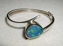
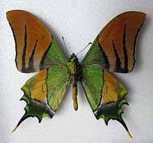
Study has proceeded more slowly in three-dimensional than in two-dimensional photonic crystals. This is because of more difficult fabrication.[13] Three-dimensional photonic crystal fabrication had no inheritable semiconductor industry techniques to draw on. Attempts have been made, however, to adapt some of the same techniques, and quite advanced examples have been demonstrated,[14] for example in the construction of "woodpile" structures constructed on a planar layer-by-layer basis. Another strand of research has tried to construct three-dimensional photonic structures from self-assembly—essentially letting a mixture of dielectric nano-spheres settle from solution into three-dimensionally periodic structures that have photonic band-gaps. Vasily Astratov's group from the Ioffe Institute realized in 1995 that natural and synthetic opals are photonic crystals with an incomplete bandgap.[15] The first demonstration of an "inverse opal" structure with a complete photonic bandgap came in 2000, from researchers at the University of Toronto, Canada.[16] The ever-expanding field of biomimetics—the study of natural structures to better understand and use them in design—is also helping researchers in photonic crystals.[17][18] For example, in 2006 a naturally occurring photonic crystal was discovered in the scales of a Brazilian beetle.[19] Analogously, in 2012 a diamond crystal structure was found in a weevil[20][21] and a gyroid-type architecture in a butterfly.[22]
Construction strategies
The fabrication method depends on the number of dimensions that the photonic bandgap must exist in.
- Examples of possible photonic crystal structures in 1, 2 and 3 dimensions
 Comparison of 1D, 2D and 3D photonic crystal structures (from left to right, respectively).
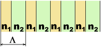 Schematic of a 1D photonic crystal structure, made of alternating layers of a high-dielectric constant material and a low-dielectric constant material. These layers are typically quarter wavelength in thickness.
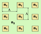 2D photonic crystal structure in a square array.
 Schematic of a 2D photonic crystal made of circular holes.
 A woodpile structured 3D photonic crystal. These structures have a three-dimensional bandgap for all polarizations
One-dimensional photonic crystals
In a one-dimensional photonic crystal, layers of different dielectric constant may be deposited or adhered together to form a band gap in a single direction. A Bragg grating is an example of this type of photonic crystal. One-dimensional photonic crystals can be either isotropic or anisotropic, with the latter having potential use as an optical switch.[23]
One-dimensional photonic crystal can form as an infinite number of parallel alternating layers filled with a metamaterial and vacuum.[24] This produces identical PBG structures for TE and TM modes.
Recently, researchers fabricated a graphene-based Bragg grating (one-dimensional photonic crystal) and demonstrated that it supports excitation of surface electromagnetic waves in the periodic structure by using 633 nm He-Ne laser as the light source.[25] Besides, a novel type of one-dimensional graphene-dielectric photonic crystal has also been proposed. This structure can act as a far-IR filter and can support low-loss surface plasmons for waveguide and sensing applications.[26]
Two-dimensional photonic crystals
In two dimensions, holes may be drilled in a substrate that is transparent to the wavelength of radiation that the bandgap is designed to block. Triangular and square lattices of holes have been successfully employed.
The Holey fiber or photonic crystal fiber can be made by taking cylindrical rods of glass in hexagonal lattice, and then heating and stretching them, the triangle-like airgaps between the glass rods become the holes that confine the modes.
Three-dimensional photonic crystals
There are several structure types that have been constructed:[27]
- Spheres in a diamond lattice
- Yablonovite
- The woodpile structure – "rods" are repeatedly etched with beam lithography, filled in, and covered with a layer of new material. As the process repeats, the channels etched in each layer are perpendicular to the layer below, and parallel to and out of phase with the channels two layers below. The process repeats until the structure is of the desired height. The fill-in material is then dissolved using an agent that dissolves the fill-in material but not the deposition material. It is generally hard to introduce defects into this structure.
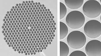
- Inverse opals or Inverse Colloidal Crystals-Spheres (such as polystyrene or silicon dioxide) can be allowed to deposit into a cubic close packed lattice suspended in a solvent. Then a hardener is introduced that makes a transparent solid out of the volume occupied by the solvent. The spheres are then dissolved with an acid such as Hydrochloric acid. The colloids can be either spherical[16] or nonspherical.[28][29][30]
- A stack of two-dimensional crystals – This is a more general class of photonic crystals than Yablonovite, but the original implementation of Yablonovite was created using this method.
- "The photonic crystal beam splitter that we made is a fundamental optical component used to control polarized light," explains Dr Mark Turner from Swinburne University. "Specifically what makes our device unique is its ability to directly work with circular polarization at a microscopic scale."
- Circular polarization uses 3D laser nanotechnology to exploit circular polarization to build a microscopic prism that contains in excess of 750,000 polymer nanorods. Light focused on this beam splitter penetrates or is reflected, depending on polarization.[31][32]

Fabrication challenges
Higher-dimensional photonic crystal fabrication faces two major challenges:
- Making them with enough precision to prevent scattering losses blurring the crystal properties
- Designing processes that can robustly mass-produce the crystals
One promising fabrication method for two-dimensionally periodic photonic crystals is a photonic-crystal fiber, such as a holey fiber. Using fiber draw techniques developed for communications fiber it meets these two requirements, and photonic crystal fibres are commercially available. Another promising method for developing two-dimensional photonic crystals is the so-called photonic crystal slab. These structures consist of a slab of material—such as silicon—that can be patterned using techniques from the semiconductor industry. Such chips offer the potential to combine photonic processing with electronic processing on a single chip.
For three dimensional photonic crystals, various techniques have been used—including photolithography and etching techniques similar to those used for integrated circuits.[14] Some of these techniques are already commercially available. To avoid the complex machinery of nanotechnological methods, some alternate approaches involve growing photonic crystals from colloidal crystals as self-assembled structures.
Mass-scale 3D photonic crystal films and fibres can now be produced using a shear-assembly technique that stacks 200–300 nm colloidal polymer spheres into perfect films of fcc lattice. Because the particles have a softer transparent rubber coating, the films can be stretched and molded, tuning the photonic bandgaps and producing striking structural color effects.
Computing photonic band structure
The photonic band gap (PBG) is essentially the gap between the air-line and the dielectric-line in the dispersion relation of the PBG system. To design photonic crystal systems, it is essential to engineer the location and size of the bandgap by computational modeling using any of the following methods:
- Plane wave expansion method
- Finite element method
- Finite difference time domain method
- Order-n spectral method[34][35]
- KKR method
- Bloch wave – MoM method
- Construction of the Band Diagram[36]
Essentially, these methods solve for the frequencies (normal modes) of the photonic crystal for each value of the propagation direction given by the wave vector, or vice versa. The various lines in the band structure, correspond to the different cases of n, the band index. For an introduction to photonic band structure, see Joannopoulos.[37]

The plane wave expansion method can be used to calculate the band structure using an eigen formulation of the Maxwell's equations, and thus solving for the eigen frequencies for each of the propagation directions, of the wave vectors. It directly solves for the dispersion diagram. Electric field strength values can also be calculated over the spatial domain of the problem using the eigen vectors of the same problem. For the picture shown to the right, corresponds to the band-structure of a 1D distributed Bragg reflector (DBR) with air-core interleaved with a dielectric material of relative permittivity 12.25, and a lattice period to air-core thickness ratio (d/a) of 0.8, is solved using 101 planewaves over the first irreducible Brillouin zone.
To speed calculation of the frequency band structure, the Reduced Bloch Mode Expansion (RBME) method can be used.[38] The RBME method applies "on top" of any of the primary expansion methods mentioned above. For large unit cell models, the RBME method can reduce time for computing the band structure by up to two orders of magnitude.
Applications
Photonic crystals are attractive optical materials for controlling and manipulating light flow. One dimensional photonic crystals are already in widespread use, in the form of thin-film optics, with applications from low and high reflection coatings on lenses and mirrors to colour changing paints and inks. Higher-dimensional photonic crystals are of great interest for both fundamental and applied research, and the two dimensional ones are beginning to find commercial applications.
The first commercial products involving two-dimensionally periodic photonic crystals are already available in the form of photonic-crystal fibers, which use a microscale structure to confine light with radically different characteristics compared to conventional optical fiber for applications in nonlinear devices and guiding exotic wavelengths. The three-dimensional counterparts are still far from commercialization but may offer additional features such as optical nonlinearity required for the operation of optical transistors used in optical computers, when some technological aspects such as manufacturability and principal difficulties such as disorder are under control.
See also
References
- ↑ Proietti Zaccaria, Remo (2016). "Butterfly wing color: A photonic crystal demonstration". Optics and Lasers in Engineering. 76: 70–3. Bibcode:2016OptLE..76...70P. doi:10.1016/j.optlaseng.2015.04.008.
- ↑ Biró, L.P; Kertész, K; Vértesy, Z; Márk, G.I; Bálint, Zs; Lousse, V; Vigneron, J.-P (2007). "Living photonic crystals: Butterfly scales — Nanostructure and optical properties". Materials Science and Engineering: C. 27 (5–8): 941–6. doi:10.1016/j.msec.2006.09.043.
- ↑ Hwang, Dae-Kue; Lee, Byunghong; Kim, Dae-Hwan (2013). "Efficiency enhancement in solid dye-sensitized solar cell by three-dimensional photonic crystal". RSC Advances. 3 (9): 3017–23. doi:10.1039/C2RA22746K.
- 1 2 Yablonovitch, Eli (1987). "Inhibited Spontaneous Emission in Solid-State Physics and Electronics". Physical Review Letters. 58 (20): 2059–62. Bibcode:1987PhRvL..58.2059Y. doi:10.1103/PhysRevLett.58.2059. PMID 10034639.
- ↑ John, Sajeev (1987). "Strong localization of photons in certain disordered dielectric superlattices". Physical Review Letters. 58 (23): 2486–9. Bibcode:1987PhRvL..58.2486J. doi:10.1103/PhysRevLett.58.2486. PMID 10034761.
- ↑ Lindley, David (2013-08-23). "Focus: Landmarks—The Birth of Photonic Crystals". Physics. 6.
- ↑ Rayleigh, Lord (2009). "XXVI. On the remarkable phenomenon of crystalline reflexion described by Prof. Stokes". The London, Edinburgh, and Dublin Philosophical Magazine and Journal of Science. 26 (160): 256–65. doi:10.1080/14786448808628259.
- ↑ Bykov, V. P (1972). "Spontaneous Emission in a Periodic Structure". Soviet Journal of Experimental and Theoretical Physics. 35: 269. Bibcode:1972JETP...35..269B.
- ↑ Bykov, Vladimir P (1975). "Spontaneous emission from a medium with a band spectrum". Soviet Journal of Quantum Electronics. 4 (7): 861–871. Bibcode:1975QuEle...4..861B. doi:10.1070/QE1975v004n07ABEH009654.
- ↑ Ohtaka, K (1979). "Energy band of photons and low-energy photon diffraction". Physical Review B. 19 (10): 5057–67. Bibcode:1979PhRvB..19.5057O. doi:10.1103/PhysRevB.19.5057.
- ↑ Yablonovitch, E; Gmitter, T; Leung, K (1991). "Photonic band structure: The face-centered-cubic case employing nonspherical atoms". Physical Review Letters. 67 (17): 2295–2298. Bibcode:1991PhRvL..67.2295Y. doi:10.1103/PhysRevLett.67.2295. PMID 10044390.
- ↑ , Bibcode:1996Natur.383..699K, doi:10.1038/383699a0 Missing or empty
|title=(help) - 1 2 Jennifer Ouellette (2002), "Seeing the Future in Photonic Crystals" (PDF), The Industrial Physicist, 7 (6): 14–17, archived from the original (PDF) on August 12, 2011
- 1 2 Review: S. Johnson (MIT) Lecture 3: Fabrication technologies for 3d photonic crystals, a survey
- ↑ Astratov, V. N; Bogomolov, V. N; Kaplyanskii, A. A; Prokofiev, A. V; Samoilovich, L. A; Samoilovich, S. M; Vlasov, Yu. A (1995). "Optical spectroscopy of opal matrices with CdS embedded in its pores: Quantum confinement and photonic band gap effects". Il Nuovo Cimento D. 17 (11–12): 1349–54. Bibcode:1995NCimD..17.1349A. doi:10.1007/bf02457208.
- 1 2 Blanco, Alvaro; Chomski, Emmanuel; Grabtchak, Serguei; Ibisate, Marta; John, Sajeev; Leonard, Stephen W; Lopez, Cefe; Meseguer, Francisco; Miguez, Hernan; Mondia, Jessica P; Ozin, Geoffrey A; Toader, Ovidiu; Van Driel, Henry M (2000). "Large-scale synthesis of a silicon photonic crystal with a complete three-dimensional bandgap near 1.5 micrometres". Nature. 405 (6785): 437–40. Bibcode:2000Natur.405..437B. doi:10.1038/35013024. PMID 10839534.
- ↑ Kolle, Mathias (2011), "Photonic Structures Inspired by Nature", Photonic Structures Inspired by Nature: (1st ed.), Bibcode:2011psin.book.....K, doi:10.1007/978-3-642-15169-9, ISBN 978-3-642-15168-2
- ↑ McPhedran, Ross C; Parker, Andrew R (2015). "Biomimetics: Lessons on optics from nature's school". Physics Today. 68 (6): 32. Bibcode:2015PhT....68f..32M. doi:10.1063/PT.3.2816.
- ↑ Galusha, Jeremy W; Richey, Lauren R; Gardner, John S; Cha, Jennifer N; Bartl, Michael H (2008). "Discovery of a diamond-based photonic crystal structure in beetle scales". Physical Review E. 77 (5): 050904. Bibcode:2008PhRvE..77e0904G. doi:10.1103/PhysRevE.77.050904. PMID 18643018.
- ↑ Wilts, B. D; Michielsen, K; Kuipers, J; De Raedt, H; Stavenga, D. G (2012). "Brilliant camouflage: Photonic crystals in the diamond weevil, Entimus imperialis". Proceedings of the Royal Society B: Biological Sciences. 279 (1738): 2524–30. doi:10.1098/rspb.2011.2651. PMC 3350696. PMID 22378806.
- ↑ Wilts, B. D; Michielsen, K; De Raedt, H; Stavenga, D. G (2011). "Hemispherical Brillouin zone imaging of a diamond-type biological photonic crystal". Journal of the Royal Society Interface. 9 (72): 1609–14. doi:10.1098/rsif.2011.0730. PMC 3367810. PMID 22188768.
- ↑ Wilts, B. D; Michielsen, K; De Raedt, H; Stavenga, D. G (2011). "Iridescence and spectral filtering of the gyroid-type photonic crystals in Parides sesostris wing scales". Interface Focus. 2 (5): 681–7. doi:10.1098/rsfs.2011.0082. PMC 3438581. PMID 24098853.
- ↑ Cao, Y; Schenk, J. O; Fiddy, M. A (2008). "Third Order Nonlinear Effect Near a Degenerate Band Edge". Optics and Photonics Letters. 1 (1): 1–7. doi:10.1142/S1793528808000033.
- ↑ Pravdin, K. V.; Popov, I. Yu. (2014). "Photonic crystal with negative index material layers" (PDF). Nanosystems: Physics, Chemistry, Mathematics. 5 (5): 626–643.
- ↑ Sreekanth, Kandammathe Valiyaveedu; Zeng, Shuwen; Shang, Jingzhi; Yong, Ken-Tye; Yu, Ting (2012). "Excitation of surface electromagnetic waves in a graphene-based Bragg grating". Scientific Reports. 2: 737. Bibcode:2012NatSR...2E.737S. doi:10.1038/srep00737. PMC 3471096. PMID 23071901.
- ↑ Hajian, H; Soltani-Vala, A; Kalafi, M (2013). "Characteristics of band structure and surface plasmons supported by a one-dimensional graphene-dielectric photonic crystal". Optics Communications. 292: 149–57. Bibcode:2013OptCo.292..149H. doi:10.1016/j.optcom.2012.12.002.
- ↑ http://ab-initio.mit.edu/book/photonic-crystals-book.pdf%5Bfull+citation+needed%5D
- ↑ Hosein, I. D; Ghebrebrhan, M; Joannopoulos, J. D; Liddell, C. M (2010). "Dimer Shape Anisotropy: A Nonspherical Colloidal Approach to Omnidirectonal Photonic Band Gaps". Langmuir. 26 (3): 2151–9. doi:10.1021/la902609s. PMID 19863061.
- ↑ Hosein, Ian D; Lee, Stephanie H; Liddell, Chekesha M (2010). "Dimer-Based Three-Dimensional Photonic Crystals". Advanced Functional Materials. 20 (18): 3085–91. doi:10.1002/adfm.201000134.
- ↑ Hosein, Ian D; John, Bettina S; Lee, Stephanie H; Escobedo, Fernando A; Liddell, Chekesha M (2009). "Rotator and crystalline films viaself-assembly of short-bond-length colloidal dimers". J. Mater. Chem. 19 (3): 344–9. doi:10.1039/B818613H.
- ↑ "Optical computing gets a lift on butterfly wings". www.gizmag.com.
- ↑ Turner, Mark D; Saba, Matthias; Zhang, Qiming; Cumming, Benjamin P; Schröder-Turk, Gerd E; Gu, Min (2013). "Miniature chiral beamsplitter based on gyroid photonic crystals". Nature Photonics. 7 (10): 801. Bibcode:2013NaPho...7..801T. doi:10.1038/nphoton.2013.233.
- ↑ Ang, Angeleene S; Sukhov, Sergey V; Dogariu, Aristide; Shalin, Alexander S (2017). "Scattering Forces within a Left-Handed Photonic Crystal". Scientific Reports. 7: 41014. Bibcode:2017NatSR...741014A. doi:10.1038/srep41014. PMC 5253622. PMID 28112217.
- ↑ Ordejón, Pablo (1998). "Order-N tight-binding methods for electronic-structure and molecular dynamics". Computational Materials Science. 12 (3): 157–91. doi:10.1016/S0927-0256(98)00027-5.
- ↑ Richard M Martin, Linear Scaling 'Order-N' Methods in Electronic Structure Theory
- ↑ "EM21 - EM Lab". emlab.utep.edu.
- ↑ John D Joannopoulos; Johnson SG; Winn JN; Meade RD (2008), "Photonic Crystals: Molding the Flow of Light", Photonic Crystals: Molding the Flow of Light (2nd ed.), Bibcode:2008pcmf.book.....J, ISBN 978-0-691-12456-8
- ↑ Hussein, M. I (2825). "Reduced Bloch mode expansion for periodic media band structure calculations". Proceedings of the Royal Society A: Mathematical, Physical and Engineering Sciences. 465 (2109): 2825–48. arXiv:0807.2612. Bibcode:2009RSPSA.465.2825H. doi:10.1098/rspa.2008.0471. JSTOR 30243411. Check date values in:
|year=(help)