SONOS
SONOS, short for "silicon–oxide–nitride–oxide–silicon", more precisely, "polycrystalline silicon"—"silicon dioxide"—"silicon nitride"—"siicon dioxide"—"silicon",[1]:121 is a cross sectional structure of MOSFET, realized in late 70's.[2] This structure is often used for non-volatile memories, such as EEPROM and flash memories. It is sometimes used for TFT LCD displays.[3] It is one of CTF (charge trap flash) variants. It is distinguished from traditional non-volatile memory structures by the use of silicon nitride (Si3N4 or Si9N10) instead of "polysilicon-based FG (floating-gate)" for the charge storage material.[4]:Fig. 1 A further variant is "SHINOS" ("silicon"—"hi-k"—"nitride"—"oxide"—"silicon"), which is substituted top oxide layer with high-κ material. Another advanced variant is "MONOS" ("metal–oxide–nitride–oxide–silicon").[5]:137[6]:66 Companies offering SONOS-based products include Cypress Semiconductor, Macronix, Toshiba, United Microelectronics Corporation and Floadia.
Description
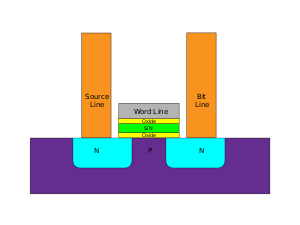
A SONOS memory cell is formed from a standard polysilicon N-channel MOSFET transistor with the addition of a small sliver of silicon nitride inserted inside the transistor's gate oxide. The sliver of nitride is non-conductive but contains a large number of charge trapping sites able to hold an electrostatic charge. The nitride layer is electrically isolated from the surrounding transistor, although charges stored on the nitride directly affect the conductivity of the underlying transistor channel. The oxide/nitride sandwich typically consists of a 2 nm thick oxide lower layer, a 5 nm thick silicon nitride middle layer, and a 5–10 nm oxide upper layer.
When the polysilicon control gate is biased positively, electrons from the transistor source and drain regions tunnel through the oxide layer and get trapped in the silicon nitride. This results in an energy barrier between the drain and the source, raising the threshold voltage Vt (the gate-source voltage necessary for current to flow through the transistor). The electrons can be removed again by applying a negative bias on the control gate.
A SONOS memory array is constructed by fabricating a grid of SONOS transistors which are connected by horizontal and vertical control lines (wordlines and bitlines) to peripheral circuitry such as address decoders and sense amplifiers. After storing or erasing the cell, the controller can measure the state of the cell by passing a small voltage across the source-drain nodes; if current flows the cell must be in the "no trapped electrons" state, which is considered a logical "1". If no current is seen the cell must be in the "trapped electrons" state, which is considered as "0" state. The needed voltages are normally about 2 V for the erased state, and around 4.5 V for the programmed state.
Comparison with Floating-Gate structure
Generally SONOS is very similar to traditional FG (floating gate) type memory cell,[1]:117 but hypothetically offers higher quality storage. This is due to the smooth homogeneity of the Si3N4 film compared with polycrystalline film which has tiny irregularities. Flash requires the construction of a very high-performance insulating barrier on the gate leads of its transistors, often requiring as many as nine different steps, whereas the oxide layering in SONOS can be more easily produced on existing lines and more easily combined with CMOS logic.
Additionally, traditional flash is less tolerant of oxide defects because a single shorting defect will discharge the entire polysilicon floating gate. The nitride in the SONOS structure is non-conductive, so a short only disturbs a localized patch of charge. Even with the introduction of new insulator technologies this has a definite "lower limit" around 7 to 12 nm, which means it is difficult for flash devices to scale smaller than about 45 nm linewidths. But, Intel-Micron group have realized 16 nm planar flash memory with traditional FG technology.[7]:13[8] SONOS, on the other hand, requires a very thin layer of insulator in order to work, making the gate area smaller than flash. This allows SONOS to scale to smaller linewidth, with recent examples being produced on 40 nm fabs and claims that it will scale to 20 nm.[9] The linewidth is directly related to the overall storage of the resulting device, and indirectly related to the cost; in theory, SONOS' better scalability will result in higher capacity devices at lower costs.
Additionally, the voltage needed to bias the gate during writing is much smaller than in traditional flash. In order to write flash, power is first built up in a separate device known as a charge pump, which multiplies the input voltage to between 9 V to 20 V. This process takes some time, meaning that writing to a flash cell is much slower than reading, often between 100 and 1000 times slower. The pulse of high power also degrades the cells slightly, meaning that flash devices can only be written to between 10,000 and 100,000 times, depending on the type. SONOS devices require much lower write voltages, typically 5–8 V, and do not degrade in the same way. SONOS does suffer from an unrelated problem, however, where electrons become strongly trapped in the ONO layer and cannot be removed again. Over long usage this can eventually lead to enough trapped electrons to permanently set the cell to the "0" state, similar to the problems in flash. However, in SONOS this requires on the order of a 100 thousands write/erase cycles,[10] 10 to 100 times worse compared with legacy FG memory cell.[11]
History
SONOS was first conceptualized in the 1960s. MONOS is realized in 1968 by a Westinghouse Electric Corporation.[12][13] In the early 1970s initial commercial devices were realized using PMOS transistors and a metal-nitride-oxide (MNOS) stack with a 45 nm nitride storage layer. These devices required up to 30V to operate. In 1977, Fairchild introduced one of SONOS cross sectional structured MOSFET with tunnel silicon dioxide of 30 Ångström thickness for EEPROM.[2] According to NCR Corporation's patent application in 1980, SONOS structure required +25 volts and −25 volts for writing and erasing, respectively.[14] It was improved to +12 V by PMOS-based MNOS (metal-nitride-oxide-semiconductor) structure.[15] By the early 1980s, polysilicon NMOS-based structures were in use with operating voltages under 20 V. By the late 1980s and early 1990s PMOS SONOS structures were demonstrating program/erase voltages in the range of 5–12 volts.[16] On the other hand, in 1980, Intel realized highly reliable EEPROM with double layerd polysilicon structure, which is named FLOTOX,[17] both for erase and write cycling endurance and for data retention term.[18] SONOS has been in the past produced by Philips Semiconductors, Spansion, Qimonda and Saifun Semiconductors.
Current efforts
In 2002, AMD and Fujitsu, formed as Spansion in 2003 and later merged with Cypress Semiconductor in 2014, developed a SONOS-like MirrorBit technology based on the license from Saifun Semiconductors, Ltd.'s NROM technology.[19][20][21] As of 2011 Cypress Semiconductor developed SONOS memories for multiple processes,[22] and started to sell them as IP to embed in other devices.[23] UMC has already used SONOS since 2006 [24] and has licensed Cypress for 40nm[25] and other nodes. Shanghai Huali Microelectronics Corporation (HLMC) has also announced[26] to be producing Cypress SONOS at 40nm and 55nm.
In 2006, Toshiba developed a new double tunneling layer technology with SONOS structure, which utilize Si9N10 silicon nitride.[27][28] Toshiba also researches MONOS ("Metal-Oxide-Nitride-Oxide-Silicon") structure for their 20 nm node NAND gate type flash memories.[29] Renesas Electronics uses MONOS structure in 40nm node era.[30][31]:5 which is the result of collaboration with TSMC.[32]
While other companies still use FG (floating gate) structure.[33]:50 For example, GlobalFoundries use floating-gate-based split-gate SuperFlash ESF3 cell for their 40nm products.[34] Some new structure for FG (floating gate) type flash memories are still intensively studied.[35] In 2016, GlobalFoundries developed FG-based 2.5V Embedded flash macro.[36] In 2017, Fujitsu announced to license FG-based ESF3/FLOTOX structure,[17][18] which is originally developed by Intel in 1980, from Silicon Storage Technology for their embedded non-volatile memory solutions.[37][38][39] As of 2016, Intel-Micron group have disclosed that they stayed traditional FG technology in their 3-dimensional NAND flash memory.[7] They also use FG technology for 16nm planar NAND flash.[8]
See also
References
- 1 2 Micheloni, Rino; Crippa, Luca; Marelli, Alessia (2010). Inside NAND Flash Memories (Google Books). Springer Science & Business Media. ISBN 9789048194315.
- 1 2 Chen, P. C. Y. (1977). "Threshold-alterable Si-gate MOS devices". IEEE Transactions on Electron Devices. 24 (5): 584–586. doi:10.1109/T-ED.1977.18783. ISSN 0018-9383.
- ↑ Chen, S. C.; Chang, T. C.; Liu, P. T.; Wu, Y. C.; Lin, P. S.; Tseng, B. H.; Shy, J. H.; Sze, S. M.; Chang, C. Y.; Lien, C. H. (2007). "A Novel Nanowire Channel Poly-Si TFT Functioning as Transistor and Nonvolatile SONOS Memory (reprint of ResearchGate)". IEEE Electron Device Letters. 28 (9): 809–811. doi:10.1109/LED.2007.903885. ISSN 0741-3106.
- ↑ Lee, M. C.; Wong, H. Y. (2013). "Charge Loss Mechanisms of Nitride-Based Charge Trap Flash Memory Devices (reprint on ReserchGate)" (PDF). IEEE Transactions on Electron Devices. 60 (10): 3256–3264. doi:10.1109/TED.2013.2279410. ISSN 0018-9383.
- ↑ Prince, Betty (2007). Emerging Memories: Technologies and Trends. Springer Science & Business Media. ISBN 9780306475535.
- ↑ Remond, I.; Akil, N. (May 2006). "Modeling of transient programming and erasing of SONOS non-volatile memories (reprint on CiteSeerX)". Technical Note PR-TN 2006/00368. Koninklijke Philips Electronics N.V.
- 1 2 "NAND Flash Memory Roadmap" (PDF). TechInsights Inc. June 2016.
- 1 2 CHOE, JEONGDONG. "Deep dive into the Intel/Micron 3D 32L FG-NAND". www.techinsights.com.
- ↑ Samsung unwraps 40nm "charge trap flash" device // ElectroIQ, 2006-09
- ↑ Wang, S. Y.; Lue, H. T.; Hsu, T. H.; Du, P. Y.; Lai, S. C.; Hsiao, Y. H.; Hong, S. P.; Wu, M. T.; Hsu, F. H.; Lian, N. T.; Lu, C. P.; Hsieh, J. Y.; Yang, L. W.; Yang, T.; Chen, K. C.; Hsieh, K. Y.; Lu, C. Y. (2010). "A high-endurance (≫100K) BE-SONOS NAND flash with a robust nitrided tunnel oxide/si interface". 2010 IEEE International Reliability Physics Symposium: 951–955. doi:10.1109/IRPS.2010.5488698.
- ↑ Arai, F.; Maruyama, T.; Shirota, R. (1998). "Extended data retention process technology for highly reliable flash EEPROMs of 10/sup 6/ to 10/sup 7/ W/E cycles". 1998 IEEE International Reliability Physics Symposium Proceedings. 36th Annual (Cat. No.98CH36173): 378–382. doi:10.1109/RELPHY.1998.670672.
- ↑ Dummer, G. W. A. (2013). Electronic Inventions and Discoveries: Electronics from Its Earliest Beginnings to the Present Day (Google Books). Elsevier. ISBN 9781483145211.
- ↑ Keshavan, B. V.; Lin, H. C. (October 1968). "MONOS memory element". 1968 International Electron Devices Meeting. 14: 140–142. doi:10.1109/IEDM.1968.188066.
- ↑
TRUDEL, L; DHAM, V (1980-09-11). "Application WO1981000790: Silicon gate non-volatile memory device". Google Patents. NCR Corporation.
The initialization procedure (steps 1, 4 and 7), i.e. obtaining the initial written and erased state threshold voltages, involved applying +25 volts for three seconds and -25 volts for three seconds, respectively, at room temperature to the gates of the memory FETs. Source, drain and substrate were all tied to ground during this initialization.
- ↑ TRUDEL, MURRAY L; LOCKWOOD, GEORGE C; EVANS, EVANS G (1980-10-01). "Patent US4353083: Low voltage nonvolatile memory device". Google Patents. NCR Corporation.
- ↑ White, Marvin (July 2000), "On the Go with SONOS", IEEE Circuits & Devices
- 1 2 Johnson, W.; Perlegos, G.; Renninger, A.; Kuhn, G.; Ranganath, T. (1980). "A 16Kb electrically erasable nonvolatile memory". 1980 IEEE International Solid-State Circuits Conference. Digest of Technical Papers. XXIII: 152–153. doi:10.1109/ISSCC.1980.1156030.
- 1 2
Euzent, B.; Boruta, N.; Lee, J.; Jenq, C. (1981). "Reliability Aspects of a Floating Gate E2 PROM". 19th International Reliability Physics Symposium: 11–16. doi:10.1109/IRPS.1981.362965.
The Intel 2816 uses the FLOTOX structure, which has been discussed in detail in the literaturel. Basically, it utilizes an oxide of less than 200A thick between the floating polysilicon gate and the N+ region as shown in Figure 1. - ↑ "AMD, FUJITSU AND SAIFUN ANNOUNCE COLLABORATION - News Room - FUJITSU". pr.fujitsu.com.
- ↑ Vogler, Debra (November 2007). "Spansion makes diversity play with SONOS-based MirrorBit technology | Solid State Technology". electroiq.com. Retrieved 23 March 2018.
- ↑ "Spansion Unveils Plans for SONOS-based MirrorBit(R) ORNAND(TM) Family". www.cypress.com. Spansion Inc.
- ↑ Ramkumar, Krishnaswamy; Jin, Bo (29 Sep 2011). "Advantages of SONOS memory for embedded flash technology". EE Times.
- ↑ Cypress SONOS Technology
- ↑ LaPedus, Mark (19 Apr 2006). "UMC fabs Sonos memory chip". EE Times.
- ↑ Cypress Press Release, 21 Jan 2015
- ↑ "HLMC and Cypress Announce Initial Production Milestone of Embedded Flash Using 55-Nanometer Low Power Process Technology with SONOS Flash". PRNewswire. 12 Apr 2017.
- ↑ Ohba, R.; Mitani, Y.; Sugiyama, N.; Fujita, S. (2006). "25 nm Planar Bulk SONOS-type Memory with Double Tunnel Junction". 2006 International Electron Devices Meeting: 1–4. doi:10.1109/IEDM.2006.346945.
- ↑ LaPedus, Mark (2007-12-12). "Toshiba puts new twist on SONOS | EE Times". EETimes.
- ↑ Sakamoto, W.; Yaegashi, T.; Okamura, T.; Toba, T.; Komiya, K.; Sakuma, K.; Matsunaga, Y.; Ishibashi, Y.; Nagashima, H.; Sugi, M.; Kawada, N.; Umemura, M.; Kondo, M.; Izumida, T.; Aoki, N.; Watanabe, T. (2009). "Reliability improvement in planar MONOS cell for 20nm-node multi-level NAND Flash memory and beyond". 2009 IEEE International Electron Devices Meeting (IEDM): 1–4. doi:10.1109/IEDM.2009.5424211.
- ↑ Kono, T.; Ito, T.; Tsuruda, T.; Nishiyama, T.; Nagasawa, T.; Ogawa, T.; Kawashima, Y.; Hidaka, H.; Yamauchi, T. (2013). "40nm embedded SG-MONOS flash macros for automotive with 160MHz random access for code and endurance over 10M cycles for data". 2013 IEEE International Solid-State Circuits Conference Digest of Technical Papers: 212–213. doi:10.1109/ISSCC.2013.6487704.
- ↑ Fischer, T.; Nam, B. G.; Chang, L.; Kuroda, T.; Pertijs, M. A. P. (2013). "Highlights of the ISSCC 2013 Processors and High Performance Digital Sessions" (PDF). IEEE Journal of Solid-State Circuits. 49 (1): 4–8. doi:10.1109/JSSC.2013.2284658. ISSN 0018-9200.
- ↑ Yoshida, Junko (2012-05-28). "Renesas, TSMC tout licensable MCU platform using 40-nm eFlash | EE Times". EETimes.
- ↑ Dimitrakis, Panagiotis (2017). Charge-Trapping Non-Volatile Memories: Volume 2--Emerging Materials and Structures (Google Books). Springer. ISBN 9783319487052.
- ↑ Luo, L. Q.; Teo, Z. Q.; Kong, Y. J.; Deng, F. X.; Liu, J. Q.; Zhang, F.; Cai, X. S.; Tan, K. M.; Lim, K. Y.; Khoo, P.; Jung, S. M.; Siah, S. Y.; Shum, D.; Wang, C. M.; Xing, J. C.; Liu, G. Y.; Diao, Y.; Lin, G. M.; Tee, L.; Lemke, S. M.; Ghazavi, P.; Liu, X.; Do, N.; Pey, K. L.; Shubhakar, K. (May 2016). "Functionality Demonstration of a High-Density 2.5V Self-Aligned Split-Gate NVM Cell Embedded into 40nm CMOS Logic Process for Automotive Microcontrollers (reprint on GlobalFoundaries)" (PDF). 2016 IEEE 8th International Memory Workshop (IMW): 1–4. doi:10.1109/IMW.2016.7495271. ISBN 978-1-4673-8833-7.
- ↑ Zhou, Ye; Han, Su-Ting; Yan, Yan; Huang, Long-Biao; Zhou, Li; Huang, Jing; Roy, V. A. L. (31 October 2013). "Solution processed molecular floating gate for flexible flash memories" (PDF). Scientific Reports. Macmillan Publishers Limited. 3 (1). doi:10.1038/srep03093. ISSN 2045-2322.
- ↑ Luo, L. Q.; Teo, Z. Q.; Kong, Y. J.; Deng, F. X.; Liu, J. Q.; Zhang, F.; Cai, X. S.; Tan, K. M.; Lim, K. Y.; Khoo, P.; Jung, S. M.; Siah, S. Y.; Shum, D.; Wang, C. M.; Xing, J. C.; Liu, G. Y.; Diao, Y.; Lin, G. M.; Tee, L.; Lemke, S. M.; Ghazavi, P.; Liu, X.; Do, N.; Pey, K. L.; Shubhakar, K. (May 2016). "Functionality Demonstration of a High-Density 2.5V Self-Aligned Split-Gate NVM Cell Embedded into 40nm CMOS Logic Process for Automotive Microcontrollers" (PDF). 2016 IEEE 8th International Memory Workshop (IMW): 1–4. doi:10.1109/IMW.2016.7495271.
- ↑ "Mie Fujitsu and SST Announce Automotive Platform Development on 40nm Technology : MIE FUJITSU SEMICONDUCTOR LIMITED". www.fujitsu.com. 2017-08-07.
- ↑ "Embedded Non-Volatile Memory Solutions : MIE FUJITSU SEMICONDUCTOR LIMITED". www.fujitsu.com. Fujitsu.
- ↑ Broome, Sarah. "Mie Fujitsu and SST Announce Automotive Platform Development on 40nm Technology". www.sst.com. Silicon Storage Technology.
External links
- Threshold-alterable Si-gate MOS devices | IEEE Xplore
- Characterization of scaled SONOS EEPROM memory devices for space and military systems | IEEE Xplore
- Gutmann (2001) papaer: "Data Remanence in Semiconductor Devices" | USENIX