Surface-conduction electron-emitter display

A surface-conduction electron-emitter display (SED) is a display technology for flat panel displays developed by a number of companies. SEDs use nanoscopic-scale electron emitters to energize colored phosphors and produce an image. In a general sense, an SED consists of a matrix of tiny cathode ray tubes, each "tube" forming a single sub-pixel on the screen, grouped in threes to form red-green-blue (RGB) pixels. SEDs combine the advantages of CRTs, namely their high contrast ratios, wide viewing angles and very fast response times, with the packaging advantages of LCD and other flat panel displays. They also use much less power than an LCD television of the same size.
After considerable time and effort in the early and mid-2000s, SED efforts started winding down in 2009 as LCD became the dominant technology. In August 2010, Canon announced they were shutting down their joint effort to develop SEDs commercially, signalling the end of development efforts.[1] SEDs are closely related to another developing display technology, the field emission display, or FED, differing primarily in the details of the electron emitters. Sony, the main backer of FED, has similarly backed off from their development efforts.[2]
Description
A conventional cathode ray tube (CRT) is powered by an electron gun, essentially an open-ended vacuum tube. At one end of the gun electrons are produced by "boiling" them off a metal filament, which requires relatively high currents and consumes a large proportion of the CRT's power. The electrons are then accelerated and focused into a fast-moving beam, flowing forward towards the screen. Electromagnets surrounding the gun end of the tube are used to steer the beam as it travels forward, allowing the beam to be scanned across the screen to produce a 2D display. When the fast-moving electrons strike phosphor on the back of the screen, light is produced. Color images are produced by painting the screen with spots or stripes of three colored phosphors, one each for red, green and blue (RGB). When viewed from a distance, the spots, known as "sub-pixels", blend together in the eye to produce a single picture element known as a pixel.
The SED replaces the single gun of a conventional CRT with a grid of nanoscopic emitters, one for each sub-pixel of the display. The emitter apparatus consists of a thin slit across which electrons jump when powered with high-voltage gradients. Due to the nanoscopic size of the slits, the required field can correspond to a potential on the order of tens of volts. A few of the electrons, on the order of 3%, impact with slit material on the far side and are scattered out of the emitter surface. A second field, applied externally, accelerates these scattered electrons towards the screen. Production of this field requires kilovolt potentials, but is a constant field requiring no switching, so the electronics that produce it are quite simple.
Each emitter is aligned behind a colored phosphor dot, and the accelerated electrons strike the dot and cause it to give off light in a fashion identical to a conventional CRT. Since each dot on the screen is lit by a single emitter, there is no need to steer or direct the beam as there is in an CRT. The quantum tunneling effect which emits electrons across the slits is highly non-linear, and the emission process tends to be fully on or off for any given voltage. This allows the selection of particular emitters by powering a single horizontal row on the screen and then powering all of the needed vertical columns at the same time, thereby powering the selected emitters. The half power received by the rest of the emitters on the row is too small to cause emission, even when combined with voltage leaking from active emitters beside them. This allows SED displays to work without an active matrix of thin-film transistors that LCDs and similar displays require in order to precisely select every sub-pixel, and further reduces the complexity of the emitter array. However, this also means that changes in voltage cannot be used to control the brightness of the resulting pixels. Instead, the emitters are rapidly turned on and off using pulse width modulation, so that the total brightness of a spot in any given time can be controlled.[3]
SED screens consist of two glass sheets separated by a few millimeters, the rear layer supporting the emitters and the front the phosphors. The front is easily prepared using methods similar to existing CRT systems; the phosphors are painted onto the screen using a variety of silkscreen or similar technologies, and then covered with a thin layer of aluminum to make the screen visibly opaque and provide an electrical return path for the electrons once they strike the screen. In the SED, this layer also serves as the front electrode that accelerates the electrons toward the screen, which is held at a constant high voltage relative to the switching grid. As is the case with modern CRT's, a dark mask is applied to the glass before the phosphor is painted on, to give the screen a dark charcoal grey color and improve contrast ratio.
Creating the rear layer with the emitters is a multi-step process. First, a matrix of silver wires is printed on the screen to form the rows or columns, an insulator is added, and then the columns or rows are deposited on top of that. Electrodes are added into this array, typically using platinum, leaving a gap of about 60 micrometres between the columns. Next, square pads of palladium oxide (PdO) only 20 nm thick are deposited into the gaps between the electrodes, connecting to them to supply power. A small slit is cut into the pad in the middle by repeatedly pulsing high currents though them. The resulting erosion causes a gap to form. The gap in the pad forms the emitter. The width of the gap has to be tightly controlled in order to work properly, and this proved difficult to control in practice.
Modern SEDs add another step that greatly eases production. The pads are deposited with a much larger gap between them, as much as 50 nm, which allows them to be added directly using technology adapted from inkjet printers. The entire screen is then placed in an organic gas and pulses of electricity are sent through the pads. Carbon in the gas is pulled onto the edges of the slit in the PdO squares, forming thin films that extend vertically off the tops of the gaps and grow toward each other at a slight angle. This process is self-limiting; if the gap gets too small the pulses erode the carbon, so the gap width can be controlled to produce a fairly constant 5 nm slit between them.
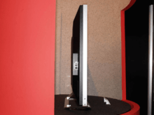
Since the screen needs to be held in a vacuum in order to work, there is a large inward force on the glass surfaces due to the surrounding atmospheric pressure. Because the emitters are laid out in vertical columns, there is a space between each column where there is no phosphor, normally above the column power lines. SEDs use this space to place thin sheets or rods on top of the conductors which keep the two glass surfaces apart. A series of these is used to reinforce the screen over its entire surface, which greatly reduces the needed strength of the glass itself.[3] A CRT has no place for similar reinforcements, so the glass at the front screen has to be thick enough to support all the pressure. SEDs are thus much thinner and lighter than CRTs.
Comparison
The primary large-screen television technology being deployed in the 2000s is the liquid crystal display televisions. SEDs are aimed at the same market segment.
LCDs do not directly produce light, and have to be back-lit using cold cathode fluorescent lamps (CCFLs) or high-power LEDs. The light is first passed through a polarizer, which cuts out half of the light. It then passes through the LCD layer, which selectively reduces the output for each sub-pixel. In front of the LCD shutters are small colored filters, one for each RGB sub-pixel. Since the colored filters cut out all but a narrow band of the white light, the amount of light that reaches the viewer is always less than 1/3 of what left the polarizer. Since the color gamut is produced by selectively reducing the output for certain colors, in practice much less light makes it through to the view, about 8 to 10% on average.[4] In spite of using highly efficient light sources, an LCD uses more power than a CRT of the same size.[5]
LCD shutters consist of an encapsulated liquid that changes its polarization in response to an applied electrical field. The response is fairly linear, so even a small amount of leaked power reaching the surrounding shutters causes the image to become blurry. To counteract this effect, and improve switching speed, LCDs use an Active matrix addressing of transparent thin-film transistors to directly switch each shutter. This adds complexity to the LCD screen and makes them more difficult to manufacture. The shutters are not perfect and allow light to leak through, which reduces both relative brightness and color gamut. Additionally, the use of a polarizer, to create the shutter, limits the viewing angles where a visually indistinguishable contrast-ratio experience may be had. Most importantly, the switching process takes some time, on the order of milliseconds, which leads to blurring of fast moving scenes. Massive investment in the LCD manufacturing process has addressed most of these issues, but no single LCD-based solution has proven able to overcome all of the aforementioned issues.
The SED produces light directly on its front surface. Scenes are lit only on those pixels that require it, and only to the amount of brightness they require. In spite of the light generating process being less efficient than CCFLs or LEDs, the overall power efficiency of an SED is about ten times better than a LCD of the same size. SEDs are also much less complex in overall terms – they lack the active matrix layer, backlighting section, color filters and the driver electronics that adjusts for various disadvantages in the LCD shuttering process. Despite having two glass layers instead of one in a typical LCD, this reduction in overall complexity makes SEDs similar in weight and size as LCDs.
Canon's 55" prototype SED offered bright images of 450 cd/m2, 50,000:1 contrast ratios, and a response time of less than 1 ms.[6] Canon has stated that production versions would improve the response time to 0.2 ms and 100,000:1 contrast ratios.[7] SEDs can be viewed from extremely wide angles without any effect on the quality of the image. In comparison, a modern LCD televisions like the Sony KDL-52W4100 claims to offer 30,000:1 contrast ratios, but this uses the "dynamic contrast" measurement, and the "on-screen contrast ratio" is a more realistic 3,000:1.[8] Contrast ratios of LCD televisions are widely inflated in this manner.[9] The same set claims to offer viewing angles of 178 degrees, but the useful viewing angles are much narrower, and beyond that, both color gamut and contrast ratio changes. Sony does not quote their response times, but 4 ms is common for larger sets, although this is also a dynamic measurement that only works for certain transitions.
SEDs are very closely related to the field emission display (FED), differing only in the details of the emitter. FEDs use small spots containing hundreds of carbon nanotubes whose sharp tips give off electrons when placed in a strong electrical field. FEDs suffer from erosion of the emitters, and require extremely high vacuum in order to operate. For this reason, industry observers generally state that the SED is a more practical design. FEDs have one advantage the SED does not offer; since each sub-pixel has hundreds of emitters, "dead" emitters can be corrected by applying slightly more power to the working ones. In theory, this could increase yields because the chance of a pixel being completely dead is very low, and the chance that a screen has many dead pixels is greatly reduced.[3] Sony has demonstrated a 26" FED drawing only 12 W showing a bright scene,[10] SEDs should be even lower powered.[3] Throughout the flat-screen introduction, several other technologies had been vying with LCDs and PDPs for market acceptance. Among these were the SED, the FED, and the organic light-emitting diode system that uses printable LEDs. All of these shared the advantages of low power use, excellent contrast ratio and color gamut, fast response times and wide viewable angles. All of them also shared the problem of scaling up manufacturing to produce large screens. Example systems of limited size, generally 13", have been shown for several years and are available for limited sales, but wide-scale production has not started on any of these alternatives.
History
Canon began SED research in 1986.[11] Their early research used PdO electrodes without the carbon films on top, but controlling the slit width proved difficult. At the time there were a number of flat-screen technologies in early development, and the only one close to commercialization was the plasma display panel (PDP), which had numerous disadvantages – manufacturing cost and energy use among them. LCDs were not suitable for larger screen sizes due to low yields and complex manufacturing.
In 2004 Canon signed an agreement with Toshiba to create a joint venture to continue development of SED technology, forming "SED Ltd." Toshiba introduced new technology to pattern the conductors underlying the emitters using technologies adapted from inkjet printers. At the time both companies claimed that production was slated to begin in 2005. Both Canon and Toshiba started displaying prototype units at trade shows during 2006, including 55" and 36" units from Canon, and a 42" unit from Toshiba. They were widely lauded in the press for their image quality, saying it was "something that must be seen to believe[d]."[12]
However, by this point Canon's SED introduction date had already slipped several times. It was first claimed it would go into production in 1999. This was pushed back to 2005 after the joint agreement, and then again into 2007 after the first demonstrations at CES and other shows.
In October 2006, Toshiba's president announced the company plans to begin full production of 55-inch SED TVs in July 2007 at its recently built SED volume-production facility in Himeji.[13]
In December 2006, Toshiba President and Chief Executive Atsutoshi Nishida said Toshiba was on track to mass-produce SED TV sets in cooperation with Canon by 2008. He said the company planned to start small-output production in the fall of 2007,[14] but they do not expect SED displays to become a commodity and will not release the technology to the consumer market because of its expected high price, reserving it solely for professional broadcasting applications.[15]
Also, in December 2006 it was revealed that one reason for the delay was a lawsuit brought against Canon by Applied Nanotech. On 25 May 2007, Canon announced that the prolonged litigation would postpone the launch of SED televisions, and a new launch date would be announced at some date in the future.[16]
Applied Nanotech, a subsidiary of Nano-Proprietary, holds a number of patents related to FED and SED manufacturing. They had sold Canon a perpetual license for a coating technology used in their newer carbon-based emitter structure. Applied Nanotech claimed that Canon's agreement with Toshiba amounted to an illegal technology transfer, and a separate agreement would have to be reached. They first approached the problem in April 2005.[17]
Canon responded to the lawsuit with several actions. On 12 January 2007 they announced that they would buy all of Toshiba's shares in SED Inc. in order to eliminate Toshiba's involvement in the venture.[18] They also started re-working their existing RE40,062 patent filing in order to remove any of Applied Nanotech's technologies from their system. The modified patent was issued on 12 February 2008.[19]
On 22 February 2007, the U.S. District Court for the Western District of Texas, a district widely known for agreeing with patent holders in intellectual property cases, ruled in a summary judgment that Canon had violated its agreement by forming a joint television venture with Toshiba.[20] However, on 2 May 2007 a jury ruled that no additional damages beyond the $5.5m fee for the original licensing contract were due.[21][22]
On 25 July 2008, the U.S. Court of Appeals for the 5th Circuit reversed the lower court's decision and provided that Canon's "irrevocable and perpetual" non-exclusive licence was still enforceable and covers Canon's restructured subsidiary SED.[23] On 2 December 2008, Applied Nanotech dropped the lawsuit, stating that continuing the lawsuit "would probably be a futile effort".[17]
In spite of their legal success, Canon announced at the same time that the financial crisis of 2008 was making introduction of the sets far from certain, going so far as to say they would not be launching the product at that time "because people would laugh at them".[17]
Canon also had an ongoing OLED development process that started in the midst of the lawsuit. In 2007 they announced a joint deal to form "Hitachi Displays Ltd.", with Matsushita and Canon each taking a 24.9% share of Hitachi's existing subsidiary. Canon later announced that they were purchasing Tokki Corp, a maker of OLED fabrication equipment.[24]
In April 2009 during NAB 2009, Peter Putman was quoted as saying "I was asked on more than one occasion about the chances of Canon's SED making a comeback, something I would not have bet money on after the Nano Technologies licensing debacle. However, a source within Canon told me at the show that the SED is still very much alive as a pro monitor technology. Indeed, a Canon SED engineer from Japan was quietly making the rounds in the Las Vegas Convention Center to scope out the competition."[25]
Canon officially announced on 25 May 2010 the end of the development of SED TVs for the home consumer market,[26] but indicated that they will continue development for commercial applications like medical equipment. On 18 August 2010, Canon decided to liquidate SED Inc.,[27] a consolidated subsidiary of Canon Inc. developing SED technology, citing difficulties to secure appropriate profitability and effectively ending hopes to one day see SED TVs in the living room.
See also
Notes
- ↑ Martyn Williams, "Canon signals end of the road for SED TV dreams", IDG News Service, 19 August 2010
- ↑ Serkan Toto, "FED: Sony calls it quits, basically burying the technology as a whole", CrunchGear, 31 Mar 2009
- 1 2 3 4 Closer
- ↑ 3M, "Vikuiti: Specialty Display Products"
- ↑ Jose Fermoso, "California Proposes Ban on Energy-Hogging HDTVs Starting in 2011", Wired, 29 March 2009
- ↑ Richard Lawler, 1080p "55-inch SED HDTVs on the way in '08", engadget, 3 October 2006
- ↑ Takuya Otani, "SED Panel Contrast Ratio Boosted to 100,000:1", Nikkei Electronics, 21 April 2005
- ↑ Sony, "KDL-52W4100, 52 BRAVIA W Series LCD Flat Panel HDTV"
- ↑ George Ou, "How LCD makers inflate their contrast ratio scores", ZDnet, 23 December 2007
- ↑ "Sony to Debut FED In 2009, Insists on Confusing Consumers With Yet Another Display Technology", gizmondo, 9 April 2007
- ↑ Standing
- ↑ Vincent Nguyen, SED Next-Generation Flat-Screen Display, SlashGear, 19 October 2006
- ↑ "Toshiba eyes mass SED TV output in early '08". MarketWatch, Inc. 2006-06-20. Retrieved 2006-09-29.
- ↑ Kim, Yun-Hee (2006-12-22). "Toshiba, Canon work on displays". Dow Jones & Company, Inc. Retrieved 2006-12-22.
- ↑ SED Won't Become Commodity -- Toshiba's President Nishida Said at Year-End Press Gathering December 25, 2006 Masao Oonishi, Nikkei Microdevices
- ↑ "Notice Regarding Launch of SED TVs.", Canon Inc., 25 May 2007
- 1 2 3 Robin Harding, "Canon clear to launch new type of TV", Financial Times, 2 December 2008
- ↑ "SED Inc. to become wholly owned subsidiary of Canon Inc." Archived 2007-01-14 at the Wayback Machine., Canon Inc., 12 January 2007
- ↑ RE40,062
- ↑ "Judge rules against Canon in nanotube TV case". CNET. 2007-02-22. Archived from the original on 2007-02-25. Retrieved 2013-08-22.
- ↑ "Nano-Proprietary, Inc. Announces Verdict in Canon Litigation". 2007-05-03. Retrieved 2007-05-06.
- ↑ "Notice Regarding Litigation with Nano-Proprietary Involving SED". 2007-05-07. Archived from the original on 2007-05-09. Retrieved 2007-05-07.
- ↑ "Appeal's Court Ruling on No. 07-50640"
- ↑ "Canon to take majority stake in Tokki for $69 mln", Reuters, 13 November 2007
- ↑ "NAB 2009: The Season Of Their Discontent". 2009-04-27. Archived from the original on 2009-05-02. Retrieved 2009-04-27.
- ↑ "Canon to freeze development of home-use SED TVs", Reuters, 25 May 2010
- ↑ "Notice regarding liquidation of subsidiary", Canon Inc., 18 August 2010
Bibliography
- Richard Fink, "A closer look at SED, FED technologies", EE Times-Asia, August 16–31, 2007, pp. 1–4
- Peter Putman, "Standing in the shadows" , HDTVexpert, 8 March 2006
Patents
- U.S. Patent RE40,062, "Display device with electron-emitting device with electron-emitting region", Seishiro Yoshioka et al./Canon Kabushiki Kaisha, Filed 2 June 2000, Re-issued 12 Feb 2008
Further reading
- "Funding for organic-LED technology, patent disputes, and more", Nature Photonics, Volume 1 Number 5 (2007), pg. 278
External links
| Look up surface-conduction electron-emitter display in Wiktionary, the free dictionary. |
| Wikinews has related news: Canon Inc. to buy the stake of Toshiba in their joint venture |