Field-programmable gate array
A field-programmable gate array (FPGA) is an integrated circuit designed to be configured by a customer or a designer after manufacturing – hence "field-programmable". The FPGA configuration is generally specified using a hardware description language (HDL), similar to that used for an application-specific integrated circuit (ASIC). Circuit diagrams were previously used to specify the configuration, but this is increasingly rare due to the advent of electronic design automation tools.
FPGAs contain an array of programmable logic blocks, and a hierarchy of reconfigurable interconnects that allow the blocks to be "wired together", like many logic gates that can be inter-wired in different configurations. Logic blocks can be configured to perform complex combinational functions, or merely simple logic gates like AND and XOR. In most FPGAs, logic blocks also include memory elements, which may be simple flip-flops or more complete blocks of memory.[1] Many FPGAs can be reprogrammed to implement different logic functions,[2] allowing flexible reconfigurable computing as performed in computer software.
Technical design
Contemporary field-programmable gate arrays (FPGAs) have large resources of logic gates and RAM blocks to implement complex digital computations.[2] As FPGA designs employ very fast I/O rates and bidirectional data buses, it becomes a challenge to verify correct timing of valid data within setup time and hold time. Floor planning enables resource allocation within FPGAs to meet these time constraints. FPGAs can be used to implement any logical function that an ASIC can perform. The ability to update the functionality after shipping, partial re-configuration of a portion of the design[3] and the low non-recurring engineering costs relative to an ASIC design (notwithstanding the generally higher unit cost), offer advantages for many applications.[1]
Some FPGAs have analog features in addition to digital functions. The most common analog feature is a programmable slew rate on each output pin, allowing the engineer to set low rates on lightly loaded pins that would otherwise ring or couple unacceptably, and to set higher rates on heavily loaded pins on high-speed channels that would otherwise run too slowly.[4][5] Also common are quartz-crystal oscillators, on-chip resistance-capacitance oscillators, and phase-locked loops with embedded voltage-controlled oscillators used for clock generation and management and for high-speed serializer-deserializer (SERDES) transmit clocks and receiver clock recovery. Fairly common are differential comparators on input pins designed to be connected to differential signaling channels. A few "mixed signal FPGAs" have integrated peripheral analog-to-digital converters (ADCs) and digital-to-analog converters (DACs) with analog signal conditioning blocks allowing them to operate as a system-on-a-chip.[6] Such devices blur the line between an FPGA, which carries digital ones and zeros on its internal programmable interconnect fabric, and field-programmable analog array (FPAA), which carries analog values on its internal programmable interconnect fabric.
History
The FPGA industry sprouted from programmable read-only memory (PROM) and programmable logic devices (PLDs). PROMs and PLDs both had the option of being programmed in batches in a factory or in the field (field-programmable). However, programmable logic was hard-wired between logic gates.[7]
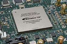
Altera was founded in 1983 and delivered the industry's first reprogrammable logic device in 1984 – the EP300 – which featured a quartz window in the package that allowed users to shine an ultra-violet lamp on the die to erase the EPROM cells that held the device configuration.[8] As of December 2015, it was acquired by Intel.
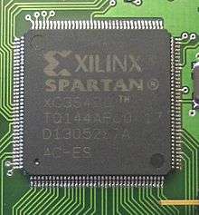
Xilinx co-founders Ross Freeman and Bernard Vonderschmitt invented the first commercially viable field-programmable gate array in 1985 – the XC2064.[9][10] The XC2064 had programmable gates and programmable interconnects between gates, the beginnings of a new technology and market.[11] The XC2064 had 64 configurable logic blocks (CLBs), with two three-input lookup tables (LUTs).[12] More than 20 years later, Freeman was entered into the National Inventors Hall of Fame for his invention.[13][14]
In 1987, the Naval Surface Warfare Center funded an experiment proposed by Steve Casselman to develop a computer that would implement 600,000 reprogrammable gates. Casselman was successful and a patent related to the system was issued in 1992.[7]
Altera and Xilinx continued unchallenged and quickly grew from 1985 to the mid-1990s, when competitors sprouted up, eroding significant market share. By 1993, Actel (now Microsemi) was serving about 18 percent of the market.[11] By 2013, Altera (31 percent), Actel (10 percent) and Xilinx (36 percent) together represented approximately 77 percent of the FPGA market.[15]
The 1990s were a period of rapid growth for FPGAs, both in circuit sophistication and the volume of production. In the early 1990s, FPGAs were primarily used in telecommunications and networking. By the end of the decade, FPGAs found their way into consumer, automotive, and industrial applications.[16]
21st century developments
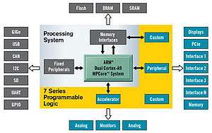
A recent trend has been to take the coarse-grained architectural approach a step further by combining the logic blocks and interconnects of traditional FPGAs with embedded microprocessors and related peripherals to form a complete "system on a programmable chip". This work mirrors the architecture created by Ron Perlof and Hana Potash of Burroughs Advanced Systems Group in 1982 which combined a reconfigurable CPU architecture on a single chip called the SB24. Examples of such hybrid technologies can be found in the Xilinx Zynq-7000 All Programmable SoC,[17] which includes a 1.0 GHz dual-core ARM Cortex-A9 MPCore processor embedded within the FPGA's logic fabric[18] or in the Altera Arria V FPGA, which includes an 800 MHz dual-core ARM Cortex-A9 MPCore. The Atmel FPSLIC is another such device, which uses an AVR processor in combination with Atmel's programmable logic architecture. The Microsemi SmartFusion devices incorporate an ARM Cortex-M3 hard processor core (with up to 512 kB of flash and 64 kB of RAM) and analog peripherals such as a multi-channel ADC and DACs to their flash-based FPGA fabric.
An alternate approach to using hard-macro processors is to make use of soft processor IP cores that are implemented within the FPGA logic. Nios II, MicroBlaze and Mico32 are examples of popular softcore processors. Many modern FPGAs are programmed at "run time", and this is leading to the idea of reconfigurable computing or reconfigurable systems – CPUs that reconfigure themselves to suit the task at hand. Additionally, new, non-FPGA architectures are beginning to emerge. Software-configurable microprocessors such as the Stretch S5000 adopt a hybrid approach by providing an array of processor cores and FPGA-like programmable cores on the same chip.
Companies like Microsoft have started to use FPGAs to accelerate high-performance, computationally intensive systems (like the data centers that operate their Bing search engine), due to the performance per watt advantage FPGAs deliver.[19] Microsoft began using FPGAs to accelerate Bing in 2014, and in 2018 began deploying FPGAs across other data center workloads for their Azure cloud computing platform.[20]
Timelines
Gates
Market size
Design starts
A design start is a new custom design for implementation on an FPGA.
Comparisons
Historically, FPGAs have been slower, less energy efficient and generally achieved less functionality than their fixed ASIC counterparts. An older study showed that designs implemented on FPGAs need on average 40 times as much area, draw 12 times as much dynamic power, and run at one third the speed of corresponding ASIC implementations. More recently, FPGAs such as the Xilinx Virtex-7 or the Altera Stratix 5 have come to rival corresponding ASIC and ASSP solutions by providing significantly reduced power usage, increased speed, lower materials cost, minimal implementation real-estate, and increased possibilities for re-configuration 'on-the-fly'. Where previously a design may have included 6 to 10 ASICs, the same design can now be achieved using only one FPGA.[26]
Advantages of FPGAs include the ability to re-program in the field to fix bugs, and may include a shorter time to market and lower non-recurring engineering costs. Vendors can also take a middle road by developing their hardware on ordinary FPGAs, but manufacture their final version as an ASIC so that it can no longer be modified after the design has been committed. This is also known as FPGA prototyping.
Xilinx claims that several market and technology dynamics are changing the ASIC/FPGA paradigm:[27]
- Integrated circuit development costs are rising aggressively
- ASIC complexity has lengthened development time
- R&D resources and headcount are decreasing
- Revenue losses for slow time-to-market are increasing
- Financial constraints in a poor economy are driving low-cost technologies.
These trends make FPGAs a better alternative than ASICs for a larger number of higher-volume applications than they have been historically used for, to which the company attributes the growing number of FPGA design starts (see § History).[27]
Some FPGAs have the capability of partial re-configuration that lets one portion of the device be re-programmed while other portions continue running.
Complex programmable logic devices (CPLD)
The primary differences between complex programmable logic devices (CPLDs) and FPGAs are architectural. A CPLD has a somewhat restrictive structure consisting of one or more programmable sum-of-products logic arrays feeding a relatively small number of clocked registers. The result of this is less flexibility, with the advantage of more predictable timing delays and a higher logic-to-interconnect ratio. The FPGA architectures, on the other hand, are dominated by interconnect. This makes them far more flexible (in terms of the range of designs that are practical for implementation within them) but also far more complex to design for.
In practice, the distinction between FPGAs and CPLDs is often one of size as FPGAs are usually much larger in terms of resources than CPLDs. Typically only FPGAs contain more complex embedded functions such as adders, multipliers, memory, and serializer/deserializers. Another common distinction is that CPLDs contain embedded flash memory to store their configuration while FPGAs usually, but not always, require external non-volatile memory.
When a design requires simple glue logic or similar functionality to existing IP cores without much need for changes, or when you need an instant-on circuit, CPLDs are generally preferred. For most other applications FPGAs are generally preferred. Sometimes both CPLDs and FPGAs are used in a single system design. In those designs, CPLDs generally perform glue logic functions as mentioned before and are responsible for “booting” the FPGA as well as controlling reset and boot sequence of the complete board. Therefore, depending on the application it may be judicious to use both FPGAs and CPLDs in a single design.[28]
Security considerations
With respect to security, FPGAs have both advantages and disadvantages as compared to ASICs or secure microprocessors. FPGAs' flexibility makes malicious modifications during fabrication a lower risk.[29] Previously, for many FPGAs, the design bitstream was exposed while the FPGA loads it from external memory (typically on every power-on). All major FPGA vendors now offer a spectrum of security solutions to designers such as bitstream encryption and authentication. For example, Altera and Xilinx offer AES (up to 256 bit) encryption for bitstreams stored in an external flash memory.
FPGAs that store their configuration internally in nonvolatile flash memory, such as Microsemi's ProAsic 3 or Lattice's XP2 programmable devices, do not expose the bitstream and do not need encryption. In addition, flash memory for a lookup table provides single event upset protection for space applications.. Customers wanting a higher guarantee of tamper resistance can use write-once, Antifuse FPGAs from vendors such as Microsemi.
With its Stratix 10 FPGAs and SoCs, Altera introduced a Secure Device Manager and physically uncloneable functions to provide high levels of protection against physical attacks.[30]
In 2012 researchers Sergei Skorobogatov and Christopher Woods demonstrated that FPGAs can be vulnerable to hostile intent. They discovered a critical backdoor vulnerability had been manufactured in silicon as part of the Actel/Microsemi ProAsic 3 making it vulnerable on many levels such as reprogramming crypto and access keys, accessing unencrypted bitstream, modifying low-level silicon features, and extracting configuration data.[31]
Applications
A FPGA can be used to solve any problem which is computable. This is trivially proven by the fact FPGA can be used to implement a soft microprocessor, such as the Xilinx MicroBlaze or Altera Nios II. Their advantage lies in that they are sometimes significantly faster for some applications because of their parallel nature and optimality in terms of the number of gates used for a certain process.[32]
FPGAs originally began as competitors to CPLDs to implement glue logic for PCBs. As their size, capabilities, and speed increased, they took over additional functions to the point where some are now marketed as full systems on chips (SoCs). Particularly with the introduction of dedicated multipliers into FPGA architectures in the late 1990s, applications which had traditionally been the sole reserve of DSPs began to incorporate FPGAs instead.[33][34]
Another trend in the use of FPGAs is hardware acceleration, where one can use the FPGA to accelerate certain parts of an algorithm and share part of the computation between the FPGA and a generic processor.[2] The search engine Bing is noted for adopting FPGA acceleration for its search algorithm in 2014.[35] As of 2018, FPGAs are seeing increased use as AI accelerators including Microsoft's so-termed "Project Catapult"[20] and for accelerating artificial neural networks for machine learning applications.
Traditionally, FPGAs have been reserved for specific vertical applications where the volume of production is small. For these low-volume applications, the premium that companies pay in hardware cost per unit for a programmable chip is more affordable than the development resources spent on creating an ASIC. As of 2017, new cost and performance dynamics have broadened the range of viable applications.
Common FPGA Applications:
- Aerospace and Defense
- Avionics/DO-254
- Communications
- Missiles & Munitions
- Secure Solutions
- Space
- Audio
- Connectivity Solutions
- Portable Electronics
- Software-Defined Radio
- Digital Signal Processing (DSP)
- Speech Recognition
- Automotive
- High Resolution Video
- Image Processing
- Vehicle Networking and Connectivity
- Automotive Infotainment
- Bioinformatics
- Broadcast
- Real-Time Video Engine
- EdgeQAM
- Encoders
- Displays
- Switches and Routers
- Consumer Electronics
- Digital Displays
- Digital Cameras
- Multi-function Printers
- Portable Electronics
- Set-top Boxes
- Flash Cartridges
- Data Center
- High Performance Computing
- Servers
- Super Computers
- SIGINT Systems
- High-end RADARs
- High-end Beam Forming Systems
- Data Mining Systems
- Industrial
- Industrial Imaging
- Industrial Networking
- Motor Control
- Integrated Circuit Design
- ASIC Prototyping
- Computer Hardware Emulation
- Medical
- Scientific Instruments
- Lock-in amplifiers
- Boxcar averagers
- Phase-locked loops
- Radio Astronomy
- Security
- Industrial Imaging
- Secure Solutions
- Hardware security module[36]
- Image Processing
- Video & Image Processing
- High Resolution Video
- Video Over IP Gateway
- Digital Displays
- Industrial Imaging
- Computer Vision
- Wired Communications
- Optical Transport Networks
- Network Processing
- Connectivity Interfaces
- Wireless Communications
- Baseband
- Connectivity Interfaces
- Mobile Backhaul
- Radio
Architecture
Logic blocks
The most common FPGA architecture[1] consists of an array of logic blocks (called configurable logic block, CLB, or logic array block, LAB, depending on vendor), I/O pads, and routing channels. Generally, all the routing channels have the same width (number of wires). Multiple I/O pads may fit into the height of one row or the width of one column in the array.
An application circuit must be mapped into an FPGA with adequate resources. While the number of CLBs/LABs and I/Os required is easily determined from the design, the number of routing tracks needed may vary considerably even among designs with the same amount of logic. For example, a crossbar switch requires much more routing than a systolic array with the same gate count. Since unused routing tracks increase the cost (and decrease the performance) of the part without providing any benefit, FPGA manufacturers try to provide just enough tracks so that most designs that will fit in terms of lookup tables (LUTs) and I/Os can be routed. This is determined by estimates such as those derived from Rent's rule or by experiments with existing designs. As of 2018, network-on-chip architectures for routing and interconnection are being developed.
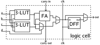
In general, a logic block consists of a few logical cells (called ALM, LE, slice etc.). A typical cell consists of a 4-input LUT, a full adder (FA) and a D-type flip-flop, as shown above. The LUTs are in this figure split into two 3-input LUTs. In normal mode those are combined into a 4-input LUT through the left multiplexer (mux). In arithmetic mode, their outputs are fed to the adder. The selection of mode is programmed into the middle multiplexer. The output can be either synchronous or asynchronous, depending on the programming of the mux to the right, in the figure example. In practice, entire or parts of the adder are stored as functions into the LUTs in order to save space.[37][38][39]
Hard blocks
Modern FPGA families expand upon the above capabilities to include higher level functionality fixed into the silicon. Having these common functions embedded into the silicon reduces the area required and gives those functions increased speed compared to building them from primitives. Examples of these include multipliers, generic DSP blocks, embedded processors, high speed I/O logic and embedded memories.
Higher-end FPGAs can contain high speed multi-gigabit transceivers and hard IP cores such as processor cores, Ethernet MACs, PCI/PCI Express controllers, and external memory controllers. These cores exist alongside the programmable fabric, but they are built out of transistors instead of LUTs so they have ASIC-level performance and power consumption without consuming a significant amount of fabric resources, leaving more of the fabric free for the application-specific logic. The multi-gigabit transceivers also contain high performance analog input and output circuitry along with high-speed serializers and deserializers, components which cannot be built out of LUTs. Higher-level PHY layer functionality such as line coding may or may not be implemented alongside the serializers and deserializers in hard logic, depending on the FPGA.
Clocking
Most of the circuitry built inside of an FPGA is synchronous circuitry that requires a clock signal. FPGAs contain dedicated global and regional routing networks for clock and reset so they can be delivered with minimal skew. Also, FPGAs generally contain analog PLL and/or DLL components to synthesize new clock frequencies as well as attenuate jitter. Complex designs can use multiple clocks with different frequency and phase relationships, each forming separate clock domains. These clock signals can be generated locally by an oscillator or they can be recovered from a high speed serial data stream. Care must be taken when building clock domain crossing circuitry to avoid metastability. FPGAs generally contain block RAMs that are capable of working as dual port RAMs with different clocks, aiding in the construction of building FIFOs and dual port buffers that connect differing clock domains.
3D architectures
To shrink the size and power consumption of FPGAs, vendors such as Tabula and Xilinx have introduced 3D or stacked architectures.[40][41] Following the introduction of its 28 nm 7-series FPGAs, Xilinx said that several of the highest-density parts in those FPGA product lines will be constructed using multiple dies in one package, employing technology developed for 3D construction and stacked-die assemblies.
Xilinx's approach stacks several (three or four) active FPGA dies side-by-side on a silicon interposer – a single piece of silicon that carries passive interconnect.[41][42] The multi-die construction also allows different parts of the FPGA to be created with different process technologies, as the process requirements are different between the FPGA fabric itself and the very high speed 28 Gbit/s serial transceivers. An FPGA built in this way is called a heterogeneous FPGA.[43]
Altera's heterogeneous approach involves using a single monolithic FPGA die and connecting other die/technologies to the FPGA using Intel's embedded multi-die interconnect bridge (EMIB) technology.[44]
Design and programming
To define the behavior of the FPGA, the user provides a design in a hardware description language (HDL) or as a schematic design. The HDL form is more suited to work with large structures because it's possible to specify high-level functional behavior rather than drawing every piece by hand. However, schematic entry can allow for easier visualization of a design.
Using an electronic design automation tool, a technology-mapped netlist is generated. The netlist can then be fit to the actual FPGA architecture using a process called place-and-route, usually performed by the FPGA company's proprietary place-and-route software. The user will validate the map, place and route results via timing analysis, simulation, and other verification and validation methodologies. Once the design and validation process is complete, the binary file generated, typically using the FPGA vendor's proprietary software, is used to (re-)configure the FPGA. This file is transferred to the FPGA/CPLD via a serial interface (JTAG) or to an external memory device like an EEPROM.
The most common HDLs are VHDL and Verilog as well as extensions such as SystemVerilog. However, in an attempt to reduce the complexity of designing in HDLs, which have been compared to the equivalent of assembly languages, there are moves to raise the abstraction level through the introduction of alternative languages. National Instruments' LabVIEW graphical programming language (sometimes referred to as "G") has an FPGA add-in module available to target and program FPGA hardware.
To simplify the design of complex systems in FPGAs, there exist libraries of predefined complex functions and circuits that have been tested and optimized to speed up the design process. These predefined circuits are commonly called IP cores, and are available from FPGA vendors and third-party IP suppliers (rarely free, and typically released under proprietary licenses). Other predefined circuits are available from developer communities such as OpenCores (typically released under free and open source licenses such as the GPL, BSD or similar license), and other sources. Such designs are known as "open-source hardware."
In a typical design flow, an FPGA application developer will simulate the design at multiple stages throughout the design process. Initially the RTL description in VHDL or Verilog is simulated by creating test benches to simulate the system and observe results. Then, after the synthesis engine has mapped the design to a netlist, the netlist is translated to a gate-level description where simulation is repeated to confirm the synthesis proceeded without errors. Finally the design is laid out in the FPGA at which point propagation delays can be added and the simulation run again with these values back-annotated onto the netlist.
More recently, OpenCL (Open Computing Language) is being used by programmers to take advantage of the performance and power efficiencies that FPGAs provide. OpenCL allows programmers to develop code in the C programming language and target FPGA functions as OpenCL kernels using OpenCL constructs.[45] For further information, see high-level synthesis and C to HDL.
Basic process technology types
- SRAM – based on static memory technology. In-system programmable and re-programmable. Requires external boot devices. CMOS. Currently in use. Notably, flash memory or EEPROM devices may often load contents into internal SRAM that controls routing and logic.
- Fuse – One-time programmable. Bipolar. Obsolete.
- Antifuse – One-time programmable. CMOS.
- PROM – Programmable Read-Only Memory technology. One-time programmable because of plastic packaging. Obsolete.
- EPROM – Erasable Programmable Read-Only Memory technology. One-time programmable but with window, can be erased with ultraviolet (UV) light. CMOS. Obsolete.
- EEPROM – Electrically Erasable Programmable Read-Only Memory technology. Can be erased, even in plastic packages. Some but not all EEPROM devices can be in-system programmed. CMOS.
- Flash – Flash-erase EPROM technology. Can be erased, even in plastic packages. Some but not all flash devices can be in-system programmed. Usually, a flash cell is smaller than an equivalent EEPROM cell and is therefore less expensive to manufacture. CMOS.
Major manufacturers
In 2016, long-time industry rivals Xilinx and Altera (now an Intel subsidiary) were the FPGA market leaders.[46] At that time, they controlled nearly 90 percent of the market.
Both Xilinx and Altera provide proprietary electronic design automation software for Windows and Linux (ISE/Vivado and Quartus) which enables engineers to design, analyze, simulate, and synthesize (compile) their designs.[47][48]
Other manufacturers include:
- Microchip:
- Lattice Semiconductor, which manufactures low-power SRAM-based FPGAs featuring integrated configuration flash, instant-on and live reconfiguration
- SiliconBlue Technologies, which provides extremely low power SRAM-based FPGAs with optional integrated nonvolatile configuration memory; acquired by Lattice in 2011
- QuickLogic[50], which manufactures Ultra Low Power Sensor Hubs, extremely low powered, low density SRAM-based FPGAs, with display bridges MIPI & RGB inputs, MIPI, RGB and LVDS outputs
- Achronix, manufacturing SRAM based FPGAS with 1.5 GHz fabric speed[51]
In March 2010, Tabula announced their FPGA technology that uses time-multiplexed logic and interconnect that claims potential cost savings for high-density applications.[52] On March 24, 2015, Tabula officially shut down.[53]
On June 1, 2015, Intel announced it would acquire Altera for approximately $16.7 billion and completed the acquisition on December 30, 2015.[54]
See also
- FPGA prototyping
- List of HDL simulators
- Verilog and SystemVerilog hardware description languages
- VHDL, Very High Speed Integrated Circuit hardware description language
- Hardware acceleration for an overview of computing based primarily in hardware
References
- 1 2 3 "FPGA Architecture for the Challenge". toronto.edu.
- 1 2 3 "A Survey of FPGA-based Accelerators for Convolutional Neural Networks", S. Mittal, NCAA, 2018
- ↑ Wisniewski, Remigiusz (2009). Synthesis of compositional microprogram control units for programmable devices. Zielona Góra: University of Zielona Góra. p. 153. ISBN 978-83-7481-293-1.
- ↑ "FPGA Signal Integrity tutorial". altium.com.
- ↑ NASA: FPGA drive strength Archived 2010-12-05 at the Wayback Machine.
- ↑ Mike Thompson. "Mixed-signal FPGAs provide GREEN POWER". EE Times, 2007-07-02.
- 1 2 3 "History of FPGAs". Archived from the original on April 12, 2007. Retrieved 2013-07-11.
- ↑ "In the Beginning". altera.com. 21 April 2015.
- 1 2 "XCELL issue 32" (PDF). Xilinx.
- ↑ Peter Clarke, EE Times, "Xilinx, ASIC Vendors Talk Licensing." June 22, 2001. Retrieved February 10, 2009.
- 1 2 3 4 5 6 Funding Universe. “Xilinx, Inc.” Retrieved January 15, 2009.
- ↑ Clive Maxfield, Programmable Logic DesignLine, "Xilinx unveil revolutionary 65nm FPGA architecture: the Virtex-5 family. May 15, 2006. Retrieved February 5, 2009.
- ↑ Press Release, "Xilinx Co-Founder Ross Freeman Honored as 2009 National Inventors Hall of Fame Inductee for Invention of FPGA"
- ↑ US 4870302, Freeman, Ross H., "Configurable electrical circuit having configurable logic elements and configurable interconnects", published 19 February 1988, issued 26 September 1989
- ↑ "Top FPGA Companies For 2013". sourcetech411.com.
- 1 2 Maxfield, Clive (2004). The Design Warrior's Guide to FPGAs: Devices, Tools and Flows. Elsevier. p. 4. ISBN 978-0-7506-7604-5.
- ↑ "Xilinx Inc, Form 8-K, Current Report, Filing Date Oct 19, 2011". secdatabase.com. Retrieved May 6, 2018.
- ↑ "Xilinx Inc, Form 10-K, Annual Report, Filing Date May 31, 2011". secdatabase.com. Retrieved May 6, 2018.
- ↑ "Microsoft Supercharges Bing Search With Programmable Chips". WIRED. 16 June 2014.
- 1 2 "Project Catapult". Microsoft Research.
- ↑ Maxfield, Max. "Xilinx UltraScale FPGA Offers 50 Million Equivalent ASIC Gates". www.eetimes.com. EE Times.
- 1 2 Dylan McGrath, EE Times, "FPGA Market to Pass $2.7 Billion by '10, In-Stat Says". May 24, 2006. Retrieved February 5, 2009.
- 1 2 "Global FPGA Market Analysis And Segment Forecasts To 2020 – FPGA Industry, Outlook, Size, Application, Product, Share, Growth Prospects, Key Opportunities, Dynamics, Trends, Analysis, FPGA Report – Grand View Research Inc". grandviewresearch.com.
- ↑ Dylan McGrath, EE Times, "Gartner Dataquest Analyst Gives ASIC, FPGA Markets Clean Bill of Health". June 13, 2005. Retrieved February 5, 2009.
- ↑ "Virtex-4 Family Overview" (PDF). xilinx.com. Retrieved 14 April 2018.
- ↑ Kuon, Ian; Rose, Jonathan (2006). "Measuring the gap between FPGAs and ASICs". Proceedings of the international symposium on Field programmable gate arrays – FPGA'06 (PDF). New York, NY: ACM. pp. 21–30. doi:10.1145/1117201.1117205. ISBN 1-59593-292-5.
- 1 2 Tim Erjavec, White Paper, "Introducing the Xilinx Targeted Design Platform: Fulfilling the Programmable Imperative Archived 2009-02-06 at the Wayback Machine.." February 2, 2009. Retrieved February 2, 2009
- ↑ https://numato.com/kb/cpld-vs-fpga-differences-one-use/
- ↑ Huffmire Paper "Managing Security in FPGA-Based Embedded Systems." Nov-Dec 2008. Retrieved Sept 22, 2009
- ↑ "EETimes on PUF: Security features for non-security experts – Intrinsic ID". Intrinsic ID.
- ↑ "Breakthrough Silicon Scanning Discovers Backdoor in Military Chip". Digital Object Identifier: 10.1007/978-3-642-33027-8_2.
- ↑ "Xilinx Inc, Form 8-K, Current Report, Filing Date Apr 26, 2006". secdatabase.com. Retrieved May 6, 2018.
- ↑ "Publications and Presentations". bdti.com.
- ↑ "Xilinx aims 65-nm FPGAs at DSP applications". EETimes.
- ↑ Morgan, Timothy Pricket (2014-09-03). "How Microsoft Is Using FPGAs To Speed Up Bing Search". Enterprise Tech. Retrieved 2018-09-18.
- 1 2 "CrypTech: Building Transparency into Cryptography t" (PDF).
- ↑ http://www.altera.com/literature/hb/cyc2/cyc2_cii51002.pdf
- ↑ "Documentation: Stratix IV Devices" (PDF). Altera.com. 2008-06-11. Retrieved 2013-05-01.
- ↑ http://www.xilinx.com/support/documentation/user_guides/ug070.pdf
- ↑ Dean Takahashi, VentureBeat. "Intel connection helped chip startup Tabula raise $108M." May 2, 2011. Retrieved May 13, 2011.
- 1 2 Lawrence Latif, The Inquirer. "FPGA manufacturer claims to beat Moore's Law." October 27, 2010. Retrieved May 12, 2011.
- ↑ EDN Europe. "Xilinx adopts stacked-die 3D packaging." November 1, 2010. Retrieved May 12, 2011.
- ↑ http://www.xilinx.com/support/documentation/white_papers/wp380_Stacked_Silicon_Interconnect_Technology.pdf
- ↑ "Intel Custom Foundry EMIB". Intel.
- ↑ "Why use OpenCL on FPGAs?". StreamComputing.
- ↑ Dillien, Paul (March 6, 2017). "And the Winner of Best FPGA of 2016 is..." EETimes. Retrieved September 7, 2017.
- ↑ "Xilinx ISE Design Suite".
- ↑ "Intel Quartus Prime Software".
- ↑ "Top FPGA Companies For 2013".
- ↑ Corporation, QuickLogic. "QuickLogic — Customizable Semiconductor Solutions for Mobile Devices". www.quicklogic.com. Retrieved 2018-10-07.
- ↑ "Achronix to use Intel's 22 nm manufacturing".
- ↑ "Tabula's Time Machine — Micro Processor Report" (PDF). Archived from the original (PDF) on 2011-04-10.
- ↑ Tabula to shut down; 120 jobs lost at fabless chip company Silicon Valley Business Journal
- ↑ "Intel to buy Altera for $16.7 billion in its biggest deal ever". Reuters.
Further reading
External links
| Authority control |
|---|