FinFET
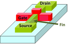
A Fin Field-effect transistor (FinFET) is a MOSFET built on a substrate where the gate is placed on two, three, or four sides of the channel or wrapped around the channel, forming a double gate structure. These devices have been given the generic name "finfets" because the source/drain region forms fins on the silicon surface. The FinFET devices have significantly faster switching times and higher current density than the mainstream CMOS technology.
The term FinFET (fin field-effect transistor) was coined in 2001 by University of California, Berkeley, researchers (Profs. Chenming Hu, Tsu-Jae King-Liu and Jeffrey Bokor) to describe a nonplanar, double-gate transistor built on an SOI substrate,[1] based on the earlier DELTA (single-gate) transistor design.[2][3][4]
The FinFET transistors can have gate thickness of 5 nanometres and gate width under 50 nm, are supposed to find application in sub-28 nanometer chips. FinFET technology is being pursued by AMD, NVidia[5], IBM, and Motorola and in academia.
The industry's first 25 nanometre transistor operating on just 0.7 volt was demonstrated in December 2002 by TSMC. The "Omega FinFET" design, named after the similarity between the Greek letter "Omega" and the shape in which the gate wraps around the source/drain structure, has a gate delay of just 0.39 picosecond (ps) for the N-type transistor and 0.88 ps for the P-type.
Intel's tri-gate transistors, where the gate surrounds the channel on three sides, allow for increased energy efficiency and lower gate delay—and thus greater performance—over planar transistors.[6][7]
The first finfet transistor type was known under the name of fully Depleted Lean-channel TrAnsistor or DELTA transistor. Articles covering the DELTA transistor were first published in the beginning of the 1990s. The gate of the transistor can cover and electrically contact the semiconductor channel fin on both the top and the sides or only on the sides. The former is called a tri-gate transistor and the latter a double-gate transistor. A double-gate transistor optionally can have each side connected to two different terminal or contacts. This variant is called split transistor. This enables more refined control of the operation of the transistor.
Reference
- ↑ Xuejue Huang; Wen-Chin Lee; Kuo, C.; et al. (May 2001). "Sub-50 nm P-channel FinFET" (PDF). IEEE Transactions on Electron Devices. 48 (5): 880–886. doi:10.1109/16.918235.
- ↑ Hisamoto, D.; Kaga, T.; Takeda, E. (June 1991). "Impact of the vertical SOI 'DELTA' structure on planar device technology" (PDF). IEEE Transactions on Electron Devices. 38 (6): 1419–1424. doi:10.1109/16.81634. Archived from the original (PDF) on 2016-12-01.
- ↑ Hisamoto, D. et al. (1991) "Impact of the vertical SOI 'Delta' Structure on Planar Device Technology" IEEE Trans. Electron. Dev. 41 p. 745.
- ↑ Chenming Hu; Bokor, J.; et al. (December 2000). "FinFET-a self-aligned double-gate MOSFET scalable to 20 nm". IEEE Transactions on Electron Devices. 47 (12): 2320–2325. doi:10.1109/16.887014.
- ↑ NVidia Pascal Microarchitecture
- ↑ Bohr, Mark; Mistry, Kaizad (May 2011). "Inte's Revolutionary 22 nm Transistor Technology" (PDF). intel.com. Retrieved April 18, 2018.
- ↑ Grabham, Dan (May 6, 2011). "Intel's Tri-Gate transistors: everything you need to know". TechRadar. Retrieved April 19, 2018.