Electronic design automation
Electronic design automation (EDA), also referred to as electronic computer-aided design (ECAD),[1] is a category of software tools for designing electronic systems such as integrated circuits and printed circuit boards. The tools work together in a design flow that chip designers use to design and analyze entire semiconductor chips. Since a modern semiconductor chip can have billions of components, EDA tools are essential for their design.
This article describes EDA specifically with respect to integrated circuits.
History
Early days
Before EDA, integrated circuits were designed by hand, and manually laid out. Some advanced shops used geometric software to generate the tapes for the Gerber photoplotter, but even those copied digital recordings of mechanically drawn components. The process was fundamentally graphic, with the translation from electronics to graphics done manually. The best known company from this era was Calma, whose GDSII format survives.
By the mid-1970s, developers started to automate the design along with the drafting. The first placement and routing (Place and route) tools were developed. The proceedings of the Design Automation Conference cover much of this era.
The next era began about the time of the publication of "Introduction to VLSI Systems" by Carver Mead and Lynn Conway in 1980. This ground breaking text advocated chip design with programming languages that compiled to silicon. The immediate result was a considerable increase in the complexity of the chips that could be designed, with improved access to design verification tools that used logic simulation. Often the chips were easier to lay out and more likely to function correctly, since their designs could be simulated more thoroughly prior to construction. Although the languages and tools have evolved, this general approach of specifying the desired behavior in a textual programming language and letting the tools derive the detailed physical design remains the basis of digital IC design today.
The earliest EDA tools were produced academically. One of the most famous was the "Berkeley VLSI Tools Tarball", a set of UNIX utilities used to design early VLSI systems. Still widely used are the Espresso heuristic logic minimizer and Magic.
Another crucial development was the formation of MOSIS, a consortium of universities and fabricators that developed an inexpensive way to train student chip designers by producing real integrated circuits. The basic concept was to use reliable, low-cost, relatively low-technology IC processes, and pack a large number of projects per wafer, with just a few copies of each projects' chips. Cooperating fabricators either donated the processed wafers, or sold them at cost, seeing the program as helpful to their own long-term growth.
Birth of commercial EDA
1981 marks the beginning of EDA as an industry. For many years, the larger electronic companies, such as Hewlett Packard, Tektronix, and Intel, had pursued EDA internally. In 1981, managers and developers spun out of these companies to concentrate on EDA as a business. Daisy Systems, Mentor Graphics, and Valid Logic Systems were all founded around this time, and collectively referred to as DMV. Within a few years there were many companies specializing in EDA, each with a slightly different emphasis. The first trade show for EDA was held at the Design Automation Conference in 1984.
In 1981, the U.S. Department of Defense began funding of VHDL as a hardware description language. In 1986, Verilog, another popular high-level design language, was first introduced as a hardware description language by Gateway Design Automation. Simulators quickly followed these introductions, permitting direct simulation of chip designs: executable specifications. In a few more years, back-ends were developed to perform logic synthesis.
Current status
Current digital flows are extremely modular (see Integrated circuit design, Design closure, and Design flow (EDA)). The front ends produce standardized design descriptions that compile into invocations of "cells,", without regard to the cell technology. Cells implement logic or other electronic functions using a particular integrated circuit technology. Fabricators generally provide libraries of components for their production processes, with simulation models that fit standard simulation tools. Analog EDA tools are far less modular, since many more functions are required, they interact more strongly, and the components are (in general) less ideal.
EDA for electronics has rapidly increased in importance with the continuous scaling of semiconductor technology.[2] Some users are foundry operators, who operate the semiconductor fabrication facilities, or "fabs", and design-service companies who use EDA software to evaluate an incoming design for manufacturing readiness. EDA tools are also used for programming design functionality into FPGAs.
Software focuses
Design
- High-level synthesis (or behavioural synthesis, algorithmic synthesis) – high-level design description (e.g. in C/C++) is converted into RTL.
- Logic synthesis – translation of RTL design description (e.g. written in Verilog or VHDL) into a discrete netlist of logic gates.
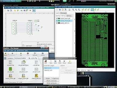
- Schematic capture – For standard cell digital, analog, RF-like Capture CIS in Orcad by Cadence and ISIS in Proteus
- Layout – usually schematic-driven layout, like Layout in Orcad by Cadence, ARES in Proteus
Simulation
- Transistor simulation – low-level transistor-simulation of a schematic/layout's behavior, accurate at device-level.
- Logic simulation – digital-simulation of an RTL or gate-netlist's digital (boolean 0/1) behavior, accurate at boolean-level.
- Behavioral Simulation – high-level simulation of a design's architectural operation, accurate at cycle-level or interface-level.
- Hardware emulation – Use of special purpose hardware to emulate the logic of a proposed design. Can sometimes be plugged into a system in place of a yet-to-be-built chip; this is called in-circuit emulation.
- Technology CAD simulate and analyze the underlying process technology. Electrical properties of devices are derived directly from device physics.
- Electromagnetic field solvers, or just field solvers, solve Maxwell's equations directly for cases of interest in IC and PCB design. They are known for being slower but more accurate than the layout extraction above.
Analysis and verification
- Functional verification
- Clock Domain Crossing Verification (CDC check): Similar to linting, but these checks/tools specialize in detecting and reporting potential issues like data loss, meta-stability due to use of multiple clock domains in the design.
- Formal verification, also model checking: Attempts to prove, by mathematical methods, that the system has certain desired properties, and that certain undesired effects (such as deadlock) cannot occur.
- Equivalence checking: algorithmic comparison between a chip's RTL-description and synthesized gate-netlist, to ensure functional equivalence at the logical level.
- Static timing analysis: Analysis of the timing of a circuit in an input-independent manner, hence finding a worst case over all possible inputs.
- Physical verification, PV: checking if a design is physically manufacturable, and that the resulting chips will not have any function-preventing physical defects, and will meet original specifications.
Manufacturing preparation
- Mask data preparation, MDP: generation of actual lithography photomask used to physically manufacture the chip.
- Resolution enhancement techniques, RET – methods of increasing of quality of final photomask.
- Optical proximity correction, OPC – up-front compensation for diffraction and interference effects occurring later when chip is manufactured using this mask.
- Mask generation – generation of flat mask image from hierarchical design.
- Automatic test pattern generation, ATPG – generates pattern-data to systematically exercise as many logic-gates, and other components, as possible.
- Built-in self-test, or BIST – installs self-contained test-controllers to automatically test a logic (or memory) structure in the design
Functional Safety
- Functional Safety Analysis, Systematic computation of failure in time (FIT) rates and diagnostic coverage metrics for designs in order to meet the compliance requirements for the desired safety integrity levels.
- Functional Safety Synthesis, Add reliability enhancements to structured elements (Modules, RAMs, ROMs, Register Files, FIFOs) to improves fault detection / fault tolerance. These includes (not limited to), Addition of error detection and / or correction codes (Hamming), Redundant logic for fault detection and fault tolerance (duplicate / triplicate) and Protocol checks (Interface parity, address alignment, beat count)
- Functional Safety Verification,Running of a fault campaign, including insertion of faults into the design and verification that the safety mechanism reacts in an appropriate manner for the faults that are deemed covered.
Companies
Old companies
Market capitalization and company name as of December 2011:[3]
- $5.77 billion[4] – Synopsys
- $4.46 billion[5] – Cadence
- $2.33 billion – Mentor Graphics
- $507 million – Magma Design Automation; Synopsys acquired Magma in February 2012[6][7]
- NT$6.44 billion – SpringSoft; Synopsys acquired SpringSoft in August 2012
- ¥11.95 billion – Zuken Inc.
Note: EEsof should likely be on this list,[8] but it does not have a market cap as it is the EDA division of Keysight.
Acquisitions
Many of the EDA companies acquire small companies with software or other technology that can be adapted to their core business.[9] Most of the market leaders are amalgamations of many smaller companies.[10] This trend is helped by the tendency of software companies to design tools as accessories that fit naturally into a larger vendor's suite of programs on digital circuitry, many new tools incorporate analog design, and mixed systems. This is happening because there is now a trend to place entire electronic systems on a single chip.
See also
| Wikimedia Commons has media related to Electronic design automation. |
References
- ↑ "About the EDA Industry". Electronic Design Automation Consortium. Archived from the original on August 2, 2015. Retrieved July 29, 2015.
- ↑ Lavagno, Martin, and Scheffer (2006). Electronic Design Automation For Integrated Circuits Handbook. Taylor and Francis. ISBN 0849330963.
- ↑ Company Comparison - Google Finance. Google.com. Retrieved on 2013-08-10.
- ↑ Synopsys, Inc.: NASDAQ:SNPS quotes & news - Google Finance. Google.com (2013-05-22). Retrieved on 2013-08-10.
- ↑ CDNS Key Statistics | Cadence Design Systems, Inc. Stock - Yahoo! Finance. Finance.yahoo.com. Retrieved on 2013-08-10.
- ↑ Dylan McGrath (30 Nov 2011). "Synopsys to buy Magma for $507 million". EETimes.
- ↑ "Synopsys to Acquire Magma Design Automation".
- ↑ "Agilent EEsof EDA – Part I".
- ↑ Kirti Sikri Desai (2006). "EDA Innovation through Merger and Acquisitions". EDA Cafe. Retrieved March 23, 2010.
- ↑ List of EDA mergers and acquisitions at SemiWiki.com
- Notes
- http://www.staticfreesoft.com/documentsTextbook.html Computer Aids for VLSI Design by Steven M. Rubin
- Electronic Design Automation For Integrated Circuits Handbook, by Lavagno, Martin, and Scheffer, ISBN 0-8493-3096-3, 2006
- Combinatorial Algorithms for Integrated Circuit Layout, by Thomas Lengauer, ISBN 3-519-02110-2, Teubner Verlag, 1997.
- The Electronic Design Automation Handbook, by Dirk Jansen et al., Kluwer Academic Publishers, ISBN 1-4020-7502-2, 2003, available also in German ISBN 3-446-21288-4 (2005)