EEPROM
| Computer memory types |
|---|
| Volatile |
| RAM |
| Historical |
|
| Non-volatile |
| ROM |
| NVRAM |
| Early stage NVRAM |
| Magnetic |
| Optical |
| In development |
| Historical |
|
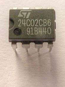


EEPROM (also E2PROM) stands for Electrically Erasable Programmable Read-Only Memory and is a type of non-volatile memory used in computers, integrated in microcontrollers for smart cards and remote keyless system, and other electronic devices to store relatively small amounts of data but allowing individual bytes to be erased and reprogrammed.
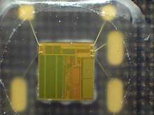
EEPROMs are organized as arrays of floating-gate transistors. EEPROMs can be programmed and erased in-circuit, by applying special programming signals. Originally, EEPROMs were limited to single byte operations which made them slower, but modern EEPROMs allow multi-byte page operations. It also has a limited life for erasing and reprogramming, now reaching a million operations in modern EEPROMs. In an EEPROM that is frequently reprogrammed while the computer is in use, the life of the EEPROM is an important design consideration.
Flash memory is a type of EEPROM designed for high speed and high density, at the expense of large erase blocks (typically 512 bytes or larger) and limited number of write cycles (often 10,000). There is no clear boundary dividing the two, but the term "EEPROM" is generally used to describe non-volatile memory with small erase blocks (as small as one byte) and a long lifetime (typically 1,000,000 cycles). Many microcontrollers include both: flash memory for the firmware, and a small EEPROM for parameters and history.
History
In early 1970s, some studies, inventions, and development for electrically re-programmable non-volatile memories were performed by various companies and organizations. Especially, in 1971, the earliest research report was presented at the 3rd Conference on Solid State Devices, Tokyo in Japan by Yasuo Tarui, Yutaka Hayashi, and Kiyoko Nagai at Electrotechnical Laboratory; a Japanese national research institute.[1] They continued this study for more than 10 years.[2][3] These papers have been repeatedly cited by later papers and patents.[4][5]
One of their research includes MONOS (metal-oxide-nitride-oxide-semiconductor) technology,[6] which is utilized Renesas Electronics' flash memory integrated in single-chip microcontrollers until today.[7][8][9]
In 1972, one of electrically re-programmable non-volatile memory was invented by Fujio Masuoka at Toshiba, who is also known as the inventor of flash memory.[10] Most of major semiconductor manufactures, such as Toshiba,[10][4] Sanyo (later, ON Semiconductor),[11] IBM,[12] Intel,[13][14] NEC (later, Renesas Electronics),[15] Philips (later, NXP Semiconductors),[16] Siemens (later, Infineon Technologies),[17] Honeywell (later, Atmel),[18] Texas Instruments,[19] studied, invented, and manufactured some electrically re-programmable non-volatile devices until 1977.
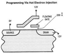
The theoretical basis of these devices is Avalanche hot-carrier injection. But in general, programmable memories, including EPROM, of early 1970s had reliability problems such as the data retention periods and the number of erase/write cycle endurance.[20]
In 1975, NEC's semiconductor operations unit, later NEC Electronics, currently Renesas Electronics, applied the trademark name EEPROM® to Japan Patent Office.[21][22] In 1978, this trademark right is granted and registered as No.1,342,184 in Japan, and still survives as of March 2018.
In February 1977, Eliyahou Harari at Hughes Aircraft Company invented a new EEPROM technology utilizing Fowler-Nordheim tunnelling through a thin silicon dioxide layer between the floating-gate and the substrate. Hughes went on to produce this new EEPROM devices.[23] But this patent[24] cited NEC's EEPROM® invention.[15]
In May 1977, some important research result was disclosed by Fairchild and Siemens. They utilized SONOS (polysilicon-oxynitride-nitride-oxide-silicon) structure with thickness of silicon dioxide less than 30 Å, and SIMOS (stacked-gate injection MOS) structure, respectively, for utilizing Fowler-Nordheim tunnelling hot-carrier injection.[25][26]
Around 1976 to 1978, Intel's team, including George Perlegos, made some inventions to improve this tunneling E2PROM technology.[27][28] In 1978, they developed a 16K (2K word × 8) bit Intel 2816 device with a thin silicon dioxide layer, which was less than 200 Å.[29] In 1980. this structure was publicly introduced as FLOTOX; floating gate tunnel oxide.[30] The FLOTOX structure improved reliability of erase/write cycles per byte up to 10,000 times.[31] But this device required additional 20–22V VPP bias voltage supply for byte erase, except for 5V read operations.[32]:5-86 In 1981, Perlegos and 2 other members left Intel to form Seeq Technology,[33] which used on-device charge pumps to supply the high voltages necessary for programming E2PROMs. In 1984, Perlogos left Seeq Technology to found Atmel, then Seeq Technology was acquired by Atmel.[34][35]
Theoretical basis of FLOTOX structure
As is described in former section, old EEPROMs are based on Avalanche breakdown-based hot-carrier injection with high reverse breakdown voltage. But FLOTOX's theoretical basis is Fowler–Nordheim tunneling hot-carrier injection through a thin silicon dioxide layer between the floating-gate and the substrate. In other words, it uses tunnel junction mechanism.[36]
Theoretical basis of the physical phenomenon itself is the same as today's flash memory. But each FLOTOX structure is in conjunction with another read-control transistor because the floating gate itself is just programming and erasing one data bit.[37]
Intel's FLOTOX device structure improved EEPROM's reliability, in other words, the write and erase cycles endurance, and the data retention period. A material of study for single event effect about FLOTOX is available.[38]
Today, detailed academical explanation of FLOTOX device structure can be found in various materials.[39][40][41]
Today's EEPROM structure
Nowadays, EEPROM is used for embedded microcontrollers as well as standard EEPROM products. EEPROM still requires 2 transistors structure per bit to erase a dedicated byte in the memory, while flash memory has 1 transistor per bit to erase a region of the memory.[42]:245, PDF:2
Security protections
Because EEPROM technology is used for some security gadgets, such as credit card, SIM card, key-less entry, etc., some devices have security protection mechanisms.[42][43]
Electrical interface
EEPROM devices use a serial or parallel interface for data input/output.
Serial bus devices
The common serial interfaces are SPI, I²C, Microwire, UNI/O, and 1-Wire. These use from 1 to 4 device pins and allow devices to use packages with 8-pins or less.
A typical EEPROM serial protocol consists of three phases: OP-Code Phase, Address Phase and Data Phase. The OP-Code is usually the first 8-bits input to the serial input pin of the EEPROM device (or with most I²C devices, is implicit); followed by 8 to 24 bits of addressing depending on the depth of the device, then the read or write data.
Each EEPROM device typically has its own set of OP-Code instructions mapped to different functions. Common operations on SPI EEPROM devices are:
- Write Enable (WRENAL)
- Write Disable (WRDI)
- Read Status Register (RDSR)
- Write Status Register (WRSR)
- Read Data (READ)
- Write Data (WRITE)
Other operations supported by some EEPROM devices are:
- Program
- Sector Erase
- Chip Erase commands
Parallel bus devices
Parallel EEPROM devices typically have an 8-bit data bus and an address bus wide enough to cover the complete memory. Most devices have chip select and write protect pins. Some microcontrollers also have integrated parallel EEPROM.
Operation of a parallel EEPROM is simple and fast when compared to serial EEPROM, but these devices are larger due to the higher pin count (28 pins or more) and have been decreasing in popularity in favor of serial EEPROM or flash.
Other devices
EEPROM memory is used to enable features in other types of products that are not strictly memory products. Products such as real-time clocks, digital potentiometers, digital temperature sensors, among others, may have small amounts of EEPROM to store calibration information or other data that needs to be available in the event of power loss. It was also used on video game cartridges to save game progress and configurations, before the usage of external and internal flash memories.
Failure modes
There are two limitations of stored information; endurance, and data retention.
During rewrites, the gate oxide in the floating-gate transistors gradually accumulates trapped electrons. The electric field of the trapped electrons adds to the electrons in the floating gate, lowering the window between threshold voltages for zeros vs ones. After sufficient number of rewrite cycles, the difference becomes too small to be recognizable, the cell is stuck in programmed state, and endurance failure occurs. The manufacturers usually specify the maximum number of rewrites being 1 million or more.[44]
During storage, the electrons injected into the floating gate may drift through the insulator, especially at increased temperature, and cause charge loss, reverting the cell into erased state. The manufacturers usually guarantee data retention of 10 years or more.[45]
Related types
Flash memory is a later form of EEPROM. In the industry, there is a convention to reserve the term EEPROM to byte-wise erasable memories compared to block-wise erasable flash memories. EEPROM occupies more die area than flash memory for the same capacity, because each cell usually needs a read, a write, and an erase transistor, while flash memory erase circuits are shared by large blocks of cells (often 512×8).
Newer non-volatile memory technologies such as FeRAM and MRAM are slowly replacing EEPROMs in some applications, but are expected to remain a small fraction of the EEPROM market for the foreseeable future.
Comparison with EPROM and EEPROM/flash
The difference between EPROM and EEPROM lies in the way that the memory programs and erases. EEPROM can be programmed and erased electrically using field electron emission (more commonly known in the industry as "Fowler–Nordheim tunneling").
EPROMs can't be erased electrically and are programmed via hot carrier injection onto the floating gate. Erase is via an ultraviolet light source, although in practice many EPROMs are encapsulated in plastic that is opaque to UV light, making them "one-time programmable".
Most NOR flash memory is a hybrid style—programming is through hot carrier injection and erase is through Fowler–Nordheim tunneling.
| Type | Inject electrons onto gate (mostly interpreted as Bit=0) |
Duration | Remove electrons from gate (mostly interpreted as Bit=1) |
Duration/Mode |
|---|---|---|---|---|
| EEPROM | field electron emission | 0,1 ... 5 ms, bytewise | field electron emission | 0,1 ... 5 ms, blockwise |
| NOR Flash memory | hot carrier injection | 0,01 ... 1 ms | field electron emission | 0,01 ... 1 ms, blockwise |
| EPROM | hot carrier injection | 3 ... 50 ms, bytewise | UV light | 5 ... 30 minutes, whole chip |
EEPROM manufacturers
- Atmel, later Microchip Technology
- Hitachi, later Renesas Technology, then Renesas Electronics
- Infineon
- Intersil, later Renesas Electronics
- Linear Technology, later Analog Devices
- Macronix
- Maxwell Technologies
- Microchip Technology
- Mitsubishi Electric, later Renesas Technology, then Renesas Electronics
- NEC Corporation, later NEC Electronics, then Renesas Electronics
- NXP Semiconductors
- National Semiconductor (no longer makes standalone EEproms) later, Texas Instruments
- ON Semiconductor
- Renesas Electronics
- ROHM
- Samsung Electronics
- STMicroelectronics
- Seiko Instruments
- Winbond
In popular culture
The Stanford Graduate Students in Electrical Engineering (GSEE) has annually hosted a dance (i.e. prom) called EEPROM[46] since 2012.
See also
References
- ↑ Tarui, Yasuo; Hayashi, Yutaka; Nagai, Kiyoko (1971-09-01). "Proposal of electrically reprogrammable non-volatile semiconductor memory". Proceedings of the 3rd Conference on Solid State Devices, Tokyo. The Japan Society of Applied Physics: 155–162.
- ↑ Tarui, Y.; Hayashi, Y.; Nagai, K. (1972). "Electrically reprogrammable nonvolatile semiconductor memory". IEEE Journal of Solid-State Circuits. 7 (5): 369–375. Bibcode:1972IJSSC...7..369T. doi:10.1109/JSSC.1972.1052895. ISSN 0018-9200. Archived from the original on 2018-03-09.
- ↑ Tarui, Yasuo; Nagai, Kiyoko; Hayashi, Yutaka (1974-07-19). "Nonvolatile Semiconductor Memory" (PDF). OYOBUTURI. 43 (10): 990–1002. doi:10.11470/oubutsu1932.43.990. ISSN 2188-2290. Archived (PDF) from the original on 2018-03-12.
- 1 2 Iizuka, H.; Masuoka, F.; Sato, Tai; Ishikawa, M. (1976). "Electrically alterable avalanche-injection-type MOS READ-ONLY memory with stacked-gate structure". IEEE Transactions on Electron Devices. 23 (4): 379–387. Bibcode:1976ITED...23..379I. doi:10.1109/T-ED.1976.18415. ISSN 0018-9383. Archived from the original on 2018-03-12.
- ↑ Rossler, B. (1977). "Electrically erasable and reprogrammable read-only memory using the n-channel SIMOS one-transistor cell". IEEE Transactions on Electron Devices. 24 (5): 606–610. Bibcode:1977ITED...24..606R. doi:10.1109/T-ED.1977.18788. ISSN 0018-9383. Archived from the original on 2018-05-03.
- ↑ Suzuki, E.; Hiraishi, H.; Ishii, K.; Hayashi, Y. (1983). "A low-voltage alterable EEPROM with metal—oxide-nitride—oxide—semiconductor (MONOS) structures". IEEE Transactions on Electron Devices. 30 (2): 122–128. Bibcode:1983ITED...30..122S. doi:10.1109/T-ED.1983.21085. ISSN 0018-9383. Archived from the original on 2018-03-12.
- ↑ XTECH, NIKKEI. "Renesas Embeds 40nm Flash Memory on Chip". NIKKEI XTECH. Archived from the original on 2018-03-13.
- ↑ "Renesas Electronics Develops 90 nm One-Transistor MONOS Flash Memory Technology to Accelerate Intelligence in Automotive Control Systems". Business Wire. 2016-01-03. Archived from the original on 2018-03-13.
- ↑ Taito, Y.; Kono, T.; Nakano, M.; Saito, T.; Ito, T.; Noguchi, K.; Hidaka, H.; Yamauchi, T. (2015). "A 28 nm Embedded Split-Gate MONOS (SG-MONOS) Flash Macro for Automotive Achieving 6.4 GB/s Read Throughput by 200 MHz No-Wait Read Operation and 2.0 MB/s Write Throughput at Tj of 170circ$ C". IEEE Journal of Solid-State Circuits. 51 (1): 213–221. Bibcode:2016IJSSC..51..213.. doi:10.1109/JSSC.2015.2467186. ISSN 0018-9200. Archived from the original on 2018-05-03.
- 1 2 Masuoka, Fujio (31 August 1972). "Avalanche injection type mos memory".
- ↑ Rai, Yasuki; Sasami, Terutoshi; Hasegawa, Yuzuru; Okazoe, Masaru (1973-05-18). "Electrically reprogrammable nonvolatile floating gate semi-conductor memory device and method of operation". Archived from the original on 2018-05-03.
- ↑ Abbas, Shakir A.; Barile, Conrad A.; Lane, Ralph D.; Liu., Peter T (1973-03-16). "US3836992A; Electrically erasable floating gate fet memory cell". pdfpiw.uspto.gov. United States Patent and Trademark Office. Archived from the original on 2018-03-09.
- ↑ Frohman, Bentchkowsky D (19 October 1973). "Electrically alterable floating gate device and method for altering same".
- ↑ Chou, Sunlin (26 February 1973). "Erasable floating gate device".
- 1 2 Ohya, Shuichi; Kikuchi, Masanori (1974-12-27). "Non-volatile semiconductor memory device".
- ↑ Verwey, J. F.; Kramer, R. P. (1974). "Atmos—An electrically reprogrammable read-only memory device". IEEE Transactions on Electron Devices. 21 (10): 631–636. Bibcode:1974ITED...21..631V. doi:10.1109/T-ED.1974.17981. ISSN 0018-9383. Archived from the original on 2018-03-10.
- ↑ B., Roessler; R. G., Mueller (1975). "Erasable and electrically reprogrammable read-only memory using the N-channel SIMOS one-transistor cell". Siemens Forschungs und Entwicklungsberichte. 4: 345–351. Bibcode:1975SiFoE...4..345R.
- ↑ Jack, S; Huang, T. (8 September 1975). "Semiconductor memory cell".
- ↑ Gosney, W. M. (1977). "DIFMOS—A floating-gate electrically erasable nonvolatile semiconductor memory technology". IEEE Transactions on Electron Devices. 24 (5): 594–599. Bibcode:1977ITED...24..594G. doi:10.1109/T-ED.1977.18786. ISSN 0018-9383. Archived from the original on 2018-03-12.
- ↑ Moskowitz, Sanford L. (2016). "reliability%20problems"+EPROM+1970s Advanced Materials Innovation: Managing Global Technology in the 21st century. John Wiley & Sons. ISBN 9781118986097.
- ↑ "EEPROM". TMview. Archived from the original on 2018-03-10.
- ↑ "Reg. No.1342184 – LIVE – REGISTRATION – Issued and Active".
- ↑ "Archived copy" (PDF). Archived (PDF) from the original on 2015-02-07. Retrieved 2015-02-05.
- ↑ Harari, Eliyahou (22 February 1977). "Electrically erasable non-volatile semiconductor memory". Archived from the original on 3 May 2018.
- ↑ Chen, P. C. Y. (May 1977). "Threshold-alterable Si-gate MOS devices". IEEE Transactions on Electron Devices. 24 (5): 584–586. Bibcode:1977ITED...24..584C. doi:10.1109/T-ED.1977.18783. ISSN 0018-9383. Archived from the original on 2018-03-12.
- ↑ Rossler, B. (May 1977). "Electrically erasable and reprogrammable read-only memory using the n-channel SIMOS one-transistor cell". IEEE Transactions on Electron Devices. 24 (5): 606–610. Bibcode:1977ITED...24..606R. doi:10.1109/T-ED.1977.18788. ISSN 0018-9383. Archived from the original on 2018-05-03.
- ↑ Simko, Richard T. (17 March 1977). "Electrically programmable and electrically erasable MOS memory cell".
- ↑ Frohman-Bentchkowsky, Dov; Mar, Jerry; Perlegos, George; Johnson, William S. (15 December 1978). "Electrically programmable and erasable MOS floating gate memory device employing tunneling and method of fabricating same".
- ↑ Dummer, G. W. A. (2013). Electronic Inventions and Discoveries: Electronics from Its Earliest Beginnings to the Present Day. Elsevier. ISBN 9781483145211.
- ↑ Johnson, W.; Perlegos, G.; Renninger, A.; Kuhn, G.; Ranganath, T. (1980). "A 16Kb electrically erasable nonvolatile memory". 1980 IEEE International Solid-State Circuits Conference. Digest of Technical Papers. XXIII: 152–153. doi:10.1109/ISSCC.1980.1156030. Archived from the original on 2018-03-13.
- ↑
Euzent, B.; Boruta, N.; Lee, J.; Jenq, C. (1981). "Reliability Aspects of a Floating Gate E2 PROM". 19th International Reliability Physics Symposium: 11–16. doi:10.1109/IRPS.1981.362965. Archived from the original on 2018-03-13.
The Intel 2816 uses the FLOTOX structure, which has been discussed in detail in the literaturel. Basically, it utilizes an oxide of less than 200A thick between the floating polysilicon gate and the N+ region as shown in Figure 1. - ↑ 2816A-2 PDF Datasheet - Intel Corporation - Datasheets360.com. Intel. October 1983.
- ↑ "Seeq Technology » AntiqueTech". Archived from the original on 2014-10-02.
- ↑ Rostky, George (July 2, 2002). "Remembering the PROM knights of Intel". EE Times. Archived from the original on September 29, 2007. Retrieved 2007-02-08.
- ↑ Atmel AT28C16 datasheet (PDF) (0540B ed.). October 1998. Archived (PDF) from the original on 2017-08-29.
- ↑ Gutmann, Peter (2001-08-15). "Data Remanence in Semiconductor Devices". 10th USENIX SECURITY SYMPOSIUM. IBM T.J.Watson Research Center: 39–54. Archived from the original on 2016-10-12.
- ↑ Janwadkar, Sudhanshu (2017-10-24). "Fabrication of Floating Gate MOS (FLOTOX)". www.slideshare.net.
- ↑ Koga, R.; Tran, V.; George, J.; Crawford, K.; Crain, S.; Zakrzewski, M.; Yu, P. "SEE Sensitivities of Selected Advanced Flash and First-In-First-Out Memories" (PDF). The Aerospace Corporation. Archived (PDF) from the original on 2018-03-14.
- ↑ Fuller, Dr. Lynn (2012-02-22). CMOS Process Variations EEPROM Fabrication Technology. Microelectronic Engineering, Rochester Institute of Technology.
- ↑ Groeseneken, G.; Maes, H.E.; VanHoudt, J.; Witters, J.S. Basics of Nonvolatile Semiconductor Memory Devices. Archived from the original on 2015-10-27.
- ↑ Bergemont, Albert; Chi, Min-Hwa (1997-05-05). "US Patent 5856222: Method of fabricating a high density EEPROM cell". patents.google.com. National Semiconductor Corp.
- 1 2 Skorobogatov, Sergei (2017). How Microprobing Can Attack Encrypted Memory (PDF). 2017 Euromicro Conference on Digital System Design (DSD). Vienna. pp. 244–251. doi:10.1109/DSD.2017.69. ISBN 978-1-5386-2146-2.
- ↑ "Breaking copy protection in microcontrollers". www.cl.cam.ac.uk. Archived from the original on 2017-10-22.
- ↑ "Frequently Asked Questions -ROHM Semiconductor". Archived from the original on 2011-02-19.
- ↑ System Integration - From Transistor Design to Large Scale Integrated Circuits
- ↑ "Stanford Graduate Students in Electrical Engineering (GSEE) - Facebook". Archived from the original on 2017-12-07.