Solaristor

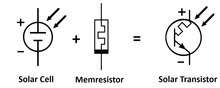
A solaristor (from SOLAR cell transISTOR) is a compact two terminal self-powered phototransistor. The two-in-one transistor plus solar cell achieves the high-low current modulation by a memresistive effect in the flow of photogenerated carriers. The term was coined by Dr Amador Perez-Tomas working in collaboration with other ICN2 researchers in 2018 when they demonstrated the concept in a ferroelectric-oxide/organic bulk heterojunction solar cell.[1]
Principle of operation
In a basic Solaristor embodiment, the self-powered transistor effect is achieved by the integration of a light absorber layer (a material that absorbs photon energy) in series with a functional semiconductor transport layer, which internal conductivity or contact resistance can be modified externally.
The Light Absorber (The Solar Cell element)
In general, the light absorber is a semiconductor p-n junction that:
- Efficiently harvests photons at different visible wavelengths by the photoelectric effect.
- Splits photo-generated excitons into free electron and holes.
- Bring these free electrons and holes towards their respective outer electrodes by means of an internal field.
Additionally, in thin-film solar cells, buffer electron and hole semiconductor transport layers are introduced at the respective metal electrodes to avoid electron-hole recombination and to remove the metal/absorber Schottky barrier.
The Conductivity Modulation (The Transistor element)
A Solaristor effect is achieved by modifying the internal field properties or the overall conductivity of the solar cell.
Ferroelectric Solaristors. One possibility is the use of ferroelectric semiconductors as transport layers. A ferroelectric layer can be seen as a semiconductor with switchable surface charge polarity. Because of this tuneable dipole effect, ferroelectrics bend their electronic band structure and offsets with respect to adjacent metals and/or semiconductors when switching the ferroelectric polarization so that the overall conductivity can be tuned orders of magnitude.
Two Terminal Phototransistors
Conventional photodiodes or photodetectors do not switch as a phototransistor does when biased through its third terminal (gate). An additional advantage of a Solaristor is, therefore, the potential reduction of the standard phototransistor’s area and interconnection complexity. By using Solaristors, it would be possible in theory to replace the in-plane three-electrode architecture by a vertical, two-electrode photodiode-like architecture in systems like photo-sensors, cameras or displays.
See also
References
- ↑ Pérez-Tomás, Amador; Lima, Anderson; Billon, Quentin; Shirley, Ian; Catalan, Gustau; Lira-Cantú, Mónica. "A Solar Transistor and Photoferroelectric Memory". Advanced Functional Materials. doi:10.1002/adfm.201707099. ISSN 1616-3028.