Charge pump


A charge pump is a kind of DC to DC converter that uses capacitors for energetic charge storage to raise or lower voltage. Charge-pump circuits are capable of high efficiencies, sometimes as high as 90–95%, while being electrically simple circuits.
Description
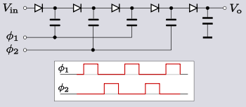
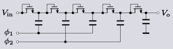
Charge pumps use some form of switching device to control the connection of a supply voltage across a load through a capacitor. In a two stage cycle, in the first stage a capacitor is connected across the supply, charging it to that same voltage. In the second stage the circuit is reconfigured so that the capacitor is in series with the supply and the load. This doubles the voltage across the load - the sum of the original supply and the capacitor voltages. The pulsing nature of the higher voltage switched output is often smoothed by the use of an output capacitor.
An external or secondary circuit drives the switching, typically at tens of kilohertz up to several megahertz. The high frequency minimizes the amount of capacitance required, as less charge needs to be stored and dumped in a shorter cycle.
Charge pumps can double voltages, triple voltages, halve voltages, invert voltages, fractionally multiply or scale voltages (such as ×3/2, ×4/3, ×2/3, etc.) and generate arbitrary voltages by quickly alternating between modes, depending on the controller and circuit topology.
They are commonly used in low-power electronics (such as mobile phones) to raise and lower voltages for different parts of the circuitry - minimizing power consumption by controlling supply voltages carefully.
Terminology for PLL
The term charge pump is also commonly used in phase-locked loop (PLL) circuits even though there is no pumping action involved unlike in the circuit discussed above. A PLL charge pump is merely a bipolar switched current source. This means that it can output positive and negative current pulses into the loop filter of the PLL. It cannot produce higher or lower voltages than its power and ground supply levels.
Applications
- A common application for charge-pump circuits is in RS-232 level shifters, where they are used to derive positive and negative voltages (often +10 V and −10 V) from a single 5 V or 3 V power supply rail.
- Charge pumps can also be used as LCD or white-LED drivers, generating high bias voltages from a single low-voltage supply, such as a battery.
- Charge pumps are extensively used in NMOS memories and microprocessors to generate a negative voltage "VBB" (about −3 V), which is connected to the substrate. This guarantees that all N+-to-substrate junctions are reversely biased by 3 V or more, decreasing junction capacitance and increasing circuit speed.[1]
- A charge pump providing a negative voltage spike has been used in NES-compatible games not licensed by Nintendo in order to stun the Nintendo Entertainment System lockout chip.[2]
- As of 2007, charge pumps are integrated into nearly all EEPROM and flash-memory integrated circuits. These devices require a high-voltage pulse to "clean out" any existing data in a particular memory cell before it can be written with a new value. Early EEPROM and flash-memory devices required two power supplies: +5 V (for reading) and +12 V (for erasing). As of 2007, commercially available flash memory and EEPROM memory requires only one external power supply – generally 1.8 V or 3.3 V. A higher voltage, used to erase cells, is generated internally by an on-chip charge pump.
- Charge pumps are used in H bridges in high-side drivers for gate-driving high-side n-channel power MOSFETs and IGBTs. When the centre of a half bridge goes low, the capacitor is charged through a diode, and this charge is used to later drive the gate of the high-side FET a few volts above the source voltage so as to switch it on. This strategy works well, provided the bridge is regularly switched and avoids the complexity of having to run a separate power supply and permits the more efficient n-channel devices to be used for both switches. This circuit (requiring the periodic switching of the high-side FET) may also be called a "bootstrap" circuit, and some would differentiate between that and a charge pump (which would not require that switching).
See also
References
- ↑ Jenne, F. "Substrate Bias Circuit", US Patent 3794862A, Feb 26, 1974.
- ↑ Kevin Horton. Colordreams Revision C. Last modified 2007-09-30. Accessed 2011-09-15.
Applying the equivalent resistor concept to calculating the power losses in the charge pumps
- J. C. Maxwell, A Treatise on Electricity and Magnetism, Oxford, The Clarendon Press, 1873, pp. 420–425, “Intermittent current,” Art. 775, 776.
- Z. Singer, A. Emanuel, and M. S. Erlicki, “Power regulation by means of a switched capacitor,” in Proc. of the Institution of Electrical Engineers, Vol. 119, №2, 1972, pp. 149–152.
- G. van Steenwijk, K. Hoen, and H. Wallinga, “Analysis and design of a charge pump circuit for high output current applications”, in Proc. 19th European Solid-State Circuits Conference (ESSCIRC) 1993, pp. 118–121.
- J. W. Kimball, P. T. Krein, and K. R. Cahill, “Modeling of capacitor impedance in switching converters,” IEEE Power Electronics Letters, Vol. 3, №4, 2005, pp. 136–140.
- K. Itoh, M. Horiguchi, and H. Tanaka, Ultra-Low Voltage Nano-Scale Memories, Series on Integrated Circuits and Systems, Springer, 2007, 400p.
- M. D. Seeman and S. R. Sanders, “Analysis and optimization of switched capacitor DC-DC Converters,” IEEE Transactions on Power Electronics, Vol. 23, №2, 2008, pp. 841–851.
- S. Ben-Yaakov and M. Evzelman, “Generic and unified model of switched capacitor converters,” IEEE Energy Conversion Congress and Expo. (ECCE) 2009, pp. 3501–3508.
- S. Ben-Yaakov, "On the influence of switch resistances on switched capacitor converters losses," IEEE Transactions on Industrial Electronics, 2011.
Charge pumps where the voltages across the capacitors follow the binary number system
- F. Ueno, T. Inoue, and I. Oota, “Realization of a new switched-capacitor transformer with a step-up transformer ratio 2n–1 using n capacitors,” IEEE International Symposium on Circuits and Systems (ISCAS) 1986, pp. 805–808.
- J. A. Starzyk, Y.-W. Jan, and F. Qiu, “A DC-DC charge pump design based on voltage doublers,” IEEE Transactions on Circuits and Systems, Part I, Vol. 48, №3, 2001, pp. 350–359.
- F. L. Luo, and H. Ye, “Positive output multiple-lift push–pull switched-capacitor Luo-converters,” IEEE Transactions on Industrial Electronics, Vol. 51, №3, 2004, pp. 594–602.
- S. Ben-Yaakov and A. Kushnerov, “Algebraic foundation of self-adjusting switched capacitors converters,” IEEE Energy Conversion Congress and Expo. (ECCE) 2009, pp. 1582–1589.
External links
- Charge Pump, inductorless, Voltage Regulators
- On-chip High-Voltage Generator Design
- Charge Pump DC/DC Converters. Applications, circuits and solutions using inductorless (charge pump) dc/dc converters.
- DC/DC Conversion without Inductors. General description of charge pump operation; example applications using Maxim controllers.
- Charge-Pump and Step-Up DC-DC Converter Solutions for Powering White LEDs in Series or Parallel Connections
- Circuit Board Layout Guidelines for White LED Charge Pumps
- Linearized three state phase detector by Steven F. Gillig (patent filed 1990, awarded 1990, assigned to Motorola)
- Linearized digital phase and frequency detector by John D. Hatchett and Andrew S. Olesin (patent filed 1980, awarded 1983, assigned to Motorola)
- Charge pump circuits overview. Tutorial by G. Palumbo and D. Pappalardo