Integrated circuits are put into protective packages to allow easy handling and assembly onto printed circuit boards and to protect the devices from damage. A very large number of different types of package exist. Some package types have standardized dimensions and tolerances, and are registered with trade industry associations such as JEDEC and Pro Electron. Other types are proprietary designations that may be made by only one or two manufacturers. Integrated circuit packaging is the last assembly process before testing and shipping devices to customers.
Occasionally specially-processed integrated circuit dies are prepared for direct connections to a substrate without an intermediate header or carrier. In flip chip systems the IC is connected by solder bumps to a substrate. In beam-lead technology, the metallized pads that would be used for wire bonding connections in a conventional chip are thickened and extended to allow external connections to the circuit. Assemblies using "bare" chips have additional packaging or filling with epoxy to protect the devices from moisture.
Through-hole packages
Through-hole technology uses holes drilled through the PCB for mounting the components. The component has leads that are soldered to pads on the PCB to electrically and mechanically connect them to the PCB.
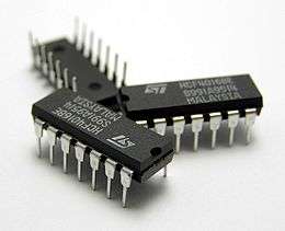
Three 14-pin (DIP14) plastic dual in-line packages containing IC chips.
| Acronym | Full name | Remark |
| SIP | Single in-line package | |
| DIP | Dual in-line package | 0.1 in (2.54 mm) pin spacing, rows 0.3 in (7.62 mm) or 0.6 in (15.24 mm) apart. |
| CDIP | Ceramic DIP[1] | |
| CERDIP | Glass-sealed ceramic DIP[1] | |
| QIP | Quadruple in-line package | Like DIP but with staggered (zig-zag) pins.[1] |
| SDIP | Skinny DIP | Standard DIP with 0.1 in (2.54 mm) pin spacing, rows 0.3 in (7.62 mm) apart.[1] |
| SDIP | Shrink DIP | Non-standard DIP with smaller 0.07 in (1.78 mm) pin spacing.[1] |
| ZIP | Zig-zag in-line package | |
| MDIP | Molded DIP[2] | |
| PDIP | Plastic DIP[1] | |
Surface mount
| Acronym | Full name | Remark |
| CCGA | Ceramic column-grid array (CGA)[3] | |
| CGA | Column-grid array[3] | Example |
| CERPACK | Ceramic package[4] | |
| CQGP[5] | | |
| LLP | Lead-less lead-frame package | A package with metric pin distribution (0.5–0.8 mm pitch)[6] |
| LGA | Land grid array[3] | |
| LTCC | Low-temperature co-fired ceramic[7] | |
| MCM | Multi-chip module[8] | |
| MICRO SMDXT | Micro surface-mount device extended technology[9] | Example |
Chip carrier
A chip carrier is a rectangular package with contacts on all four edges. Leaded chip carriers have metal leads wrapped around the edge of the package, in the shape of a letter J. Leadless chip carriers have metal pads on the edges. Chip carrier packages may be made of ceramic or plastic and are usually secured to a printed circuit board by soldering, though sockets can be used for testing.
| Acronym | Full name | Remark |
| BCC | Bump chip carrier[3] | - |
| CLCC | Ceramic lead-less chip carrier[1] | - |
| LCC | Lead-less chip carrier[3] | Contacts are recessed vertically. |
| LCC | Leaded chip carrier[3] | - |
| LCCC | Leaded ceramic-chip carrier[3] | - |
| DLCC | Dual lead-less chip carrier (ceramic)[3] | - |
| PLCC | Plastic leaded chip carrier[1][3] | - |
Pin grid arrays
| Acronym | Full name | Remark |
| OPGA | Organic pin-grid array | - |
| FCPGA | Flip-chip pin-grid array[3] | - |
| PAC | Pin array cartridge[10] | - |
| PGA | Pin-grid array | Also known as PPGA[1] |
| CPGA | Ceramic pin-grid array[3] | - |
Flat packages
| Acronym | Full name | Remark |
| - | Flat-pack | Earliest version metal/ceramic packaging with flat leads |
| CFP | Ceramic flat-pack[3] | - |
| CQFP | Ceramic quad flat-pack[1][3] | Similar to PQFP |
| BQFP | Bumpered quad flat-pack[3] | - |
| DFN | Dual flat-pack | No lead[3] |
| ETQFP | Exposed thin quad flat-package[11] | - |
| PQFN | Power quad flat-pack | No-leads, with exposed die-pad[s] for heatsinking[12] |
| PQFP | Plastic quad flat-package[1][3] | - |
| LQFP | Low-profile quad flat-package[3] | - |
| QFN | Quad flat no-leads package | Also called as micro lead frame (MLF).[3][13] |
| QFP | Quad flat package[1][3] | - |
| MQFP | Metric quad flat-pack | QFP with metric pin distribution[3] |
| HVQFN | Heat-sink very-thin quad flat-pack, no-leads | - |
| SIDEBRAZE[14][15] | | |
| TQFP | Thin quad flat-pack[1][3] | - |
| VQFP | Very-thin quad flat-pack[3] | - |
| TQFN | Thin quad flat, no-lead | - |
| VQFN | Very-thin quad flat, no-lead | - |
| WQFN | Very-very-thin quad flat, no-lead | - |
| UQFN | Ultra-thin quad flat-pack, no-lead | - |
| ODFN | Optical dual flat, no-lead | IC packaged in transparent packaging used in optical sensor |
Small outline packages
| Acronym | Full name | Remark |
| SOP | Small-outline package[1] | |
| CSOP | Ceramic small-outline package | |
| HSOP |
Thermally-enhanced small-outline package | |
| mini-SOIC | Mini small-outline integrated circuit |
| MSOP | Mini small-outline package | |
| PSOP | Plastic small-outline package[3] | |
| PSON | Plastic small-outline no-lead package | |
| QSOP | Quarter-size small-outline package | The pin spacing are width of 0.635 mm.[3] |
| SOIC | Small-outline integrated circuit | Also known as SOIC NARROW and SOIC WIDE |
| SOJ | Small-outline J-leaded package |
| SSOP | Shrink small-outline package[3] | |
| TSOP | Thin small-outline package[3] | Example |
| TSSOP | Thin shrink small-outline package[3] | |
| TVSOP | Thin very-small-outline package[3] | |
| µMAX | | Similar to a SOIC. (A Maxim trademark example) |
| WSON | Very-very-thin small-outline no-lead package | |
Chip-scale packages
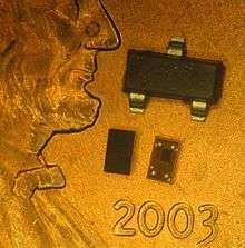
Example WL-CSP devices sitting on the face of a
U.S. penny. A
SOT-23 device is shown for comparison.
| Acronym | Full name | Remark |
| CSP | Chip-scale package | Package size is no more than 1.2× the size of the silicon chip[16][17] |
| TCSP | True chip-size package | Package is same size as silicon[18] |
| TDSP | True die-size package | Same as TCSP[18] |
| WCSP | Wafer-level chip-scale package |
|
| MICRO SMD | - | Chip-size package (CSP) developed by National Semiconductor[19] |
| COB | Chip-on-board | Bare silicon chip, that is usually an integrated circuit, is supplied without a package. |
| COF | Chip-on-flex | Variation of COB, where a chip is mounted directly to a flex circuit. |
| COG | Chip-on-glass | Variation of COB, where a chip is mounted directly to a piece of glass - typically an LCD. |
Ball grid array
Ball Grid Array BGA uses the underside of the package to place pads with balls of solder in grid pattern as connections to PCB.[1][3]
| Acronym | Full name | Remark |
| FBGA | Fine-pitch ball-grid array | A square or rectangular array of solder balls on one surface[3] |
| LBGA | Low-profile ball-grid array | Also known as laminate ball-grid array[3] |
| TEPBGA | Thermally-enhanced plastic ball-grid array | - |
| CBGA | Ceramic ball-grid array[3] | - |
| OBGA | Organic ball-grid array[3] | - |
| TFBGA | Thin fine-pitch ball-grid array[3] | - |
| PBGA | Plastic ball-grid array[3] | - |
| MAP-BGA | Mold array process - ball-grid array | - |
| UCSP | Micro (μ) chip-scale package | Similar to a BGA (A Maxim trademark example)[17] |
| μBGA | Micro ball-grid array | Ball spacing less than 1 mm |
| LFBGA | Low-profile fine-pitch ball-grid array[3] | - |
| TBGA | Thin ball-grid array[3] | - |
| SBGA | Super ball-grid array[3] | Above 500 balls |
| UFBGA | Ultra-fine ball-grid array[3] | |
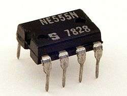
Transistor, diode, small-pin-count IC packages
- MELF: Metal electrode leadless face (usually for resistors and diodes)
- SOD: Small-outline diode.
- SOT: Small-outline transistor (also SOT-23, SOT-223, SOT-323).
- TO-XX: wide range of small pin count packages often used for discrete parts like transistors or diodes.
- TO-3: Panel-mount with leads
- TO-5: Metal can package with radial leads
- TO-18: Metal can package with radial leads
- TO-39
- TO-46
- TO-66: Similar shape to the TO-3 but smaller
- TO-92: Plastic-encapsulated package with three leads
- TO-99
- TO-100
- TO-126: Plastic-encapsulated package with three leads and a hole for mounting on a heat sink
- TO-220: Through-hole plastic package with a (usually) metal heat sink tab and three leads
- TO-226[20]
- TO-247:[21] Plastic-encapsulated package with three leads and a hole for mounting on a heat sink
- TO-251:[21] Also called IPAK: SMT package similar to the DPAK but with longer leads for SMT or TH mounting
- TO-252:[21] (also called SOT428, DPAK):[21] SMT package similar to the DPAK but smaller
- TO-262:[21] Also called I2PAK: SMT package similar to the D2PAK but with longer leads for SMT or TH mounting
- TO-263:[21] Also called D2PAK: SMT package similar to the TO-220 without the extended tab and mounting hole
- TO-274:[21] Also called Super-247: SMT package similar to the TO-247 without the mounting hole
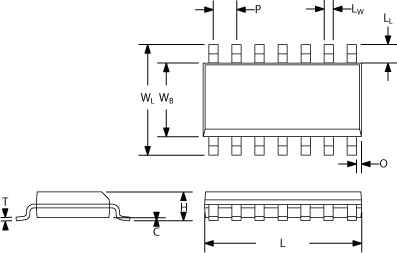
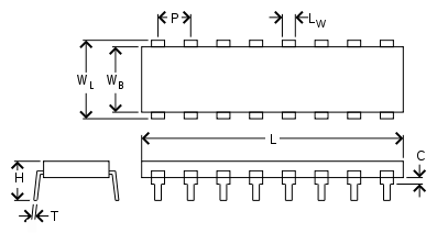
Dimension reference
Surface-mount
- C
- Clearance between IC body and PCB
- H
- Total Height
- T
- Lead Thickness
- L
- Total carrier length
- LW
- Lead width
- LL
- Lead length
- P
- Pitch
Through-hole
- C
- Clearance between IC body and board
- H
- Total height
- T
- Lead thickness
- L
- Total carrier length
- LW
- Lead width
- LL
- Lead length
- P
- Pitch
- WB
- IC body width
- WL
- Lead-to-lead width
Multi-chip packages
A variety of techniques for interconnecting several chips within a single package have been proposed and researched:
References
- 1 2 3 4 5 6 7 8 9 10 11 12 13 14 15 "CPU Collection Museum - Chip Package Information". The CPU Shack. Retrieved 2011-12-15.
- ↑ "Archived copy" (PDF). Archived from the original (PDF) on 2011-08-15. Retrieved 2011-02-03.
- 1 2 3 4 5 6 7 8 9 10 11 12 13 14 15 16 17 18 19 20 21 22 23 24 25 26 27 28 29 30 31 32 33 34 35 36 37 38 39 "Integrated Circuit, IC Package Types; SOIC. Surface Mount Device Package". Interfacebus.com. Retrieved 2011-12-15.
- ↑ "National Semiconductor CERPACK Package Products". National.com. Archived from the original on 2012-02-18. Retrieved 2011-12-15.
- ↑ "National Semiconductor CQGP Package Products". National.com. Archived from the original on 2007-10-21. Retrieved 2011-12-15.
- ↑ "National's LLP Package". National.com. Archived from the original on 2011-02-13. Retrieved 2011-12-15.
- ↑ "LTCC Low Temperature Co-fired Ceramic". Minicaps.com. Retrieved 2011-12-15.
- ↑ "IEEE Xplore - Performance evaluation of MCM chip-to-chip interconnections using custom I/O buffer designs". Ieeexplore.ieee.org. doi:10.1109/ASIC.1993.410760. Retrieved 2011-12-15.
- ↑ "National Semiconductor Launches New Generation of Ultra-Miniature, High Pin-Count Integrated Circuit Packages". National.com. Retrieved 2011-12-15.
- ↑ Meyers, Michael; Jernigan, Scott (2004). Mike Meyers' A+ Guide to PC Hardware. The McGraw-Hill Companies. ISBN 978-0-07-223119-9.
- ↑ Archived August 18, 2011, at the Wayback Machine.
- ↑ "Press Releases - Motorola Mobility, Inc". Motorola.com. Retrieved 2011-12-15.
- ↑ "Xilinx new CPLDs with two I/O banks". Eetasia.com. 2004-12-08. Retrieved 2011-12-15.
- ↑ "Packages". Chelseatech.com. 2010-11-15. Retrieved 2011-12-15.
- ↑ "Archived copy". Archived from the original on 2008-11-20. Retrieved 2009-10-24.
- ↑ "CSP - Chip Scale Package". Siliconfareast.com. Retrieved 2011-12-15.
- 1 2 "Understanding Flip-Chip and Chip-Scale Package Technologies and Their Applications - Maxim". Maxim-ic.com. 2007-04-18. Retrieved 2011-12-15.
- 1 2 "Chip Scale Review Online". Chipscalereview.com. Retrieved 2011-12-15.
- ↑ "Packaging Technology | National Semiconductor – Package Drawings, Part Marking, Package Codes, LLP, micro SMD, Micro-Array". National.com. Archived from the original on 2010-08-01. Retrieved 2011-12-15.
- ↑ http://www.siliconfareast.com/to226.htm
- 1 2 3 4 5 6 7 http://www.irf.com/package/
- ↑ http://pdfserv.maximintegrated.com/package_dwgs/21-0036.PDF
- ↑ "Fairchild's TinyLogic family overview" (PDF). March 22, 2013. Archived from the original (PDF) on January 8, 2015.
- ↑
Proximity Communication - the Technology, 2004, archived from the original on 2009-07-18
External links
|
|---|
| Diode |
- DO-204 (DO-7 / DO-35 / DO-41)
- DO-213 (MELF)
- DO-214 (SMA / SMB / SMC)
- SOD (SOD-123 / SOD-323 / SOD-523 / SOD-923)
|
|---|
| Transistor |
- SOT / TSOT
- TO-3 (TH / Panel)
- TO-5 (TH)
- TO-18 (TH)
- TO-39 (TH)
- TO-66 (TH / Panel)
- TO-92 (TH)
- TO-126 (TH / Panel)
- TO-202 (TH / Panel)
- TO-220 (TH / Panel)
- TO-247 (TH / Panel)
- TO-251 (IPAK) (SMT)
- TO-252 (DPAK) (SMT)
- TO-262 (I2PAK) (SMT)
- TO-263 (D2PAK) (SMT)
- TO-273 (Super-220) (SMT)
- TO-274 (Super-247) (SMT)
|
|---|
| Single row | |
|---|
| Dual row | |
|---|
| Quad row | |
|---|
| Grid array | |
|---|
| Wafer | |
|---|
| Related topics | |
|---|
Note: It's relatively common to find packages that contain other components than their designated ones, such as diodes or voltage regulators in transistor packages, etc. |
.svg.png)


