Memory cell (computing)
| Computer memory types |
|---|
| Volatile |
| RAM |
| Historical |
|
| Non-volatile |
| ROM |
| NVRAM |
| Early stage NVRAM |
| Magnetic |
| Optical |
| In development |
| Historical |
|
The memory cell is the fundamental building block of computer memory. The memory cell is an electronic circuit that stores one bit of binary information and it must be set to store a logic 1 (high voltage level) and reset to store a logic 0 (low voltage level). Its value is maintained/stored until it is changed by the set/reset process. The value in the memory cell can be accessed by reading it.
Over the history of computing many different memory cell architectures have been used including core memory and bubble memory, but the most common ones used are flip-flops and capacitors.
The SRAM, static ram memory cell is a type of flip-flop circuit, usually implemented using FETs. These require very low power to keep the stored value when not being accessed.
A second type, DRAM is based around a capacitor. Charging and discharging this capacitor can store a '1' or a '0' in the cell. However, the charge in this capacitor will slowly leak away, and must be refreshed periodically. Because of this refresh process, DRAM uses more power, but can achieve greater storage densities.
Description
The memory cell is the fundamental building block of memory. It can be implemented using different technologies, such as bipolar, MOS, and other semiconductor devices. It can also be built from magnetic material such as ferrite cores or magnetic bubbles.[1] Regardless of the implementation technology used, the purpose of the binary memory cell is always the same. It stores one bit of binary information that can be accessed by reading the cell and it must be set to store a 1 and reset to store a 0.[2]
Significance
Logic circuits without memory cells or feedback paths are called combinational, their outputs values depend only on the current value of their input values. They do not have memory. But memory is a key element of digital systems. In computers, it allows to store both programs and data and memory cells are also used for temporary storage of the output of combinational circuits to be used later by digital systems. Logic circuits that use memory cells are called sequential circuits. Its output depends not only on the present value of its inputs, but also on the circuits previous state, as determined by the values stored on is memory cells. These circuits require a timing generator or clock for their operation.[3]
Computer memory used in most contemporary computer systems is built mainly out of DRAM cells, since the layout is much smaller than SRAM, it can be more densely packed yielding cheaper memory with greater capacity. Since the DRAM memory cell stores its value as the charge of a capacitor, and there are current leakage issues, its value must be constantly rewriten. this is one of the reasons that make DRAM cells slower than the larger SRAM (Static RAM) cells, which has its value always available. That is the reason why SRAM memory is used for on-chip cache included in modern microprocessor chips.[4]
History
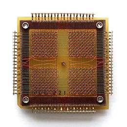
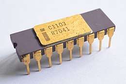
On December 11, 1946 Freddie Williams applied for a patent on his cathode-ray tube (CRT) storing device (Williams tube) with 128 40-bit words. It was operational in 1947 and is considered the first practical implementation of random-access memory.[5] In that year, the first patent applications for magnetic-core memory were filed by Frederick Viehe.[6][7] An Wang, Ken Olsen and Jay Forrester also contributed to its development.[8] The first modern memory cells were introduced in 1965, when John Schmidt designed the first 64-bit MOS p-channel SRAM.[9] The first bipolar 64-bit SRAM was released by Intel in 1969 with the 3101 Schottky TTL. One year later it released the first DRAM chip, the Intel 1103 that by 1972 beat all worldwide records in semiconductor memory sales.[10]
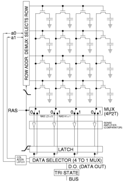
Implementation
The following schematics detail the three most used implementations for memory cells :
- The Dynamic Random Access Memory cell (DRAM)
- The Static Random Access Memory cell (SRAM)
- Flip flops like the J/K shown below.
.PNG) DRAM Cell (1 Transistor and one capacitor) | SRAM Cell (6 Transistors) | 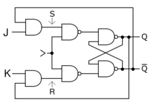 Clocked J/K flip flop |
Operation
DRAM memory cell
Storage
- The storage element of the DRAM memory cell is the capacitor labeled (4) in the diagram above. The charge stored in the capacitor degrades over time, so its value must be refreshed (read and rewritten) periodically. The nMOS transistor (3) acts as a gate to allow reading or writing when open or storing when closed.[11]
Reading
- For reading the Word line drives a logic 1 (voltage high) into the gate of the nMOS transistor (3) which makes it conductive and the charge stored at the capacitor (4) is then transferred to the bit line. The bit line will have a parasitic capacitance (5) that will drain part of the charge and slow the reading process. The capacitance of the bit line will determine the needed size of the storage capacitor (4). It is a trade-off. If the storage capacitor is too small, the voltage of the bit line would take too much time to raise or not even rise above the threshold needed by the amplifiers at the end of the bit line. Since the reading process degrades the charge in the storage capacitor (4) its value is rewritten after each read.[12]
Writing
- The writing process is the easiest, the desired value logic 1 (high voltage) or logic 0 (low voltage) is driven into the bit line. The word line activates the nMOS transistor (3) connecting it to the storage capacitor (4). The only issue is to keep it open enough time to ensure that the capacitor is fully charged or discharged before turning off the nMOS transistor (3).[12]
SRAM memory cell
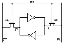
Storage
- The working principle of SRAM memory cell can be easier to understand if the transistors M1 through M4 are drawn as logic gates. That way it is clear that at its heart, the cell storage is built by using two cross-coupled inverters. This simple loop, creates a bi-stable circuit. A logic 1 at the input of the first inverter turns into a 0 at its output, and it is fed into the second inverter which transforms that logic 0 back to a logic 1 feeding back the same value to the input of the first inverter. That creates a stable state that does not change over time. Similarly the other stable state of the circuit is to have a logic 0 at the input of the first inverter. After been inverted twice it will also feedback the same value.[13]
- Therefore there are only two stable states that the circuit can be in:
- = 0 and = 1
- = 1 and = 0


Reading
- To read the contents of the memory cell stored in the loop, the transistors M5 and M6 must be turned on. when they receive voltage to their gates from the word line ( ), they become conductive and so the and values get transmitted to the bit line ( ) and to its complement ( ).[13] Finally this values get amplified at the end of the bit lines.[13]


Writing
- The writing process is similar, the difference is that now the new value that will be stored in the memory cell is driven into the bit line (
) and the inverted one into its complement (
). Next transistors M5 and M6 are open by driving a logic one (voltage high) into the word line (
). This effectively connects the bit lines to the by-stable inverter loop. There are two possible cases:
- If the value of the loop is the same as the new value driven, there is no change.
- If the value of the loop is different from the new value driven there are two conflicting values, in order for the voltage in the bit lines to overwrite the output of the inverters, the size of the M5 and M6 transistors must be larger than that of the M1-M4 transistors. This allow more current to flow through first ones and therefore tips the voltage in the direction of the new value, at some point the loop will then amplify this intermediate value to full rail.[13]
Flip flop
The flip-flop has many different implementations, its storage element is usually a Latch consisting of a NAND gate loop or a NOR gate loop with additional gates used to implement clocking. Its value is always available for reading as an output. The value remains stored until it is changed through the set or reset process.
See also
References
- ↑ D. Tang, Denny; Lee, Yuan-Jen (2010). Magnetic Memory: Fundamentals and Technology. Cambridge University Press. p. 91. ISBN 1139484494. Retrieved 13 December 2015.
- ↑ Fletcher, William (1980). An engineering approach to digital design. Prentice-Hall. p. 283. ISBN 0-13-277699-5.
- ↑ Microelectronic Circuits (Second ed.). Holt, Rinehart and Winston, Inc. 1987. p. 883. ISBN 0-03-007328-6.
- ↑ "La Question Technique : le cache, comment ça marche ?". PC World Fr. Archived from the original on 2014-03-30.
- ↑ O’Regan, Gerard (2013). Giants of Computing: A Compendium of Select, Pivotal Pioneers. Springer Science & Business Media. p. 267. ISBN 1447153405. Retrieved 13 December 2015.
- ↑ Reilly, Edwin D. (2003). Milestones in Computer Science and Information Technology. Greenwood Publishing Group. p. 164. ISBN 9781573565219.
- ↑ W. Pugh, Emerson; R. Johnson, Lyle; H. Palmer, John (1991). IBM's 360 and Early 370 Systems. MIT Press. p. 706. ISBN 0262161230. Retrieved 9 December 2015.
- ↑ Taylor, Alan (18 June 1979). Computerworld: Mass. Town has become computer capital. IDG Enterprise. p. 25.
- ↑ Solid State Design - Vol. 6. Horizon House. 1965.
- ↑ Kent, Allen; Williams, James G. (6 January 1992). Encyclopedia of Microcomputers: Volume 9 - Icon Programming Language to Knowledge-Based Systems: APL Techniques. CRC Press. p. 131. ISBN 9780824727086.
- ↑ Jacob, Bruce; Ng, Spencer; Wang, David (28 July 2010). Memory Systems: Cache, DRAM, Disk. Morgan Kaufmann. p. 355. ISBN 9780080553849.
- 1 2 Siddiqi, Muzaffer A. (19 December 2012). Dynamic RAM: Technology Advancements. CRC Press. p. 10. ISBN 9781439893739.
- 1 2 3 4 Li, Hai; Chen, Yiran (19 April 2016). Nonvolatile Memory Design: Magnetic, Resistive, and Phase Change. CRC Press. pp. 6, 7. ISBN 9781439807460.