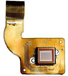
Image sensor
An image sensor or imager is a sensor that detects and conveys information used to make an image. It does so by converting the variable attenuation of light waves (as they pass through or reflect off objects) into signals, small bursts of current that convey the information. The waves can be light or other electromagnetic radiation. Image sensors are used in electronic imaging devices of both analog and digital types, which include digital cameras, camera modules, camera phones, optical mouse devices,[1][2][3] medical imaging equipment, night vision equipment such as thermal imaging devices, radar, sonar, and others. As technology changes, electronic and digital imaging tends to replace chemical and analog imaging.
The two main types of electronic image sensors are the charge-coupled device (CCD) and the active-pixel sensor (CMOS sensor). Both CCD and CMOS sensors are based on metal–oxide–semiconductor (MOS) technology, with CCDs based on MOS capacitors and CMOS sensors based on MOSFET (MOS field-effect transistor) amplifiers. Analog sensors for invisible radiation tend to involve vacuum tubes of various kinds. Digital sensors include flat-panel detectors.
CCD vs. CMOS sensors
The two main types of digital image sensors are the charge-coupled device (CCD) and the active-pixel sensor (CMOS sensor), fabricated in complementary MOS (CMOS) or N-type MOS (NMOS or Live MOS) technologies. Both CCD and CMOS sensors are based on MOS technology,[4] with MOS capacitors being the building blocks of a CCD,[5] and MOSFET amplifiers being the building blocks of a CMOS sensor.[6][7]
Cameras integrated in small consumer products generally use CMOS sensors, which are usually cheaper and have lower power consumption in battery powered devices than CCDs.[8] CCD sensors are used for high end broadcast quality video cameras, and (C)MOS sensors dominate in still photography and consumer goods where overall cost is a major concern. Both types of sensor accomplish the same task of capturing light and converting it into electrical signals.
Each cell of a CCD image sensor is an analog device. When light strikes the chip it is held as a small electrical charge in each photo sensor. The charges in the line of pixels nearest to the (one or more) output amplifiers are amplified and output, then each line of pixels shifts its charges one line closer to the amplifier(s), filling the empty line closest to the amplifiers(s). This process is then repeated until all the lines of pixels have had their charge amplified and output.[9]
A CMOS image sensor has an amplifier for each pixel compared to the few amplifiers of a CCD. This results in less area for the capture of photons than a CCD, but this problem has been overcome by using microlenses in front of each photodiode, which focus light into the photodiode that would have otherwise hit the amplifier and not been detected.[9] Some CMOS imaging sensors also use Back-side illumination to increase the number of photons that hit the photodiode.[10] CMOS sensors can potentially be implemented with fewer components, use less power, and/or provide faster readout than CCD sensors.[11] They are also less vulnerable to static electricity discharges.
Another design, a hybrid CCD/CMOS architecture (sold under the name "sCMOS") consists of CMOS readout integrated circuits (ROICs) that are bump bonded to a CCD imaging substrate – a technology that was developed for infrared staring arrays and has been adapted to silicon-based detector technology.[12] Another approach is to utilize the very fine dimensions available in modern CMOS technology to implement a CCD like structure entirely in CMOS technology: such structures can be achieved by separating individual poly-silicon gates by a very small gap; though still a product of research hybrid sensors can potentially harness the benefits of both CCD and CMOS imagers.[13]
Performance
There are many parameters that can be used to evaluate the performance of an image sensor, including dynamic range, signal-to-noise ratio, and low-light sensitivity. For sensors of comparable types, the signal-to-noise ratio and dynamic range improve as the size increases.
Exposure-time control
Exposure time of image sensors is generally controlled by either a conventional mechanical shutter, as in film cameras, or by an electronic shutter. Electronic shuttering can be "global", in which case the entire image sensor area's accumulation of photoelectrons starts and stops simultaneously, or "rolling" in which case the exposure interval of each row immediate precedes that row's readout, in a process that "rolls" across the image frame (typically from top to bottom in landscape format). Global electronic shuttering is less common, as it requires "storage" circuits to hold charge from the end of the exposure interval until the readout process gets there, typically a few milliseconds later.[14]
Color separation
There are several main types of color image sensors, differing by the type of color-separation mechanism:
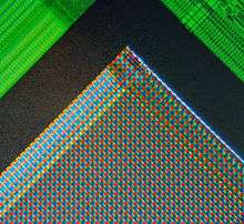
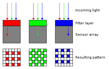
- Bayer-filter sensor, low-cost and most common, using a color filter array that passes red, green, and blue light to selected pixel sensors. Each individual sensor element is made sensitive to red, green, or blue by means of a color gel made of chemical dyes patterned over the elements. The most common filter matrix, the Bayer pattern, uses two green pixels for each red and blue. This results in less resolution for red and blue colors. The missing color samples may interpolated using a demosaicing algorithm, or ignored altogether by lossy compression. In order to improve color information, techniques like color co-site sampling use a piezo mechanism to shift the color sensor in pixel steps.
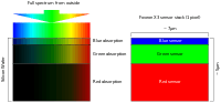
- Foveon X3 sensor, using an array of layered pixel sensors, separating light via the inherent wavelength-dependent absorption property of silicon, such that every location senses all three color channels. This method is similar to how color film for photography works.
- 3CCD, using three discrete image sensors, with the color separation done by a dichroic prism. The dichroic elements provide a sharper color separation, thus improving color quality. Because each sensor is equally sensitive within its passband, and at full resolution, 3-CCD sensors produce better color quality and better low light performance. 3-CCD sensors produce a full 4:4:4 signal, which is preferred in television broadcasting, video editing and chroma key visual effects.
Specialty sensors

Special sensors are used in various applications such as thermography, creation of multi-spectral images, video laryngoscopes, gamma cameras, sensor arrays for x-rays, and other highly sensitive arrays for astronomy.
While in general digital cameras use a flat sensor, Sony prototyped a curved sensor in 2014 to reduce/eliminate Petzval field curvature that occurs with a flat sensor. Use of a curved sensor allows a shorter and smaller diameter of the lens with reduced elements and components with greater aperture and reduced light fall-off at the edge of the photo.[16]
History
Early analog sensors for visible light were video camera tubes. They date back to the 1930s, and several types were developed up until the 1980s. By the early 1990s, they had been replaced by modern solid-state image sensors.[17]
The basis for modern solid-state image sensors is MOS technology,[18][19] which originates from the invention of the MOSFET by Mohamed M. Atalla and Dawon Kahng at Bell Labs in 1959.[20] Later research on MOS technology led to the development of solid-state semiconductor image sensors, including the charge-coupled device (CCD) and later the active-pixel sensor (CMOS sensor).[18][19]
The passive-pixel sensor (PPS) was the precursor to the active-pixel sensor (APS).[7] A PPS consists of passive pixels which are read out without amplification, with each pixel consisting of a photodiode and a MOSFET switch.[21] It is a type of photodiode array, with pixels containing a p-n junction, integrated capacitor, and MOSFETs as selection transistors. A photodiode array was proposed by G. Weckler in 1968.[6] This was the basis for the PPS.[7] These early photodiode arrays were complex and impractical, requiring selection transistors to be fabricated within each pixel, along with on-chip multiplexer circuits. The noise of photodiode arrays was also a limitation to performance, as the photodiode readout bus capacitance resulted in increased noise level. Correlated double sampling (CDS) could also not be used with a photodiode array without external memory.[6]
Charge-coupled device
The charge-coupled device (CCD) was invented by Willard S. Boyle and George E. Smith at Bell Labs in 1969.[22] While researching MOS technology, they realized that an electric charge was the analogy of the magnetic bubble and that it could be stored on a tiny MOS capacitor. As it was fairly straighforward to fabricate a series of MOS capacitors in a row, they connected a suitable voltage to them so that the charge could be stepped along from one to the next.[18] The CCD is a semiconductor circuit that was later used in the first digital video cameras for television broadcasting.[23]
Early CCD sensors suffered from shutter lag. This was largely resolved with the invention of the pinned photodiode (PPD).[7] It was invented by Nobukazu Teranishi, Hiromitsu Shiraki and Yasuo Ishihara at NEC in 1980.[7][24] It was a photodetector structure with low lag, low noise, high quantum efficiency and low dark current.[7] In 1987, the PPD began to be incorporated into most CCD devices, becoming a fixture in consumer electronic video cameras and then digital still cameras. Since then, the PPD has been used in nearly all CCD sensors and then CMOS sensors.[7]
Active-pixel sensor
The NMOS active-pixel sensor (APS) was invented by Olympus in Japan during the mid-1980s. This was enabled by advances in MOS semiconductor device fabrication, with MOSFET scaling reaching smaller micron and then sub-micron levels.[6][25] The first NMOS APS was fabricated by Tsutomu Nakamura's team at Olympus in 1985.[26] The CMOS active-pixel sensor (CMOS sensor) was later developed by Eric Fossum's team at the NASA Jet Propulsion Laboratory in 1993.[7] By 2007, sales of CMOS sensors had surpassed CCD sensors.[27]
Other image sensors
The first commercial digital camera, the Cromemco Cyclops in 1975, used a 32×32 MOS image sensor. It was a modified MOS dynamic RAM (DRAM) memory chip.[28]
MOS image sensors are widely used in optical mouse technology. The first optical mouse, invented by Richard F. Lyon at Xerox in 1980, used a 5 µm NMOS integrated circuit sensor chip.[29][30] Since the first commercial optical mouse, the IntelliMouse introduced in 1999, most optical mouse devices use CMOS sensors.[31]
In February 2018, researchers at Dartmouth College announced a new image sensing technology that the researchers call QIS, for Quanta Image Sensor. Instead of pixels, QIS chips have what the researchers call "jots." Each jot can detect a single particle of light, called a photon.[32]
See also
- List of sensors used in digital cameras
- Contact image sensor (CIS)
- Video camera tube
- Semiconductor detector
- Fill factor
- Full-frame digital SLR
- Image sensor format, the sizes and shapes of common image sensors
- Color filter array, mosaic of tiny color filters over color image sensors
- Sensitometry, the scientific study of light-sensitive materials
- History of television, the development of electronic imaging technology since the 1880s
- List of large sensor interchangeable-lens video cameras
- Oversampled binary image sensor
- Computer vision
References
- Lyon, Richard F. (August 1981). "The Optical Mouse, and an Architectural Methodology for Smart Digital Sensors" (PDF). In H. T. Kung; Robert F. Sproull; Guy L. Steele (eds.). VLSI Systems and Computations. Computer Science Press. pp. 1–19. doi:10.1007/978-3-642-68402-9_1. ISBN 978-3-642-68404-3.
- Lyon, Richard F. (2014). "The Optical Mouse: Early Biomimetic Embedded Vision". Advances in Embedded Computer Vision. Springer. pp. 3-22 (3). ISBN 9783319093871.
- Brain, Marshall; Carmack, Carmen (24 April 2000). "How Computer Mice Work". HowStuffWorks. Retrieved 9 October 2019.
- Cressler, John D. (2017). "Let There Be Light: The Bright World of Photonics". Silicon Earth: Introduction to Microelectronics and Nanotechnology, Second Edition. CRC Press. p. 29. ISBN 978-1-351-83020-1.
- Sze, Simon Min; Lee, Ming-Kwei (May 2012). "MOS Capacitor and MOSFET". Semiconductor Devices: Physics and Technology : International Student Version. John Wiley & Sons. ISBN 9780470537947. Retrieved 6 October 2019.
- Fossum, Eric R. (12 July 1993). Blouke, Morley M. (ed.). "Active pixel sensors: are CCDs dinosaurs?". SPIE Proceedings Vol. 1900: Charge-Coupled Devices and Solid State Optical Sensors III. International Society for Optics and Photonics. 1900: 2–14. Bibcode:1993SPIE.1900....2F. CiteSeerX 10.1.1.408.6558. doi:10.1117/12.148585.
- Fossum, Eric R.; Hondongwa, D. B. (2014). "A Review of the Pinned Photodiode for CCD and CMOS Image Sensors". IEEE Journal of the Electron Devices Society. 2 (3): 33–43. doi:10.1109/JEDS.2014.2306412.
- "CMOS Is Winning the Camera Sensor Battle, and Here's Why". techhive.com. 2011-12-29. Archived from the original on 2017-05-01. Retrieved 2017-04-27.
- 2002-2017., Canon Europa N.V. and Canon Europe Ltd. "CCD and CMOS sensors - Canon Professional Network". Canon Professional Network. Archived from the original on 28 April 2018. Retrieved 28 April 2018.CS1 maint: numeric names: authors list (link)
- "What is a backlit CMOS sensor?". techradar.com. 2012-07-02. Archived from the original on 2017-05-06. Retrieved 2017-04-27.
- Moynihan, Tom. "CMOS Is Winning the Camera Sensor Battle, and Here's Why". Archived from the original on 25 September 2015. Retrieved 10 April 2015.
- scmos.com Archived 2012-06-03 at the Wayback Machine, home page
- ieee.org - CCD in CMOS Archived 2015-06-22 at the Wayback Machine Padmakumar R. Rao et al., "CCD structures implemented in standard 0.18 µm CMOS technology"
- Nakamura, Junichi (2005). Image Sensors and Signal Processing for Digital Still Cameras. CRC Press. pp. 169–172. ISBN 9781420026856.
- "Deepest Ever Look into Orion". Archived from the original on 13 July 2016. Retrieved 13 July 2016.
- Steve Dent. "Sony's first 'curved sensor' photo may herald better images, cheaper lenses". Archived from the original on July 11, 2014. Retrieved July 8, 2014.
- Musburger, Robert B.; Ogden, Michael R. (2014). Single-Camera Video Production. CRC Press. p. 64. ISBN 9781136778445.
- Williams, J. B. (2017). The Electronics Revolution: Inventing the Future. Springer. pp. 245–8. ISBN 9783319490885.
- Ohta, Jun (2017). Smart CMOS Image Sensors and Applications. CRC Press. p. 2. ISBN 9781420019155.
- "1960: Metal Oxide Semiconductor (MOS) Transistor Demonstrated". The Silicon Engine. Computer History Museum. Retrieved August 31, 2019.
- Kozlowski, L. J.; Luo, J.; Kleinhans, W. E.; Liu, T. (14 September 1998). "Comparison of passive and active pixel schemes for CMOS visible imagers". Infrared Readout Electronics IV. International Society for Optics and Photonics. 3360: 101–110. Bibcode:1998SPIE.3360..101K. doi:10.1117/12.584474.
- James R. Janesick (2001). Scientific charge-coupled devices. SPIE Press. pp. 3–4. ISBN 978-0-8194-3698-6.
- Boyle, William S; Smith, George E. (1970). "Charge Coupled Semiconductor Devices". Bell Syst. Tech. J. 49 (4): 587–593. doi:10.1002/j.1538-7305.1970.tb01790.x.
- U.S. Patent 4,484,210: Solid-state imaging device having a reduced image lag
- Fossum, Eric R. (2007). "Active Pixel Sensors" (PDF). Semantic Scholar. Retrieved 8 October 2019.
- Matsumoto, Kazuya; et al. (1985). "A new MOS phototransistor operating in a non-destructive readout mode". Japanese Journal of Applied Physics. 24 (5A): L323. Bibcode:1985JaJAP..24L.323M. doi:10.1143/JJAP.24.L323.
- "CMOS Image Sensor Sales Stay on Record-Breaking Pace". IC Insights. May 8, 2018. Retrieved 6 October 2019.
- Benchoff, Brian (17 April 2016). "Building the First Digital Camera". Hackaday. Retrieved 30 April 2016.
the Cyclops was the first digital camera
- Lyon, Richard F. (2014). "The Optical Mouse: Early Biomimetic Embedded Vision". Advances in Embedded Computer Vision. Springer. pp. 3-22 (3). ISBN 9783319093871.
- Lyon, Richard F. (August 1981). "The Optical Mouse, and an Architectural Methodology for Smart Digital Sensors" (PDF). In H. T. Kung; Robert F. Sproull; Guy L. Steele (eds.). VLSI Systems and Computations. Computer Science Press. pp. 1–19. doi:10.1007/978-3-642-68402-9_1. ISBN 978-3-642-68404-3.
- Brain, Marshall; Carmack, Carmen (24 April 2000). "How Computer Mice Work". HowStuffWorks. Retrieved 9 October 2019.
- "Super Sensitive Sensor Sees What You Can't". npr.org. Archived from the original on 24 March 2018. Retrieved 28 April 2018.
External links
- Digital Camera Sensor Performance Summary by Roger Clark
| Authority control |
|
|---|