Microelectromechanical systems
Microelectromechanical systems (MEMS), also written as micro-electro-mechanical systems (or microelectronic and microelectromechanical systems) and the related micromechatronics and microsystems constitute the technology of microscopic devices, particularly those with moving parts. They merge at the nanoscale into nanoelectromechanical systems (NEMS) and nanotechnology. MEMS are also referred to as micromachines in Japan and microsystem technology (MST) in Europe.
MEMS are made up of components between 1 and 100 micrometers in size (i.e., 0.001 to 0.1 mm), and MEMS devices generally range in size from 20 micrometres to a millimetre (i.e., 0.02 to 1.0 mm), although components arranged in arrays (e.g., digital micromirror devices) can be more than 1000 mm2.[1] They usually consist of a central unit that processes data (an integrated circuit chip such as microprocessor) and several components that interact with the surroundings (such as microsensors).[2] Because of the large surface area to volume ratio of MEMS, forces produced by ambient electromagnetism (e.g., electrostatic charges and magnetic moments), and fluid dynamics (e.g., surface tension and viscosity) are more important design considerations than with larger scale mechanical devices. MEMS technology is distinguished from molecular nanotechnology or molecular electronics in that the latter must also consider surface chemistry.
The potential of very small machines was appreciated before the technology existed that could make them (see, for example, Richard Feynman's famous 1959 lecture There's Plenty of Room at the Bottom). MEMS became practical once they could be fabricated using modified semiconductor device fabrication technologies, normally used to make electronics.[3] These include molding and plating, wet etching (KOH, TMAH) and dry etching (RIE and DRIE), electrical discharge machining (EDM), and other technologies capable of manufacturing small devices.
History
MEMS technology has roots in the silicon revolution, which can be traced back to two important silicon semiconductor inventions from 1959: the monolithic integrated circuit (IC) chip by Robert Noyce at Fairchild Semiconductor, and the MOSFET (metal-oxide-semiconductor field-effect transistor, or MOS transistor) by Mohamed M. Atalla and Dawon Kahng at Bell Labs. MOSFET scaling, the miniaturisation of MOSFETs on IC chips, led to the miniaturisation of electronics (as predicted by Moore's law and Dennard scaling). This laid the foundations for the miniaturisation of mechanical systems, with the development of micromachining technology based on silicon semiconductor technology, as engineers began realizing that silicon chips and MOSFETs could interact and communicate with the surroundings and process things such as chemicals, motions and light. One of the first silicon pressure sensors was isotropically micromachined by Honeywell in 1962.[4]
An early example of a MEMS device is the resonant-gate transistor, an adaptation of the MOSFET, developed by Harvey C. Nathanson in 1965.[5] Another early example is the resonistor, an electromechanical monolithic resonator patented by Raymond J. Wilfinger between 1966 and 1971.[6][7] During the 1970s to early 1980s, a number of MOSFET microsensors were developed for measuring physical, chemical, biological and environmental parameters.[8]
Types
There are two basic types of MEMS switch technology: capacitive and ohmic. A capacitive MEMS switch is developed using a moving plate or sensing element, which changes the capacitance.[9] Ohmic switches are controlled by electrostatically controlled cantilevers.[10] Ohmic MEMS switches can fail from metal fatigue of the MEMS actuator (cantilever) and contact wear, since cantilevers can deform over time.[11]
Materials for MEMS manufacturing
The fabrication of MEMS evolved from the process technology in semiconductor device fabrication, i.e. the basic techniques are deposition of material layers, patterning by photolithography and etching to produce the required shapes.[12]
Silicon
Silicon is the material used to create most integrated circuits used in consumer electronics in the modern industry. The economies of scale, ready availability of inexpensive high-quality materials, and ability to incorporate electronic functionality make silicon attractive for a wide variety of MEMS applications. Silicon also has significant advantages engendered through its material properties. In single crystal form, silicon is an almost perfect Hookean material, meaning that when it is flexed there is virtually no hysteresis and hence almost no energy dissipation. As well as making for highly repeatable motion, this also makes silicon very reliable as it suffers very little fatigue and can have service lifetimes in the range of billions to trillions of cycles without breaking. Semiconductor nanostructures based on silicon are gaining increasing importance in the field of microelectronics and MEMS in particular. Silicon nanowires, fabricated through the thermal oxidation of silicon, are of further interest in electrochemical conversion and storage, including nanowire batteries and photovoltaic systems.
Polymers
Even though the electronics industry provides an economy of scale for the silicon industry, crystalline silicon is still a complex and relatively expensive material to produce. Polymers on the other hand can be produced in huge volumes, with a great variety of material characteristics. MEMS devices can be made from polymers by processes such as injection molding, embossing or stereolithography and are especially well suited to microfluidic applications such as disposable blood testing cartridges.
Metals
Metals can also be used to create MEMS elements. While metals do not have some of the advantages displayed by silicon in terms of mechanical properties, when used within their limitations, metals can exhibit very high degrees of reliability. Metals can be deposited by electroplating, evaporation, and sputtering processes. Commonly used metals include gold, nickel, aluminium, copper, chromium, titanium, tungsten, platinum, and silver.
Ceramics
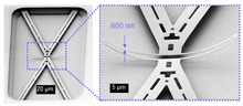
The nitrides of silicon, aluminium and titanium as well as silicon carbide and other ceramics are increasingly applied in MEMS fabrication due to advantageous combinations of material properties. AlN crystallizes in the wurtzite structure and thus shows pyroelectric and piezoelectric properties enabling sensors, for instance, with sensitivity to normal and shear forces.[14] TiN, on the other hand, exhibits a high electrical conductivity and large elastic modulus, making it possible to implement electrostatic MEMS actuation schemes with ultrathin beams. Moreover, the high resistance of TiN against biocorrosion qualifies the material for applications in biogenic environments. The figure shows an electron-microscopic picture of a MEMS biosensor with a 50 nm thin bendable TiN beam above a TiN ground plate. Both can be driven as opposite electrodes of a capacitor, since the beam is fixed in electrically isolating side walls. When a fluid is suspended in the cavity its viscosity may be derived from bending the beam by electrical attraction to the ground plate and measuring the bending velocity. [13]
MEMS basic processes
Deposition processes
One of the basic building blocks in MEMS processing is the ability to deposit thin films of material with a thickness anywhere between one micrometre, to about 100 micrometres. The NEMS process is the same, although the measurement of film deposition ranges from a few nanometres to one micrometre. There are two types of deposition processes, as follows.
Physical deposition
Physical vapor deposition ("PVD") consists of a process in which a material is removed from a target, and deposited on a surface. Techniques to do this include the process of sputtering, in which an ion beam liberates atoms from a target, allowing them to move through the intervening space and deposit on the desired substrate, and evaporation, in which a material is evaporated from a target using either heat (thermal evaporation) or an electron beam (e-beam evaporation) in a vacuum system.
Chemical deposition
Chemical deposition techniques include chemical vapor deposition (CVD), in which a stream of source gas reacts on the substrate to grow the material desired. This can be further divided into categories depending on the details of the technique, for example LPCVD (low-pressure chemical vapor deposition) and PECVD (plasma-enhanced chemical vapor deposition).
Oxide films can also be grown by the technique of thermal oxidation, in which the (typically silicon) wafer is exposed to oxygen and/or steam, to grow a thin surface layer of silicon dioxide.
Patterning
Patterning in MEMS is the transfer of a pattern into a material.
Lithography
Lithography in MEMS context is typically the transfer of a pattern into a photosensitive material by selective exposure to a radiation source such as light. A photosensitive material is a material that experiences a change in its physical properties when exposed to a radiation source. If a photosensitive material is selectively exposed to radiation (e.g. by masking some of the radiation) the pattern of the radiation on the material is transferred to the material exposed, as the properties of the exposed and unexposed regions differs.
This exposed region can then be removed or treated providing a mask for the underlying substrate. Photolithography is typically used with metal or other thin film deposition, wet and dry etching. Sometimes, photolithography is used to create structure without any kind of post etching. One example is SU8 based lens where SU8 based square blocks are generated. Then the photoresist is melted to form a semi-sphere which acts as a lens.
Electron beam lithography
Electron beam lithography (often abbreviated as e-beam lithography) is the practice of scanning a beam of electrons in a patterned fashion across a surface covered with a film (called the resist),[15] ("exposing" the resist) and of selectively removing either exposed or non-exposed regions of the resist ("developing"). The purpose, as with photolithography, is to create very small structures in the resist that can subsequently be transferred to the substrate material, often by etching. It was developed for manufacturing integrated circuits, and is also used for creating nanotechnology architectures.
The primary advantage of electron beam lithography is that it is one of the ways to beat the diffraction limit of light and make features in the nanometer range. This form of maskless lithography has found wide usage in photomask-making used in photolithography, low-volume production of semiconductor components, and research & development.
The key limitation of electron beam lithography is throughput, i.e., the very long time it takes to expose an entire silicon wafer or glass substrate. A long exposure time leaves the user vulnerable to beam drift or instability which may occur during the exposure. Also, the turn-around time for reworking or re-design is lengthened unnecessarily if the pattern is not being changed the second time.
Ion beam lithography
It is known that focused-ion beam lithography has the capability of writing extremely fine lines (less than 50 nm line and space has been achieved) without proximity effect. However, because the writing field in ion-beam lithography is quite small, large area patterns must be created by stitching together the small fields.
Ion track technology
Ion track technology is a deep cutting tool with a resolution limit around 8 nm applicable to radiation resistant minerals, glasses and polymers. It is capable of generating holes in thin films without any development process. Structural depth can be defined either by ion range or by material thickness. Aspect ratios up to several 104 can be reached. The technique can shape and texture materials at a defined inclination angle. Random pattern, single-ion track structures and aimed pattern consisting of individual single tracks can be generated.
X-ray lithography
X-ray lithography is a process used in electronic industry to selectively remove parts of a thin film. It uses X-rays to transfer a geometric pattern from a mask to a light-sensitive chemical photoresist, or simply "resist", on the substrate. A series of chemical treatments then engraves the produced pattern into the material underneath the photoresist.
Diamond patterning
A simple way to carve or create patterns on the surface of nanodiamonds without damaging them could lead to a new photonic devices.
Diamond patterning is a method of forming diamond MEMS. It is achieved by the lithographic application of diamond films to a substrate such as silicon. The patterns can be formed by selective deposition through a silicon dioxide mask, or by deposition followed by micromachining or focused ion beam milling.[16]
Etching processes
There are two basic categories of etching processes: wet etching and dry etching. In the former, the material is dissolved when immersed in a chemical solution. In the latter, the material is sputtered or dissolved using reactive ions or a vapor phase etchant.[17][18]
Wet etching
Wet chemical etching consists in selective removal of material by dipping a substrate into a solution that dissolves it. The chemical nature of this etching process provides a good selectivity, which means the etching rate of the target material is considerably higher than the mask material if selected carefully.
Isotropic etching
Etching progresses at the same speed in all directions. Long and narrow holes in a mask will produce v-shaped grooves in the silicon. The surface of these grooves can be atomically smooth if the etch is carried out correctly, with dimensions and angles being extremely accurate.
Anisotropic etching
Some single crystal materials, such as silicon, will have different etching rates depending on the crystallographic orientation of the substrate. This is known as anisotropic etching and one of the most common examples is the etching of silicon in KOH (potassium hydroxide), where Si <111> planes etch approximately 100 times slower than other planes (crystallographic orientations). Therefore, etching a rectangular hole in a (100)-Si wafer results in a pyramid shaped etch pit with 54.7° walls, instead of a hole with curved sidewalls as with isotropic etching.
HF etching
Hydrofluoric acid is commonly used as an aqueous etchant for silicon dioxide (SiO
2, also known as BOX for SOI), usually in 49% concentrated form, 5:1, 10:1 or 20:1 BOE (buffered oxide etchant) or BHF (Buffered HF). They were first used in medieval times for glass etching. It was used in IC fabrication for patterning the gate oxide until the process step was replaced by RIE.
Hydrofluoric acid is considered one of the more dangerous acids in the cleanroom. It penetrates the skin upon contact and it diffuses straight to the bone. Therefore, the damage is not felt until it is too late.
Electrochemical etching
Electrochemical etching (ECE) for dopant-selective removal of silicon is a common method to automate and to selectively control etching. An active p-n diode junction is required, and either type of dopant can be the etch-resistant ("etch-stop") material. Boron is the most common etch-stop dopant. In combination with wet anisotropic etching as described above, ECE has been used successfully for controlling silicon diaphragm thickness in commercial piezoresistive silicon pressure sensors. Selectively doped regions can be created either by implantation, diffusion, or epitaxial deposition of silicon.
Dry etching
Vapor etching
Xenon difluoride
Xenon difluoride (XeF
2) is a dry vapor phase isotropic etch for silicon originally applied for MEMS in 1995 at University of California, Los Angeles.[19][20] Primarily used for releasing metal and dielectric structures by undercutting silicon, XeF
2 has the advantage of a stiction-free release unlike wet etchants. Its etch selectivity to silicon is very high, allowing it to work with photoresist, SiO
2, silicon nitride, and various metals for masking. Its reaction to silicon is "plasmaless", is purely chemical and spontaneous and is often operated in pulsed mode. Models of the etching action are available,[21] and university laboratories and various commercial tools offer solutions using this approach.
Plasma etching
Modern VLSI processes avoid wet etching, and use plasma etching instead. Plasma etchers can operate in several modes by adjusting the parameters of the plasma. Ordinary plasma etching operates between 0.1 and 5 Torr. (This unit of pressure, commonly used in vacuum engineering, equals approximately 133.3 pascals.) The plasma produces energetic free radicals, neutrally charged, that react at the surface of the wafer. Since neutral particles attack the wafer from all angles, this process is isotropic.
Plasma etching can be isotropic, i.e., exhibiting a lateral undercut rate on a patterned surface approximately the same as its downward etch rate, or can be anisotropic, i.e., exhibiting a smaller lateral undercut rate than its downward etch rate. Such anisotropy is maximized in deep reactive ion etching. The use of the term anisotropy for plasma etching should not be conflated with the use of the same term when referring to orientation-dependent etching.
The source gas for the plasma usually contains small molecules rich in chlorine or fluorine. For instance, carbon tetrachloride (CCl
4) etches silicon and aluminium, and trifluoromethane etches silicon dioxide and silicon nitride. A plasma containing oxygen is used to oxidize ("ash") photoresist and facilitate its removal.
Ion milling, or sputter etching, uses lower pressures, often as low as 10−4 Torr (10 mPa). It bombards the wafer with energetic ions of noble gases, often Ar+, which knock atoms from the substrate by transferring momentum. Because the etching is performed by ions, which approach the wafer approximately from one direction, this process is highly anisotropic. On the other hand, it tends to display poor selectivity. Reactive-ion etching (RIE) operates under conditions intermediate between sputter and plasma etching (between 10–3 and 10−1 Torr). Deep reactive-ion etching (DRIE) modifies the RIE technique to produce deep, narrow features.
Sputtering
Reactive ion etching (RIE)
In reactive-ion etching (RIE), the substrate is placed inside a reactor, and several gases are introduced. A plasma is struck in the gas mixture using an RF power source, which breaks the gas molecules into ions. The ions accelerate towards, and react with, the surface of the material being etched, forming another gaseous material. This is known as the chemical part of reactive ion etching. There is also a physical part, which is similar to the sputtering deposition process. If the ions have high enough energy, they can knock atoms out of the material to be etched without a chemical reaction. It is a very complex task to develop dry etch processes that balance chemical and physical etching, since there are many parameters to adjust. By changing the balance it is possible to influence the anisotropy of the etching, since the chemical part is isotropic and the physical part highly anisotropic the combination can form sidewalls that have shapes from rounded to vertical.
Deep RIE (DRIE) is a special subclass of RIE that is growing in popularity. In this process, etch depths of hundreds of micrometres are achieved with almost vertical sidewalls. The primary technology is based on the so-called "Bosch process",[22] named after the German company Robert Bosch, which filed the original patent, where two different gas compositions alternate in the reactor. Currently there are two variations of the DRIE. The first variation consists of three distinct steps (the original Bosch process) while the second variation only consists of two steps.
In the first variation, the etch cycle is as follows:
(i) SF
6 isotropic etch;
(ii) C
4F
8 passivation;
(iii) SF
6 anisoptropic etch for floor cleaning.
In the 2nd variation, steps (i) and (iii) are combined.
Both variations operate similarly. The C
4F
8 creates a polymer on the surface of the substrate, and the second gas composition (SF
6 and O
2) etches the substrate. The polymer is immediately sputtered away by the physical part of the etching, but only on the horizontal surfaces and not the sidewalls. Since the polymer only dissolves very slowly in the chemical part of the etching, it builds up on the sidewalls and protects them from etching. As a result, etching aspect ratios of 50 to 1 can be achieved. The process can easily be used to etch completely through a silicon substrate, and etch rates are 3–6 times higher than wet etching.
Die preparation
After preparing a large number of MEMS devices on a silicon wafer, individual dies have to be separated, which is called die preparation in semiconductor technology. For some applications, the separation is preceded by wafer backgrinding in order to reduce the wafer thickness. Wafer dicing may then be performed either by sawing using a cooling liquid or a dry laser process called stealth dicing.
MEMS manufacturing technologies
Bulk micromachining
Bulk micromachining is the oldest paradigm of silicon-based MEMS. The whole thickness of a silicon wafer is used for building the micro-mechanical structures.[18] Silicon is machined using various etching processes. Anodic bonding of glass plates or additional silicon wafers is used for adding features in the third dimension and for hermetic encapsulation. Bulk micromachining has been essential in enabling high performance pressure sensors and accelerometers that changed the sensor industry in the 1980s and 90's.
Surface micromachining
Surface micromachining uses layers deposited on the surface of a substrate as the structural materials, rather than using the substrate itself.[23] Surface micromachining was created in the late 1980s to render micromachining of silicon more compatible with planar integrated circuit technology, with the goal of combining MEMS and integrated circuits on the same silicon wafer. The original surface micromachining concept was based on thin polycrystalline silicon layers patterned as movable mechanical structures and released by sacrificial etching of the underlying oxide layer. Interdigital comb electrodes were used to produce in-plane forces and to detect in-plane movement capacitively. This MEMS paradigm has enabled the manufacturing of low cost accelerometers for e.g. automotive air-bag systems and other applications where low performance and/or high g-ranges are sufficient. Analog Devices has pioneered the industrialization of surface micromachining and has realized the co-integration of MEMS and integrated circuits.
Thermal oxidation
To control the size of micro and nano-scale components, the use of so-called etchless processes is often applied. This approach to MEMS fabrication relies mostly on the oxidation of silicon, as described by the Deal-Grove model. Thermal oxidation processes are used to produced diverse silicon structures with highly precise dimensional control. Devices including optical frequency combs,[24] and silicon MEMS pressure sensors,[25] have been produced through the use of thermal oxidation processes to fine-tune silicon structures in one or two dimensions. Thermal oxidation is of particular value in the fabrication of silicon nanowires, which are widely employed in MEMS systems as both mechanical and electrical components.
High aspect ratio (HAR) silicon micromachining
Both bulk and surface silicon micromachining are used in the industrial production of sensors, ink-jet nozzles, and other devices. But in many cases the distinction between these two has diminished. A new etching technology, deep reactive-ion etching, has made it possible to combine good performance typical of bulk micromachining with comb structures and in-plane operation typical of surface micromachining. While it is common in surface micromachining to have structural layer thickness in the range of 2 µm, in HAR silicon micromachining the thickness can be from 10 to 100 µm. The materials commonly used in HAR silicon micromachining are thick polycrystalline silicon, known as epi-poly, and bonded silicon-on-insulator (SOI) wafers although processes for bulk silicon wafer also have been created (SCREAM). Bonding a second wafer by glass frit bonding, anodic bonding or alloy bonding is used to protect the MEMS structures. Integrated circuits are typically not combined with HAR silicon micromachining.
Applications
Some common commercial applications of MEMS include:
- Inkjet printers, which use piezoelectrics or thermal bubble ejection to deposit ink on paper.
- Accelerometers in modern cars for a large number of purposes including airbag deployment and electronic stability control.
- Inertial Measurement Units (IMUs): MEMS Accelerometers and MEMS gyroscopes in remote controlled, or autonomous, helicopters, planes and multirotors (also known as drones), used for automatically sensing and balancing flying characteristics of roll, pitch and yaw. MEMS magnetic field sensor (magnetometer) may also be incorporated in such devices to provide directional heading. MEMS are also used in Inertial navigation systems (INSs) of modern cars, airplanes, submarines and other vehicles to detect yaw, pitch, and roll; for example, the autopilot of an airplane.[27]
- Accelerometers in consumer electronics devices such as game controllers (Nintendo Wii), personal media players / cell phones (virtually all smartphones, various HTC PDA models)[28] and a number of Digital Cameras (various Canon Digital IXUS models). Also used in PCs to park the hard disk head when free-fall is detected, to prevent damage and data loss.
- MEMS microphones in portable devices, e.g., mobile phones, head sets and laptops. The market for smart microphones includes smartphones, wearable devices, smart home and automotive applications.[29]
- Precision temperature-compensated resonators in real-time clocks.[30]
- Silicon pressure sensors e.g., car tire pressure sensors, and disposable blood pressure sensors
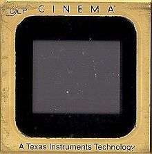
- Displays e.g., the digital micromirror device (DMD) chip in a projector based on DLP technology, which has a surface with several hundred thousand micromirrors or single micro-scanning-mirrors also called microscanners
- Optical switching technology, which is used for switching technology and alignment for data communications
- Bio-MEMS applications in medical and health related technologies from Lab-On-Chip to MicroTotalAnalysis (biosensor, chemosensor), or embedded in medical devices e.g. stents.[31]
- Interferometric modulator display (IMOD) applications in consumer electronics (primarily displays for mobile devices), used to create interferometric modulation − reflective display technology as found in mirasol displays
- Fluid acceleration such as for micro-cooling
- Micro-scale energy harvesting including piezoelectric,[32] electrostatic and electromagnetic micro harvesters.
- Micromachined ultrasound transducers.[33][34]
- MEMS-based loudspeakers focusing on applications such as in-ear headphones and hearing aids
Industry structure
The global market for micro-electromechanical systems, which includes products such as automobile airbag systems, display systems and inkjet cartridges totaled $40 billion in 2006 according to Global MEMS/Microsystems Markets and Opportunities, a research report from SEMI and Yole Development and is forecasted to reach $72 billion by 2011.[35]
Companies with strong MEMS programs come in many sizes. Larger firms specialize in manufacturing high volume inexpensive components or packaged solutions for end markets such as automobiles, biomedical, and electronics. Smaller firms provide value in innovative solutions and absorb the expense of custom fabrication with high sales margins. Both large and small companies typically invest in R&D to explore new MEMS technology.
The market for materials and equipment used to manufacture MEMS devices topped $1 billion worldwide in 2006. Materials demand is driven by substrates, making up over 70 percent of the market, packaging coatings and increasing use of chemical mechanical planarization (CMP). While MEMS manufacturing continues to be dominated by used semiconductor equipment, there is a migration to 200 mm lines and select new tools, including etch and bonding for certain MEMS applications.
See also
- Cantilever - one of the most common forms of MEMS
- Electrostatic motors used where coils are difficult to fabricate
- Electromechanical modeling
- Kelvin probe force microscope
- MEMS sensor generations
- MEMS thermal actuator, MEMS actuation created by thermal expansion
- Microoptoelectromechanical systems (MOEMS), MEMS including optical elements
- Microoptomechanical systems (MOMS), a class of MEMS which use optical and mechanical, but not electronic components
- Neural dust - millimeter-sized devices operated as wirelessly powered nerve sensors
- Photoelectrowetting, MEMS optical actuation using photo-sensitive wetting
- Micropower, Hydrogen generators, gas turbines, and electrical generators made of etched silicon
- Millipede memory, a MEMS technology for non-volatile data storage of more than a terabit per square inch
- Nanoelectromechanical systems are similar to MEMS but smaller
- Scratch drive actuator, MEMS actuation using repeatedly applied voltage differences
References
- Gabriel K, Jarvis J, Trimmer W (1988). Small Machines, Large Opportunities: A Report on the Emerging Field of Microdynamics: Report of the Workshop on Microelectromechanical Systems Research. National Science Foundation (sponsor). AT&T Bell Laboratories.
- Waldner JB (2008). Nanocomputers and Swarm Intelligence. London: ISTE John Wiley & Sons. p. 205. ISBN 9781848210097.
- Angell JB, Terry SC, Barth PW (1983). "Silicon Micromechanical Devices". Sci. Am. 248 (4): 44–55. Bibcode:1983SciAm.248d..44A. doi:10.1038/scientificamerican0483-44.
- Rai-Choudhury, P. (2000). MEMS and MOEMS Technology and Applications. SPIE Press. pp. ix, 3. ISBN 9780819437167.
- Nathanson HC, Wickstrom RA (1965). "A Resonant-Gate Silicon Surface Transistor with High-Q Band-Pass Properties". Appl. Phys. Lett. 7 (4): 84–86. Bibcode:1965ApPhL...7...84N. doi:10.1063/1.1754323.
- US patent 3614677A, Wilfinger RJ, "Electromechanical monolithic resonator", issued Oct 1971, assigned to International Business Machines Corp
- Wilfinger RJ, Bardell PH, Chhabra DS (1968). "The Resonistor: A Frequency Selective Device Utilizing the Mechanical Resonance of a Silicon Substrate". IBM J. Res. Dev. 12 (1): 113–8. doi:10.1147/rd.121.0113.
- Bergveld, Piet (October 1985). "The impact of MOSFET-based sensors" (PDF). Sensors and Actuators. 8 (2): 109–127. Bibcode:1985SeAc....8..109B. doi:10.1016/0250-6874(85)87009-8. ISSN 0250-6874.
- Beliveau, A.; Spencer, G.T.; Thomas, K.A.; Roberson, S.L. (1999-12-01). "Evaluation of MEMS capacitive accelerometers". IEEE Design & Test of Computers. 16 (4): 48–56. doi:10.1109/54.808209.
- "Introduction to MEMS and RF-MEMS: From the early days of microsystems to modern RF-MEMS passives". iop.org. 2017-11-01. Retrieved 2019-08-06.
- "MEMS technology is transforming high-density switch matrices". evaluationengineering.com. 2019-06-24. Retrieved 2019-08-06.
- Ghodssi R, Lin P (2011). MEMS Materials and Processes Handbook. Berlin: Springer. ISBN 9780387473161.
- M. Birkholz; K.-E. Ehwald; T. Basmer; et al. (2013). "Sensing glucose concentrations at GHz frequencies with a fully embedded Biomicro-electromechanical system (BioMEMS)". J. Appl. Phys. 113 (24): 244904–244904–8. Bibcode:2013JAP...113x4904B. doi:10.1063/1.4811351. PMC 3977869. PMID 25332510.
- Polster T, Hoffmann M (2009). "Aluminium nitride based 3D, piezoelectric, tactile sensors". Procedia Chemistry. 1 (1): 144–7. doi:10.1016/j.proche.2009.07.036.
- McCord MA, Rooks MJ (1997). "Electron Beam Lithography". In Choudhury PR (ed.). SPIE Handbook of Microlithography, Micromachining and Microfabrication. 1. London: SPIE. doi:10.1117/3.2265070.ch2. ISBN 9780819497864.
- Madou MJ (2011). From MEMS to Bio-MEMS and Bio-NEMS: Manufacturing Techniques and Applications. Fundamentals of Microfabrication and Nanotechnology. 3. Boca Raton: CRC Press. p. 252. ISBN 9781439895245.
- Williams KR, Muller RS (1996). "Etch rates for micromachining processing" (PDF). Journal of Microelectromechanical Systems. 5 (4): 256–269. CiteSeerX 10.1.1.120.3130. doi:10.1109/84.546406.
- Kovacs GT, Maluf NI, Petersen KE (1998). "Bulk micromachining of silicon" (PDF). Proc. IEEE. 86 (8): 1536–1551. doi:10.1109/5.704259. Archived from the original (PDF) on 27 Oct 2017.
- Chang FI, Yeh R, Lin G, et al. (1995). "Gas-phase silicon micromachining with xenon difluoride". In Bailey W, Motamedi ME, Luo F (eds.). Microelectronic Structures and Microelectromechanical Devices for Optical Processing and Multimedia Applications. 2641. Austin, TX: SPIE. p. 117. doi:10.1117/12.220933.
- Chang, Floy I-Jung (1995). Xenon difluoride etching of silicon for MEMS (M.S.). Los Angeles: University of California. OCLC 34531873.
- Brazzle JD, Dokmeci MR, Mastrangelo CH (2004). "Modeling and characterization of sacrificial polysilicon etching using vapor-phase xenon difluoride". 17th IEEE International Conference on Micro Electro Mechanical Systems. Maastricht MEMS 2004 Technical Digest. IEEE. pp. 737–740. doi:10.1109/MEMS.2004.1290690. ISBN 9780780382657.
- Laermer F, Urban A (2005). "Milestones in deep reactive ion etching". The 13th International Conference on Solid-State Sensors, Actuators and Microsystems, 2005. Digest of Technical Papers. TRANSDUCERS '05. 2. IEEE. pp. 1118–1121. doi:10.1109/SENSOR.2005.1497272. ISBN 9780780389946.
- Bustillo JM, Howe RT, Muller RS (1998). "Surface Micromachining for Microelectromechanical Systems" (PDF). Proc. IEEE. 86 (8): 1552–1574. CiteSeerX 10.1.1.120.4059. doi:10.1109/5.704260.
- Silicon-chip mid-infrared frequency comb generation Nature, 2015.
- Singh, Kulwant; Joyce, Robin; Varghese, Soney; Akhtar, J. (2015). "Fabrication of electron beam physical vapor deposited polysilicon piezoresistive MEMS pressure sensor". Sensors and Actuators A: Physical. 223: 151–158. doi:10.1016/j.sna.2014.12.033.
- Hosseinian E, Pierron ON (2013). "Quantitative in situ TEM tensile fatigue testing on nanocrystalline metallic ultrathin films". Nanoscale. 5 (24): 12532–41. Bibcode:2013Nanos...512532H. doi:10.1039/C3NR04035F. PMID 24173603.
- Acar C, Shkel AM (2008). MEMS Vibratory Gyroscopes: Structural Approaches to Improve Robustness. Springer Science. p. 111. ISBN 9780387095363.
- Johnson RC (2007). "There's more to MEMS than meets the iPhone". EE Times. Retrieved 14 Jun 2019.
- Clarke P (2016). "Smart MEMS microphones market emerges". EE News Analog. Retrieved 14 Jun 2019.
- "DS3231m RTC" (PDF). DS3231m RTC Datasheet. Maxim Inc. 2015. Retrieved 26 Mar 2019.
- Louizos LA, Athanasopoulos PG, Varty K (2012). "Microelectromechanical Systems and Nanotechnology. A Platform for the Next Stent Technological Era". Vasc. Endovasc. Surg. 46 (8): 605–609. doi:10.1177/1538574412462637. PMID 23047818.
- Hajati A, Kim SG (2011). "Ultra-wide bandwidth piezoelectric energy harvesting". Appl. Phys. Lett. 99 (8): 083105. Bibcode:2011ApPhL..99h3105H. doi:10.1063/1.3629551. hdl:1721.1/75264.
- Hajati A (2012). "Three-dimensional micro electromechanical system piezoelectric ultrasound transducer". Appl. Phys. Lett. 101 (25): 253101. Bibcode:2012ApPhL.101y3101H. doi:10.1063/1.4772469.
- Hajati A (2013). "Monolithic ultrasonic integrated circuits based on micromachined semi-ellipsoidal piezoelectric domes". Appl. Phys. Lett. 103 (20): 202906. Bibcode:2013ApPhL.103t2906H. doi:10.1063/1.4831988.
- "Worldwide MEMS Systems Market Forecasted to Reach $72 Billion by 2011". AZoNano. 2007. Retrieved 5 Oct 2015.
Further reading
- Journal of Micro and Nanotechnique
- Microsystem Technologies, published by Springer Publishing, Journal homepage
- Geschke, O.; Klank, H.; Telleman, P., eds. (2004). Microsystem Engineering of Lab-on-a-chip Devices. Wiley. ISBN 3-527-30733-8.
External links
| Wikimedia Commons has media related to MEMS. |
- Chollet, F.; Liu, HB. (10 August 2018). A (not so) short introduction to MEMS. ISBN 9782954201504. 5.4.