Die (integrated circuit)
A die, in the context of integrated circuits, is a small block of semiconducting material on which a given functional circuit is fabricated. Typically, integrated circuits are produced in large batches on a single wafer of electronic-grade silicon (EGS) or other semiconductor (such as GaAs) through processes such as photolithography. The wafer is cut ("diced") into many pieces, each containing one copy of the circuit. Each of these pieces is called a die.
To simplify handling and integration onto a printed circuit board, most dice are packaged in various forms.
There are three commonly used plural forms: "dice", "dies" and "die".[1][2]
Manufacturing process
An Integrated Circuit Die (ICD) is made up of different elements, including sand and silicon [3]. All the elements are combined to create a Mono-crystal Silicon Ingot. These ingots are then sliced into disks with a diameter of ~300mm. These wafers are then polished to a mirror finish before going through photolithography. The prepared wafers are then washed and go through ion implantation. They then go through an electroplating process involving copper, which creates the physical transistors within the die. The excess copper is then washed off to make way for the many metal layers. The metal layers are used to connect the various transistors within the die to each other, allowing them to make one coherent processing unit. These prepared wafers then go through wafer testing to test their functionality. The wafers are then sliced and sorted to filter out the faulty dies. The remaining dies are then placed on a substrate and are usually topped with a heat spreader. Once this process is complete, the completed die is ready to be shipped.
Uses
An ICD can be integrated into many different use cases. The most common use case of an ICD is in the form of a Central Processing Unit (CPU). Through advances in modern technology, the size of the transistor within the die has shrunk exponentially, following Moore's Law. Other uses for ICDs can range from light fixtures to complex multi-core processing operations.
Images
 Single NPN bipolar junction transistor die.
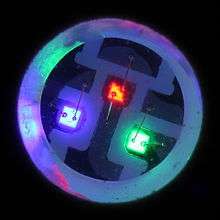 Close-up of an RGB light-emitting diode, showing the three individual dice.
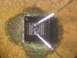
 A small-scale integrated circuit die, with bond wires attached.
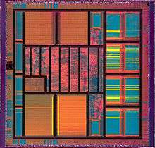 A VLSI integrated-circuit die.
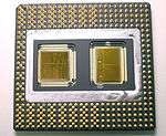 Two dice bonded onto one chip carrier.
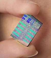 The "naked" die without chip carrier of a Cell processor.
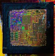
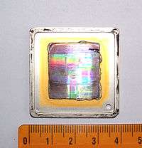 Intel Xeon E7440 die, mounted on heat spreader. Die is 22×23 mm (506 mm2), and contains 1900000000 transistors.
See also
References
- ↑ John E. Ayers (2004). Digital Integrated Circuits. CRC Press. ISBN 0-8493-1951-X. Archived from the original on 2017-01-31.
- ↑ Robert Allen Meyers (2000). Encyclopedia of Physical Science and Technology. Academic Press. ISBN 0-12-226930-6. Archived from the original on 2017-01-31.
- ↑ From Sand to Silicon “Making of a Chip” Illustrations. (n.d.). Retrieved from http://download.intel.com/pressroom/kits/chipmaking/Making_of_a_Chip.pdf
External links
- Wedge Bonding Process on YouTube – animation
- Industrial Bonder on YouTube – the video shows bonding not brazing
| Wikimedia Commons has media related to Integrated circuit dies. |