Insulated-gate bipolar transistor
An insulated-gate bipolar transistor (IGBT) is a three-terminal power semiconductor device primarily used as an electronic switch which, as it was developed, came to combine high efficiency and fast switching. It consists of four alternating layers (P-N-P-N) that are controlled by a metal-oxide-semiconductor (MOS) gate structure without regenerative action. Although the structure of the IGBT is topologically the same as a thyristor with a MOS gate (MOS gate thyristor), the thyristor action is completely suppressed and only the transistor action is permitted in the entire device operation range. It switches electric power in many applications: variable-frequency drives (VFDs), electric cars, trains, variable speed refrigerators, lamp ballasts, air-conditioners and even stereo systems with switching amplifiers.
Since it is designed to turn on and off rapidly, amplifiers that use it often synthesize complex waveforms with pulse-width modulation and low-pass filters. In switching applications modern devices feature pulse repetition rates well into the ultrasonic range—frequencies which are at least ten times the highest audio frequency handled by the device when used as an analog audio amplifier.
| IGBT Comparison Table [1] | |||
|---|---|---|---|
| Device Characteristic | Power Bipolar | Power MOSFET | IGBT |
| Voltage Rating | High <1kV | High <1kV | Very High >1kV |
| Current Rating | High <500A | High > 500A | High >500A |
| Input Drive | Current ratio hFE 20-200 |
Voltage VGS 3-10V |
Voltage VGE 4-8V |
| Input Impedance | Low | High | High |
| Output Impedance | Low | Medium | Low |
| Switching Speed | Slow (µs) | Fast (ns) | Medium |
| Cost | Low | Medium | High |
Device structure
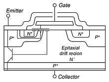
An IGBT cell is constructed similarly to a n-channel vertical-construction power MOSFET, except the n+ drain is replaced with a p+ collector layer, thus forming a vertical PNP bipolar junction transistor. This additional p+ region creates a cascade connection of a PNP bipolar junction transistor with the surface n-channel MOSFET.
History
The first-generation IGBTs of the 1980s and early 1990s were prone to failure through effects such as latchup (in which the device will not turn off as long as current is flowing) and secondary breakdown (in which a localized hotspot in the device goes into thermal runaway and burns the device out at high currents). Second-generation devices were much improved. The current third-generation IGBTs are even better, with speed rivaling MOSFETs, and excellent ruggedness and tolerance of overloads.[2] Extremely high pulse ratings of second and third-generation devices also make them useful for generating large power pulses in areas including particle and plasma physics, where they are starting to supersede older devices such as thyratrons and triggered spark gaps. High pulse ratings and low prices on the surplus market also make them attractive to the high-voltage hobbyists for controlling large amounts of power to drive devices such as solid-state Tesla coils and coilguns.
IGBT mode of operation was first proposed by Yamagami in his Japanese patent S47-21739, which was filed in 1968. This mode of operation was first experimentally reported in the lateral four-layer device (SCR) by B. W. Scharf and J. D. Plummer in 1978.[3] This mode of operation was also experimentally discovered in vertical device in 1979 by B. Jayant Baliga.[4] The device structure was referred to as a "V-groove MOSFET device with the drain region replaced by a p-type anode region" in this paper and subsequently as "the insulated-gate rectifier" (IGR),[5] the insulated-gate transistor (IGT),[6] the conductivity-modulated field-effect transistor (COMFET)[7] and "bipolar-mode MOSFET".[8]
Plummer filed a patent application for IGBT mode of operation in the four-layer device (SCR) in 1978. USP No. 4199774 was issued in 1980, and B1 Re33209[9] was reissued in 1995 for the IGBT mode operation in the four-layer device (SCR).
The IGBT mode of operation in the four-layer device (SCR) switched to thyristor operation if the collector current exceeded the latch-up current, which is called as "holding current" in the well known theory of the thyristor. The development of IGBT was characterized by the efforts to completely suppress the thyristor operation or the latch-up in the four-layer device because the latch-up caused the fatal device failure. The technology of IGBT had, thus, been established when the complete suppression of the latch-up of the parasitic thyristor was achieved as described in the following.
Hans W. Becke and Carl F. Wheatley invented a similar device, for which they filed a patent application in 1980, and which they referred to as "power MOSFET with an anode region".[10] This patent has been called "the seminal patent of the insulated gate bipolar transistor".[11] The patent claimed that "no thyristor action occurs under any device operating conditions". This substantially means that the device exhibits non-latch-up IGBT operation over the entire device operation range.
A. Nakagawa et. al. invented the device design concept of non-latch-up IGBTs in 1984.[12] The invention[13] is characterized by the device design setting the device saturation current below the latch-up current, which triggers the parasitic thyristor. This invention realized complete suppression of the parasitic thyristor action, for the first time, because the maximal collector current was limited by the saturation current and never exceeded the latch-up current. After the invention of the device design concept of non-latch-up IGBTs, IGBTs evolved rapidly, and the design of non-latch-up IGBTs became a de facto standard and the patent of non-latch-up IGBTs became the basic IGBT patent of actual devices.
There are two important device concepts concerning IGBTs. First one is the device concept discovered by J. D. Plummer in 1978. US Patent Re.33209 was issued for the device concept. The device proposed by J. D. Plummer is the same structure as a thyristor with a MOS gate. J. D. Plummer discovered and proposed that the device can be used as a transistor although the device operates as a thyristor in higher current density level. J. D. Plummer reported this fact in his technical paper: "A MOS-Controlled Triac Devices" B.W. Scharf and J.D. Plummer, 1978 IEEE International Solid-State Circuits Conference, SESSION XVI FAM 16.6.[14] The device proposed by J. D. Plummer is referred, here, as “Plummer’s device.” On the other hand, Hans W. Becke invented and proposed, in 1980, another new device in which the thyristor action is completely eliminated under any device operating conditions although the basic device structure is the same as that proposed by J. D. Plummer. The device invented by Hans W. Becke is referred, here, as “Becke’s device” and is described in US Patent 4364073. The difference between “Plummer’s device” and “Becke’s device” is that “Plummer’s device” has the mode of thyristor action in its operation range and “Becke’s device” never has the mode of thyristor action in its entire operation range. This is a critical point, because the thyristor action is the same as so-called “latch-up.” “Latch-up” is the main cause of fatal device failure. Thus, theoretically, “Plummer’s device” never realizes a rugged or strong power device which has a large safe operating area. The large safe operating area can be achieved only after “latch-up” is completely suppressed and eliminated in the entire device operation range. Hence, the invention of the device by Hans W. Becke is decisively more important. And, this is the real IGBT. However, the Becke's patent (US Patent 4364073) did not disclose any measures to realize actual devices.
In the early development stage of IGBT, all the researchers tried to increase the latch-up current itself in order to suppress the latch-up of the parasitic thyristor. However, all these efforts failed because IGBT could conduct enormously large current. Successful suppression of the latch-up was made possible by limiting the maximal collector current, which IGBT could conduct, below the latch-up current by controlling/reducing the saturation current of the inherent MOSFET. This was the concept of non-latch-up IGBT. “Becke’s device” was made possible by the non-latch-up IGBT.
The IGBT is characterized by its ability to simultaneously handle a high voltage and a large current. The product of the voltage and the current density that the IGBT can handle reached more than 5×10⁵ W/cm2,[2][15] which far exceeded the value, 2×10⁵ W/cm2, of existing power devices such as bipolar transistors and power MOSFETs. This is a consequence of the large safe operating area of the IGBT. The IGBT is the most rugged and the strongest power device that ever developed, thus, providing users with easy use of the device and displaced bipolar transistors and even GTOs. This excellent feature of the IGBT had suddenly emerged when the non-latch-up IGBT was established in 1984 by solving the problem of so-called “latch-up,” which is the main cause of device destruction or device failure. Before that, the developed devices were very weak and were easy to be destroyed because of “latch-up.”
IGBT is defined as a transistor. Thus, the device, which operates in IGBT-mode and switches to thyristor operation in higher current, should not be called as IGBT. Thus, the invention of Plummer, USP No. 419977, Re33209, which is cited above, is not IGBT. MOS gate thyristor is not IGBT, either. Even "IGT" is not actual IGBT, because the switching safe operation area is narrow and limited by latch-up and because the allowable maximal collector current could not be turned-off due to thyristor action of "latch-up." The detailed discussions will be necessary.
Patent issues in the development of IGBT
IGBT manufacturers paid the license fee of Becke’s patent.[10] Toshiba commercialized “non-latch-up IGBT” in 1985. Stanford University insisted in 1991 that Toshiba’s device infringed US Patent Re. 33209 of “Plummer’s device.” Toshiba answered that “non-latch-up IGBTs” never latched up in the entire device operation range, thus did not infringe US Patent Re. 33209 of “Plummer’s patent.” Stanford University never responded after Nov. 1992. Toshiba purchased the license of “Becke’s patent.” Toshiba never paid any license fee of “Plummer’s device.” Other IGBT manufacturers also paid the license fee of Becke’s patent.
Practical devices
Practical devices capable of operating over an extended current range were first reported by Baliga et al. in 1982.[5] A similar paper was also submitted by J. P. Russel et al. to IEEE Electron Device Letter in 1982.[7] The applications for the device were initially regarded by the power electronics community to be severely restricted by its slow switching speed and latch-up of the parasitic thyristor structure inherent within the device. However, it was demonstrated by Baliga and also by A. M. Goodman et al. in 1983 that the switching speed could be adjusted over a broad range by using electron irradiation.[6][16] This was followed by demonstration of operation of the device at elevated temperatures by Baliga in 1985.[17] Successful efforts to suppress the latch-up of the parasitic thyristor and the scaling of the voltage rating of the devices at GE allowed the introduction of commercial devices in 1983,[18] which could be utilized for a wide variety of applications. The electrical characteristics of GE's device, IGT D94FQ/FR4, were reported in detail by Marvin W. Smith in the proceedings of PCI April 1984.[19] Marvin W. Smith showed in Fig.12 of the proceedings that turn-off above 10 amperes for gate resistance of 5kOhm and above 5 amperes for gate resistance of 1kOhm was limited by switching safe operating area although IGT D94FQ/FR4 was able to conduct 40 amperes of collector current. Marvin W. Smith also stated that the switching safe operating area was limited by the latch-up of the parasitic thyristor.
Complete suppression of the parasitic thyristor action and the resultant non-latch-up IGBT operation for the entire device operation range was achieved by A. Nakagawa et al. in 1984.[20] The non-latch-up design concept was filed for US patents.[21] To test the lack of latch-up, the prototype 1200V IGBTs were directly connected without any loads across a 600V constant voltage source and were switched on for 25 microseconds. The entire 600V was dropped across the device and a large short circuit current flowed. The devices successfully withstood this severe condition. This was the first demonstration of so-called "short-circuit-withstanding-capability" in IGBTs. Non-latch-up IGBT operation was ensured, for the first time, for the entire device operation range.[15] In this sense, the non-latch-up IGBT proposed by Hans W. Becke and Carl F. Wheatley was realized by A. Nakagawa et al. in 1984. Products of non-latch-up IGBTs were first commercialized by Toshiba in 1985. This was the real birth of the present IGBT.
Once the non-latch-up capability was achieved in IGBTs, it was found that IGBTs exhibited very rugged and a very large safe operating area. It was demonstrated that the product of the operating current density and the collector voltage exceeded the theoretical limit of bipolar transistors, 2×10⁵ W/cm2, and reached 5×10⁵ W/cm2.[2][15]
The insulating material is typically made of solid polymers which have issues with degradation. There are developments that use an ion gel to improve manufacturing and reduce the voltage required.[22]
Applications and advantages
The IGBT combines the simple gate-drive characteristics of MOSFETs with the high-current and low-saturation-voltage capability of bipolar transistors. The IGBT combines an isolated-gate FET for the control input and a bipolar power transistor as a switch in a single device. The IGBT is used in medium- to high-power applications like switched-mode power supplies, traction motor control and induction heating. Large IGBT modules typically consist of many devices in parallel and can have very high current-handling capabilities in the order of hundreds of amperes with blocking voltages of 6500 V. These IGBTs can control loads of hundreds of kilowatts.
Comparison with power MOSFETs
An IGBT features a significantly lower forward voltage drop compared to a conventional MOSFET in higher blocking voltage rated devices, although, MOSFETS exhibit much lower forward voltage at lower current densities due to the absence of a diode Vf in the IGBT's output BJT. As the blocking voltage rating of both MOSFET and IGBT devices increases, the depth of the n- drift region must increase and the doping must decrease, resulting in roughly square relationship decrease in forward conduction versus blocking voltage capability of the device. By injecting minority carriers (holes) from the collector p+ region into the n- drift region during forward conduction, the resistance of the n- drift region is considerably reduced. However, this resultant reduction in on-state forward voltage comes with several penalties:
- The additional PN junction blocks reverse current flow. This means that unlike a MOSFET, IGBTs cannot conduct in the reverse direction. In bridge circuits, where reverse current flow is needed, an additional diode (called a freewheeling diode) is placed in parallel (actually anti-parallel) with the IGBT to conduct current in the opposite direction. The penalty isn't overly severe because at higher voltages, where IGBT usage dominates, discrete diodes have a significantly higher performance than the body diode of a MOSFET.
- The reverse bias rating of the N-drift region to collector P+ diode is usually only of tens of volts, so if the circuit application applies a reverse voltage to the IGBT, an additional series diode must be used.
- The minority carriers injected into the N-drift region take time to enter and exit or recombine at turn-on and turn-off. This results in longer switching times, and hence higher switching loss compared to a power MOSFET.
- The on-state forward voltage drop in IGBTs behaves very differently from power MOSFETS. The MOSFET voltage drop can be modeled as a resistance, with the voltage drop proportional to current. By contrast, the IGBT has a diode-like voltage drop (typically of the order of 2V) increasing only with the log of the current. Additionally, MOSFET resistance is typically lower for smaller blocking voltages, so the choice between IGBTs and power MOSFETS will depend on both the blocking voltage and current involved in a particular application.
In general, high voltage, high current and low switching frequencies favor the IGBT while low voltage, low current and high switching frequencies are the domain of the MOSFET.
IGBT models
Circuits with IGBTs can be developed and modeled with various circuit simulating computer programs such as SPICE, Saber, and other programs. To simulate an IGBT circuit, the device (and other devices in the circuit) must have a model which predicts or simulates the device's response to various voltages and currents on their electrical terminals. For more precise simulations the effect of temperature on various parts of the IGBT may be included with the simulation. Two common methods of modeling are available: device physics-based model, equivalent circuits or macromodels. SPICE simulates IGBTs using a macromodel that combines an ensemble of components like FETs and BJTs in a Darlington configuration. An alternative physics-based model is the Hefner model, introduced by Allen Hefner of the National Institute of Standards and Technology. Hefner's model is fairly complex that has shown very good results. Hefner's model is described in a 1988 paper and was later extended to a thermo-electrical model which include the IGBT's response to internal heating. This model has been added to a version of the Saber simulation software.[23]
Usage
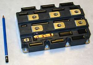 IGBT-Module (IGBTs and freewheeling diodes) with a rated current of 1,200 A and a maximum voltage of 3,300 V | 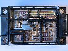 | 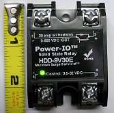 Small IGBT module, rated up to 30 A, up to 900 V | 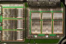 Mitsubishi Electric CM600DU-24NFH IGBT module rated for 600 A 1200 V, with the cover removed to show the IGBT dies and freewheeling diodes. |
See also
References
- ↑ Basic Electronics Tutorials.
- 1 2 3 A. Nakagawa et al., "Safe operating area for 1200-V non-latch-up bipolar-mode MOSFETs", IEEE Trans. on Electron Devices, ED-34, pp. 351–355 (1987).
- ↑ B. W. Scharf and J. D. Plummer, 1978 IEEE International Solid-State Circuits Conference, SESSION XVI FAM 16.6 "A MOS-Controlled Triac Devices".
- ↑ B. J. Baliga, "ENHANCEMENT- AND DEPLETION-MODE VERTICAL-CHANNEL M.O.S. GATED THYRISTORS" Electronics Letters p. 645 (1979).
- 1 2 B. J. Baliga, et al., "The insulated gate rectifier (IGR): A new power switching device", IEEE International Electron Devices Meeting, Abstract 10.6, pp. 264–267 (1982).
- 1 2 B. J. Baliga, "Fast-switching insulated gate transistors", IEEE Electron Device Letters, Vol. EDL-4, pp. 452–454 (1983).
- 1 2 J.P. Russel et al., "The COMFET—A new high conductance MOS-gated device", IEEE Electron Device Lett., vol. EDL-4, pp. 63–65, 1983
- ↑ A. Nakagawa et al., "High voltage bipolar-mode MOSFETs with high current capability", Ext. Abst. of SSDM, pp. 309–312 (1984).
- ↑ B1 Re33209 is attached in the pdf file of Re 33209.
- 1 2 U. S. Patent No. 4,364,073, Power MOSFET with an Anode Region, issued December 14, 1982 to Hans W. Becke and Carl F. Wheatley.
- ↑ "C. Frank Wheatley, Jr., BSEE". Innovation Hall of Fame at A. James Clark School of Engineering.
- ↑ A. Nakagawa et al., "Non-latch-up 1200V 75A bipolar-mode MOSFET with large ASO", IEEE International Electron Devices Meeting Technical Digest, pp. 860–861 (1984).
- ↑ A. Nakagawa, H. Ohashi, Y. Yamaguchi, K. Watanabe and T. Thukakoshi, "Conductivity modulated MOSFET" US Patent No. 6025622 (Feb. 15, 2000), No. 5086323 (Feb. 4, 1992) and No. 4672407 (Jun. 9, 1987).
- ↑ "A MOS-Controlled Triac Devices" B.W. Scharf and J.D. Plummer, 1978 IEEE International Solid-State Circuits Conference, SESSION XVI FAM 16.6
- 1 2 3 A. Nakagawa et al., "Experimental and numerical study of non-latch-up bipolar-mode MOSFET characteristics", IEEE International Electron Devices Meeting Technical Digest, pp. 150–153, 1985
- ↑ A. M. Goodman et al., "Improved COMFETs with fast switching speed and high-current capability", IEEE International Electron Devices Meeting Technical Digest, pp. 79–82,1983
- ↑ B. J. Baliga, "Temperature behavior of insulated gate transistor characteristics", Solid State Electronics, Vol. 28, pp. 289–297, 1985.
- ↑ Product of the Year Award: "Insulated Gate Transistor", General Electric Company, Electronics Products, 1983.
- ↑ Marvin W. Smith, "APPLICATIONS OF INSULATED GATE TRANSISTORS" PCI April 1984 PROCEEDINGS, pp. 121-131, 1984
- ↑ A. Nakagawa et al., "Non-latch-up 1200V 75A bipolar-mode MOSFET with large ASO", IEEE International Electron Devices Meeting Technical Digest, pp.860-861,1984.
- ↑ A.Nakagawa, H. Ohashi, Y. Yamaguchi, K. Watanabe and T. Thukakoshi, "Conductivity modulated MOSFET" US Patent No.6025622(Feb.15, 2000), No.5086323 (Feb.4, 1992) and No.4672407(Jun.9, 1987)
- ↑ "Ion Gel as a Gate Insulator in Field Effect Transistors". Archived from the original on 2011-11-14.
- ↑ Hefner Jr., Allen R Jr; Diebolt, DM (1994). "An experimentally verified IGBT model implemented in the Saber circuit simulator". 9 (5). IEEE Transactions on Power Electronics: 532–542. Retrieved January 2016. Check date values in:
|accessdate=(help)
Further reading
- Wintrich, Arendt; Nicolai, Ulrich; Tursky, Werner; Reimann, Tobias (2015). Application Manual Power Semiconductors (PDF-Version) (2nd Revised ed.). Germany: ISLE Verlag. ISBN 978-3-938843-83-3.
External links
| Wikimedia Commons has media related to IGBT. |