Surface-mount technology
Surface-mount technology (SMT) is a method in which the electrical components are mounted directly onto the surface of a printed circuit board (PCB). An electrical component mounted in this manner is referred to as a surface-mount device (SMD). In industry, this approach has largely replaced the through-hole technology construction method of fitting components, in large part because SMT allows for increased manufacturing automation. Both technologies can be used on the same board, with the through-hole technology often used for components not suitable for surface mounting such as large transformers and heat-sinked power semiconductors.
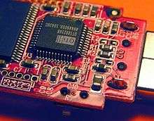
An SMT component is usually smaller than its through-hole counterpart because it has either smaller leads or no leads at all. It may have short pins or leads of various styles, flat contacts, a matrix of solder balls (BGAs), or terminations on the body of the component.
History
Surface mounting was originally called "planar mounting".[1]
Surface-mount technology was developed in the 1960s and became widely used in the mid 1980s. By the late 1990s, the great majority of high-tech electronic printed circuit assemblies were dominated by surface mount devices. Much of the pioneering work in this technology was done by IBM. The design approach first demonstrated by IBM in 1960 in a small-scale computer was later applied in the Launch Vehicle Digital Computer used in the Instrument Unit that guided all Saturn IB and Saturn V vehicles.[2] Components were mechanically redesigned to have small metal tabs or end caps that could be directly soldered to the surface of the PCB. Components became much smaller and component placement on both sides of a board became far more common with surface mounting than through-hole mounting, allowing much higher circuit densities and smaller circuit boards and, in turn, machines or subassemblies containing the boards.
Often only the solder joints hold the parts to the board; in rare cases parts on the bottom or "second" side of the board may be secured with a dot of adhesive to keep components from dropping off inside reflow ovens if the part has a large size or weight. Adhesive is sometimes used to hold SMT components on the bottom side of a board if a wave soldering process is used to solder both SMT and through-hole components simultaneously. Alternatively, SMT and through-hole components can be soldered on the same side of a board without adhesive if the SMT parts are first reflow-soldered, then a selective solder mask is used to prevent the solder holding those parts in place from reflowing and the parts floating away during wave soldering. Surface mounting lends itself well to a high degree of automation, reducing labor cost and greatly increasing production rates.
Conversely, SMT does not lend itself well to manual or low-automation fabrication, which is more economical and faster for one-off prototyping and small-scale production, and this is one reason why many through-hole components are still manufactured. Some SMDs can be soldered with a temperature-controlled manual soldering iron, but unfortunately, those that are very small or have too fine a lead pitch are impossible to manually solder without expensive hot-air solder reflow equipment. SMDs can be one-quarter to one-tenth the size and weight, and one-half to one-quarter the cost of equivalent through-hole parts, but on the other hand, the costs of a certain SMT part and of an equivalent through-hole part may be quite similar, though rarely is the SMT part more expensive.
Common abbreviations
Different terms describe the components, technique, and machines used in manufacturing. These terms are listed in the following table:
| SMp term | Expanded form |
|---|---|
| SMD | Surface-mount devices (active, passive and electromechanical components) |
| SMT | Surface-mount technology (assembling and mounting technology) |
| SMA | Surface-mount assembly (module assembled with SMT) |
| SMC | Surface-mount components (components for SMT) |
| SMP | Surface-mount packages (SMD case forms) |
| SME | Surface-mount equipment (SMT assembling machines) |
Assembly techniques
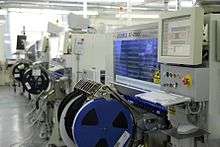
Where components are to be placed, the printed circuit board normally has flat, usually tin-lead, silver, or gold plated copper pads without holes, called solder pads. Solder paste, a sticky mixture of flux and tiny solder particles, is first applied to all the solder pads with a stainless steel or nickel stencil using a screen printing process. It can also be applied by a jet-printing mechanism, similar to an inkjet printer. After pasting, the boards then proceed to the pick-and-place machines, where they are placed on a conveyor belt. The components to be placed on the boards are usually delivered to the production line in either paper/plastic tapes wound on reels or plastic tubes. Some large integrated circuits are delivered in static-free trays. Numerical control pick-and-place machines remove the parts from the tapes, tubes or trays and place them on the PCB.[3]
The boards are then conveyed into the reflow soldering oven. They first enter a pre-heat zone, where the temperature of the board and all the components is gradually, uniformly raised. The boards then enter a zone where the temperature is high enough to melt the solder particles in the solder paste, bonding the component leads to the pads on the circuit board. The surface tension of the molten solder helps keep the components in place, and if the solder pad geometries are correctly designed, surface tension automatically aligns the components on their pads.
There are a number of techniques for reflowing solder. One is to use infrared lamps; this is called infrared reflow. Another is to use a hot gas convection. Another technology which is becoming popular again is special fluorocarbon liquids with high boiling points which use a method called vapor phase reflow. Due to environmental concerns, this method was falling out of favor until lead-free legislation was introduced which requires tighter controls on soldering. At the end of 2008, convection soldering was the most popular reflow technology using either standard air or nitrogen gas. Each method has its advantages and disadvantages. With infrared reflow, the board designer must lay the board out so that short components don't fall into the shadows of tall components. Component location is less restricted if the designer knows that vapor phase reflow or convection soldering will be used in production. Following reflow soldering, certain irregular or heat-sensitive components may be installed and soldered by hand, or in large-scale automation, by focused infrared beam (FIB) or localized convection equipment.
If the circuit board is double-sided then this printing, placement, reflow process may be repeated using either solder paste or glue to hold the components in place. If a wave soldering process is used, then the parts must be glued to the board prior to processing to prevent them from floating off when the solder paste holding them in place is melted.
After soldering, the boards may be washed to remove flux residues and any stray solder balls that could short out closely spaced component leads. Rosin flux is removed with fluorocarbon solvents, high flash point hydrocarbon solvents, or low flash solvents e.g. limonene (derived from orange peels) which require extra rinsing or drying cycles. Water-soluble fluxes are removed with deionized water and detergent, followed by an air blast to quickly remove residual water. However, most electronic assemblies are made using a "No-Clean" process where the flux residues are designed to be left on the circuit board, since they are considered harmless. This saves the cost of cleaning, speeds up the manufacturing process, and reduces waste. However, it is generally suggested to wash the assembly, even when a "No-Clean" process is used, when the application uses very high frequency clock signals (in excess of 1 GHz). Another reason to remove no-clean residues is to improve adhesion of conformal coatings and underfill materials.[4] Regardless of cleaning or not those PCBs, current industry trend suggests to carefully review a PCB assembly process where "No-Clean" is applied, since flux residues trapped under components and RF shields may affect surface insulation resistance (SIR), especially on high component density boards.[5]
Certain manufacturing standards, such as those written by the IPC - Association Connecting Electronics Industries require cleaning regardless of the solder flux type used to ensure a thoroughly clean board. Proper cleaning removes all traces of solder flux, as well as dirt and other contaminants that may be invisible to the naked eye. No-Clean or other soldering processes may leave "white residues" that, according to IPC, are acceptable "provided that these residues have been qualified and documented as benign".[6] However, while shops conforming to IPC standard are expected to adhere to the Association's rules on board condition, not all manufacturing facilities apply IPC standard, nor are they required to do so. Additionally, in some applications, such as low-end electronics, such stringent manufacturing methods are excessive both in expense and time required.
Finally, the boards are visually inspected for missing or misaligned components and solder bridging. If needed, they are sent to a rework station where a human operator repairs any errors. They are then usually sent to the testing stations (in-circuit testing and/or functional testing) to verify that they operate correctly.
Automated optical inspection (AOI) systems are commonly used in PCB manufacturing. This technology has proven highly efficient for process improvements and quality achievements.[7]
Advantages
The main advantages of SMT over the older through-hole technique are:
- Smaller components.
- Much higher component density (components per unit area) and many more connections per component.
- Components can be placed on both sides of the circuit board.
- Higher density of connections because holes do not block routing space on inner layers, nor on back-side layers if components are mounted on only one side of the PCB.
- Small errors in component placement are corrected automatically as the surface tension of molten solder pulls components into alignment with solder pads. (On the other hand, through-hole components cannot be slightly misaligned, because once the leads are through the holes, the components are fully aligned and cannot move laterally out of alignment.)
- Better mechanical performance under shock and vibration conditions (partly due to lower mass, and partly due to less cantilevering)
- Lower resistance and inductance at the connection; consequently, fewer unwanted RF signal effects and better and more predictable high-frequency performance.
- Better EMC performance (lower radiated emissions) due to the smaller radiation loop area (because of the smaller package) and the lesser lead inductance.[8]
- Fewer holes need to be drilled. (Drilling PCBs is time-consuming and expensive.)
- Lower initial cost and time of setting up for mass production, using automated equipment.
- Simpler and faster automated assembly. Some placement machines are capable of placing more than 136,000 components per hour.
- Many SMT parts cost less than equivalent through-hole parts.
- A surface mount package is favored where a low profile package is required or the space available to mount the package is limited. As electronic devices become more complex and available space is reduced, the desirability of a surface mount package increases. Concurrently, as the device complexity increases, the heat generated by operation increases. If the heat is not removed, the temperature of the device rises shortening the operational life. It is therefore highly desirable to develop surface mount packages having high thermal conductivity.[9]
Disadvantages
- SMT may be unsuitable as the sole attachment method for components that are subject to frequent mechanical stress, such as connectors that are used to interface with external devices that are frequently attached and detached.
- SMDs' solder connections may be damaged by potting compounds going through thermal cycling.
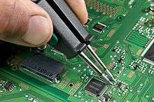
- Manual prototype assembly or component-level repair is more difficult and requires skilled operators and more expensive tools, due to the small sizes and lead spacings of many SMDs.[10] Handling of small SMT components can be difficult, requiring tweezers, unlike nearly all through-hole components. Whereas through-hole components will stay in place (under gravitational force) once inserted and can be mechanically secured prior to soldering by bending out two leads on the solder side of the board, SMDs are easily moved out of place by a touch of a soldering iron. Without developed skill, when manually soldering or desoldering a component, it is easy to accidentally reflow the solder of an adjacent SMT component and unintentionally displace it, something that is almost impossible to do with through-hole components.
- Many types of SMT component packages cannot be installed in sockets, which provide for easy installation or exchange of components to modify a circuit and easy replacement of failed components. (Virtually all through-hole components can be socketed.)
- SMDs cannot be used directly with plug-in breadboards (a quick snap-and-play prototyping tool), requiring either a custom PCB for every prototype or the mounting of the SMD upon a pin-leaded carrier. For prototyping around a specific SMD component, a less-expensive breakout board may be used. Additionally, stripboard style protoboards can be used, some of which include pads for standard sized SMD components. For prototyping, "dead bug" breadboarding can be used.[11]
- Solder joint dimensions in SMT quickly become much smaller as advances are made toward ultra-fine pitch technology. The reliability of solder joints becomes more of a concern, as less and less solder is allowed for each joint. Voiding is a fault commonly associated with solder joints, especially when reflowing a solder paste in the SMT application. The presence of voids can deteriorate the joint strength and eventually lead to joint failure.[12][13]
- SMDs, usually being smaller than equivalent through-hole components, have less surface area for marking, requiring marked part ID codes or component values to be more cryptic and smaller, often requiring magnification to be read, whereas a larger through-hole component could be read and identified by the unaided eye. This is a disadvantage for prototyping, repair, rework, reverse engineering, and possibly for production set-up.
Rework
Defective surface-mount components can be repaired by using soldering irons (for some connections), or using a non-contact rework system. In most cases a rework system is the better choice because SMD work with a soldering iron requires considerable skill and is not always feasible.
Reworking usually corrects some type of error, either human- or machine-generated, and includes the following steps:
- Melt solder and remove component(s)
- Remove residual solder
- Print solder paste on PCB, directly or by dispensing
- Place new component and reflow.
Sometimes hundreds or thousands of the same part need to be repaired. Such errors, if due to assembly, are often caught during the process. However, a whole new level of rework arises when component failure is discovered too late, and perhaps unnoticed until the end user of the device being manufactured experiences it. Rework can also be used if products of sufficient value to justify it require revision or re-engineering, perhaps to change a single firmware-based component. Reworking in large volume requires an operation designed for that purpose.
There are essentially two non-contact soldering/desoldering methods: infrared soldering and soldering with hot gas.[14]
Infrared
With infrared soldering, the energy for heating up the solder joint is transmitted by long- or short-wave infrared electromagnetic radiation.
Advantages:
- Easy setup
- No compressed air required
- No requirement for different nozzles for many component shapes and sizes, reducing cost and the need to change nozzles
- Fast reaction of infrared source (depends on system used)
Disadvantages:
- Central areas will be heated more than peripheral areas
- Temperature control is less precise, and there may be peaks
- Nearby components must be shielded from heat to prevent damage, which requires additional time for every board
- Surface temperature depends on the component's albedo: dark surfaces will be heated more than lighter surfaces
- The temperature additionally depends on the surface shape. Convective loss of energy will reduce the temperature of the component
- No reflow atmosphere possible
Hot gas
During hot gas soldering, the energy for heating up the solder joint is transmitted by a hot gas. This can be air or inert gas (nitrogen).
Advantages:
- Simulating reflow oven atmosphere
- Some systems allow switching between hot air and nitrogen
- Standard and component-specific nozzles allow high reliability and faster processing
- Allow reproducible soldering profiles
- Efficient heating, large amounts of heat can be transferred
- Even heating of the affected board area
- Temperature of the component will never exceed the adjusted gas temperature
- Rapid cooling after reflow, resulting in small-grained solder joints (depends on system used)
Disadvantages:
- Thermal capacity of the heat generator results in slow reaction whereby thermal profiles can be distorted (depends on system used)
Packages
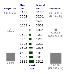
Surface-mount components are usually smaller than their counterparts with leads, and are designed to be handled by machines rather than by humans. The electronics industry has standardized package shapes and sizes (the leading standardisation body is JEDEC).
Identification
- Resistors
- For 5% precision SMD resistors usually are marked with their resistance values using three digits: two significant digits and a multiplier digit. These are quite often white lettering on a black background, but other colored backgrounds and lettering can be used. The black or colored coating is usually only on one face of the device, the sides and other face simply being the uncoated, usually white ceramic substrate. The coated surface, with the resistive element beneath is normally positioned face up when the device is soldered to the board, although they can be seen in rare cases mounted with the uncoated underside face up, whereby the resistance value code is not visible. For 1% precision SMD resistors, the code is used, as three digits would otherwise not convey enough information. This code consists of two digits and a letter: the digits denote the value's position in the E96 sequence, while the letter indicates the multiplier.[15]
- Capacitors
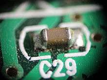
- Non-electrolytic capacitors are usually unmarked and the only reliable method of determining their value is removal from the circuit and subsequent measurement with a capacitance meter or impedance bridge. The materials used to fabricate the capacitors, such as nickel tantalate, possess different colours and these can give an approximate idea of the capacitance of the component. Generally physical size is proportional to capacitance and (squared) voltage for the same dielectric. For example, a 100 nF, 50 V capacitor may come in the same package as a 10 nF, 150 V device. SMD (non-electrolytic) capacitors, which are usually monolithic ceramic capacitors, exhibit the same body color on all four faces not covered by the end caps. SMD electrolytic capacitors, usually tantalum capacitors, and film capacitors are marked like resistors, with two significant figures and a multiplier in units of picofarads or pF, (10−12 farad.)
- Inductors
- Smaller inductance with moderately high current ratings are usually of the ferrite bead type. They are simply a metal conductor looped through a ferrite bead and almost the same as their through-hole versions but possess SMD end caps rather than leads. They appear dark grey and are magnetic, unlike capacitors with a similar dark grey appearance. These ferrite bead type are limited to small values in the nanohenry (nH) range and are often used as power supply rail decouplers or in high frequency parts of a circuit. Larger inductors and transformers may of course be through-hole mounted on the same board. SMT inductors with larger inductance values often have turns of wire or flat strap around the body or embedded in clear epoxy, allowing the wire or strap to be seen. Sometimes a ferrite core is present also. These higher inductance types are often limited to small current ratings, although some of the flat strap types can handle a few amps. As with capacitors, component values and identifiers for smaller inductors are not usually marked on the component itself; if not documented or printed on the PCB, measurement, usually removed from the circuit, is the only way of determining them. Larger inductors, especially wire-wound types in larger footprints, usually have the value printed on the top. For example, "330", which equates to a value of 33 μH.
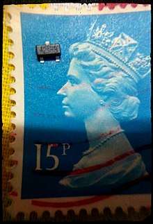
- Discrete semiconductors
- Discrete semiconductors, such as diodes and transistors are often marked with a two- or three-symbol code. The same code marked on different packages or on devices from different manufacturers can translate to different devices. Many of these codes, used because the devices are too small to be marked with more traditional numbers used on larger packages, correlate to more familiar traditional part numbers when a correlation list is consulted. GM4PMK in the United Kingdom has prepared a correlation list, and a similar .pdf list is also available, although these lists are not complete.
- Integrated circuits
- Generally, integrated circuit packages are large enough to be imprinted with the complete part number which includes the manufacturer's specific prefix, or a significant segment of the part number and the manufacturer's name or logo. Examples of manufacturers' specific prefixes include the Philips HEF4066 or Motorola MC14066 (a 4066 Quad Analog Switch) and the Fujitsu Electric FA5502 (a 5502M Boost Architecture power factor correction controller).
See also
- Board-to-board connectors
- Chip carrier
- Electronics
- Electronics manufacturing services
- List of electronics package dimensions
- List of integrated circuit packaging types
- Plastic leaded chip carrier
- Point-to-point construction
- Printed circuit board
- RoHS
- SMT placement equipment
- Through-hole technology
- Wire wrap
- RKM code
References
- Williams, Paul, ed. (1999). Status of the Technology Industry Activities and Action Plan (PDF). Surface Mount Technology. Surface Mount Council. Archived (PDF) from the original on 2015-12-28.
- Schneeweis, Scott. "Artifact: Digital Computer Memory and Circuit Boards, LVDC, Saturn IB/V Guidance, Navigation and Control". Artifacts. Spaceaholic. Archived from the original on 2015-12-28. Retrieved 2015-12-28.
- Jena, Hanings (4 January 2016). "PCB Assembly - Description". www.ourpcb.com. Retrieved 7 February 2018.
- "Why Clean No-Clean?". Assembly Magazine. Retrieved 2017-10-03.
- "No-clean is a process, not a product". www.ipc.org. Retrieved 2017-10-03.
- IPC-A-610E, paragraph 10.6.3.
- Vitoriano, Pedro. "3D Solder Joint Reconstruction on SMD based on 2D Images". Cite journal requires
|journal=(help) - Montrose, Mark I. (1999). "Components and EMC". EMC and the Printed Circuit Board: Design, Theory, and Layout Made Simple. Wiley-Interscience. p. 64. ISBN 978-0780347038.
- "Power Surface Mounts are small, hermetic, surface mountable packages". www.ametek-ecp.com. Retrieved 2017-01-05.
- Judd, Mike; Brindley, Keith (1999). "CS soldering processes". Soldering in Electronics Assembly (2 ed.). Newnes. p. 128. ISBN 978-0750635455.
- Williams, Jim (1991). High Speed Amplifier Techniques - A Designer's Companion for Wideband Circuitry (PDF). Application Notes. Linear Technology. pp. 26–29, 98–121. Archived (PDF) from the original on 2015-12-28. Retrieved 2015-12-28.
- Dr. Lee, Ning-Cheng; Hance, Wanda B. (1993). "Voiding Mechanisms in SMT". Indium Corporation Tech Paper. Retrieved 2015-12-28.
- DerMarderosian, Aaron; Gionet, Vincent (1983). "The Effects of Entrapped Bubbles in Solder Used for the Attachment of Leadless Ceramic Chip Carriers". Reliability Physics Symposium: 235–241. doi:10.1109/IRPS.1983.361989. ISSN 0735-0791.
- "Two Prevalent Rework Heating Methods--Which One is Best?". smt.iconnect007.com. Retrieved 2018-07-27.
- "Resistor SMD code". Resistor Guide. Archived from the original on 2015-12-28. Retrieved 2015-12-28.
| Wikimedia Commons has media related to Surface mount technology. |