List of integrated circuit packaging types
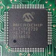
Integrated circuits are put into protective packages to allow easy handling and assembly onto printed circuit boards and to protect the devices from damage. A very large number of different types of package exist. Some package types have standardized dimensions and tolerances, and are registered with trade industry associations such as JEDEC and Pro Electron. Other types are proprietary designations that may be made by only one or two manufacturers. Integrated circuit packaging is the last assembly process before testing and shipping devices to customers.
Occasionally specially-processed integrated circuit dies are prepared for direct connections to a substrate without an intermediate header or carrier. In flip chip systems the IC is connected by solder bumps to a substrate. In beam-lead technology, the metallized pads that would be used for wire bonding connections in a conventional chip are thickened and extended to allow external connections to the circuit. Assemblies using "bare" chips have additional packaging or filling with epoxy to protect the devices from moisture.
Through-hole packages
Through-hole technology uses holes drilled through the PCB for mounting the components. The component has leads that are soldered to pads on the PCB to electrically and mechanically connect them to the PCB.
| Acronym | Full name | Remark |
|---|---|---|
| SIP | Single in-line package | |
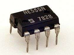
| DIP | Dual in-line package | 0.1 in (2.54 mm) pin spacing, rows 0.3 in (7.62 mm) or 0.6 in (15.24 mm) apart. |
| CDIP | Ceramic DIP[1] | |
| CERDIP | Glass-sealed ceramic DIP[1] | |
| QIP | Quadruple in-line package | Like DIP but with staggered (zig-zag) pins.[1] |
| SKDIP | Skinny DIP | Standard DIP with 0.1 in (2.54 mm) pin spacing, rows 0.3 in (7.62 mm) apart.[1] |
| SDIP | Shrink DIP | Non-standard DIP with smaller 0.07 in (1.78 mm) pin spacing.[1] |
| ZIP | Zig-zag in-line package | |
| MDIP | Molded DIP[2] | |
| PDIP | Plastic DIP[1] |
Surface mount
| Acronym | Full name | Remark |
|---|---|---|
| CCGA | Ceramic column-grid array (CGA)[3] | |
| CGA | Column-grid array[3] | Example |
| CERPACK | Ceramic package[4] | |
| CQGP[5] | ||
| LLP | Lead-less lead-frame package | A package with metric pin distribution (0.5–0.8 mm pitch)[6] |
| LGA | Land grid array[3] | |
| LTCC | Low-temperature co-fired ceramic[7] | |
| MCM | Multi-chip module[8] | |
| MICRO SMDXT | Micro surface-mount device extended technology[9] | Example |
Chip on board is a packaging technique that directly connects a die to a PCB, without an interposer or lead frame.
Chip carrier
A chip carrier is a rectangular package with contacts on all four edges. Leaded chip carriers have metal leads wrapped around the edge of the package, in the shape of a letter J. Leadless chip carriers have metal pads on the edges. Chip carrier packages may be made of ceramic or plastic and are usually secured to a printed circuit board by soldering, though sockets can be used for testing.
| Acronym | Full name | Remark |
|---|---|---|
| BCC | Bump chip carrier[3] | - |
| CLCC | Ceramic lead-less chip carrier[1] | - |
| LCC | Lead-less chip carrier[3] | Contacts are recessed vertically. |
| LCC | Leaded chip carrier[3] | - |
| LCCC | Leaded ceramic-chip carrier[3] | - |
| DLCC | Dual lead-less chip carrier (ceramic)[3] | - |
| PLCC | Plastic leaded chip carrier[1][3] | - |
Pin grid arrays
| Acronym | Full name | Remark |
|---|---|---|
| OPGA | Organic pin-grid array | - |
| FCPGA | Flip-chip pin-grid array[3] | - |
| PAC | Pin array cartridge[10] | - |
| PGA | Pin-grid array | Also known as PPGA[1] |
| CPGA | Ceramic pin-grid array[3] | - |
Flat packages
| Acronym | Full name | Remark |
|---|---|---|
| - | Flat-pack | Earliest version metal/ceramic packaging with flat leads |
| CFP | Ceramic flat-pack[3] | - |
| CQFP | Ceramic quad flat-pack[1][3] | Similar to PQFP |
| BQFP | Bumpered quad flat-pack[3] | - |
| DFN | Dual flat-pack | No lead[3] |
| ETQFP | Exposed thin quad flat-package[11] | - |
| PQFN | Power quad flat-pack | No-leads, with exposed die-pad[s] for heatsinking[12] |
| PQFP | Plastic quad flat-package[1][3] | - |
| LQFP | Low-profile quad flat-package[3] | - |
| QFN | Quad flat no-leads package | Also called as micro lead frame (MLF).[3][13] |
| QFP | Quad flat package[1][3] | - |
| MQFP | Metric quad flat-pack | QFP with metric pin distribution[3] |
| HVQFN | Heat-sink very-thin quad flat-pack, no-leads | - |
| SIDEBRAZE[14][15] | ||
| TQFP | Thin quad flat-pack[1][3] | - |
| VQFP | Very-thin quad flat-pack[3] | - |
| TQFN | Thin quad flat, no-lead | - |
| VQFN | Very-thin quad flat, no-lead | - |
| WQFN | Very-very-thin quad flat, no-lead | - |
| UQFN | Ultra-thin quad flat-pack, no-lead | - |
| ODFN | Optical dual flat, no-lead | IC packaged in transparent packaging used in optical sensor |
Small outline packages
| Acronym | Full name | Remark |
|---|---|---|
| SOP | Small-outline package[1] | |
| CSOP | Ceramic small-outline package | |
| DSOP | Dual small-outline package | |
| HSOP | Thermally-enhanced small-outline package | |
| mini-SOIC | Mini small-outline integrated circuit | |
| MSOP | Mini small-outline package | |
| PSOP | Plastic small-outline package[3] | |
| PSON | Plastic small-outline no-lead package | |
| QSOP | Quarter-size small-outline package | The pin spacing are width of 0.635 mm.[3] |
| SOIC | Small-outline integrated circuit | Also known as SOIC NARROW and SOIC WIDE |
| SOJ | Small-outline J-leaded package | |
| SON | Small-outline no-lead package | |
| SSOP | Shrink small-outline package[3] | |
| TSOP | Thin small-outline package[3] | Example |
| TSSOP | Thin shrink small-outline package[3] | |
| TVSOP | Thin very-small-outline package[3] | |
| µMAX | Similar to a SOIC. (A Maxim trademark example) | |
| WSON | Very-very-thin small-outline no-lead package | |
| USON | Very-very-thin small-outline no-lead package | Slightly smaller than WSON |
Chip-scale packages
| Acronym | Full name | Remark |
|---|---|---|
| BL | Beam lead technology | Bare silicon chip, an early chip-scale package |
| CSP | Chip-scale package | Package size is no more than 1.2× the size of the silicon chip[16][17] |
| TCSP | True chip-size package | Package is same size as silicon[18] |
| TDSP | True die-size package | Same as TCSP[18] |
| WCSP or WL-CSP or WLCSP | Wafer-level chip-scale package | A WL-CSP or WLCSP package is just a bare Die with a redistribution layer (or I/O pitch) to rearrange the pins or contacts on the die so that they can be big enough and have sufficient spacing so that they can be handled just like a BGA package.[19] |
| PMCP | Power Mount CSP (Chip Scale Package) | Variation of WLCSP, for power devices like MOSFETs. Made by Panasonic. [20] |
| Fan-out WLCSP | Fan-out wafer-level packaging | Variation of WLCSP. Like a BGA package but with the interposer built directly atop the die and encapsulated along the rest of the chip. |
| eWLB | Embedded Wafer Level Ball Grid Array | Variation of WLCSP. |
| MICRO SMD | - | Chip-size package (CSP) developed by National Semiconductor[21] |
| COB | Chip-on-board | Bare silicon chip, that is usually an integrated circuit, is supplied without a package. It can often be identified by having a blob of black Epoxy instead of a square package. Also used for LEDs. In LEDs, transparent epoxy or a silicon caulk-like material that may containin a phosphor is poured into a mold containing the LED and cured. The mold forms part of the package. |
| COF | Chip-on-flex | Variation of COB, where a chip is mounted directly to a flex circuit. |
| TAB | Tape-automated bonding | Variation of COF, where a flip chip is mounted directly to a flex circuit without the use of bonding wires. |
| COG | Chip-on-glass | Variation of COB, where a chip is mounted directly to a piece of glass - typically an LCD. Used by LCD and OLED driver ICs. |
Ball grid array
Ball Grid Array BGA uses the underside of the package to place pads with balls of solder in grid pattern as connections to PCB.[1][3]
| Acronym | Full name | Remark |
|---|---|---|
| FBGA | Fine-pitch ball-grid array | A square or rectangular array of solder balls on one surface[3] |
| LBGA | Low-profile ball-grid array | Also known as laminate ball-grid array[3] |
| TEPBGA | Thermally-enhanced plastic ball-grid array | - |
| CBGA | Ceramic ball-grid array[3] | - |
| OBGA | Organic ball-grid array[3] | - |
| TFBGA | Thin fine-pitch ball-grid array[3] | - |
| PBGA | Plastic ball-grid array[3] | - |
| MAP-BGA | Mold array process - ball-grid array | - |
| UCSP | Micro (μ) chip-scale package | Similar to a BGA (A Maxim trademark example)[17] |
| μBGA | Micro ball-grid array | Ball spacing less than 1 mm |
| LFBGA | Low-profile fine-pitch ball-grid array[3] | - |
| TBGA | Thin ball-grid array[3] | - |
| SBGA | Super ball-grid array[3] | Above 500 balls |
| UFBGA | Ultra-fine ball-grid array[3] |
Transistor, diode, small-pin-count IC packages
.svg.png)
- MELF: Metal electrode leadless face (usually for resistors and diodes)
- SOD: Small-outline diode.
- SOT: Small-outline transistor (also SOT-23, SOT-223, SOT-323).
- TO-XX: wide range of small pin count packages often used for discrete parts like transistors or diodes.
- TO-3: Panel-mount with leads
- TO-5: Metal can package with radial leads
- TO-18: Metal can package with radial leads
- TO-39
- TO-46
- TO-66: Similar shape to the TO-3 but smaller
- TO-92: Plastic-encapsulated package with three leads
- TO-99: Metal can package with eight radial leads
- TO-100
- TO-126: Plastic-encapsulated package with three leads and a hole for mounting on a heat sink
- TO-220: Through-hole plastic package with a (usually) metal heat sink tab and three leads
- TO-226[22]
- TO-247:[23] Plastic-encapsulated package with three leads and a hole for mounting on a heat sink
- TO-251:[23] Also called IPAK: SMT package similar to the DPAK but with longer leads for SMT or TH mounting
- TO-252:[23] (also called SOT428, DPAK):[23] SMT package similar to the DPAK but smaller
- TO-262:[23] Also called I2PAK: SMT package similar to the D2PAK but with longer leads for SMT or TH mounting
- TO-263:[23] Also called D2PAK: SMT package similar to the TO-220 without the extended tab and mounting hole
- TO-274:[23] Also called Super-247: SMT package similar to the TO-247 without the mounting hole
Dimension reference
Surface-mount
- C
- Clearance between IC body and PCB
- H
- Total Height
- T
- Lead Thickness
- L
- Total carrier length
- LW
- Lead width
- LL
- Lead length
- P
- Pitch
Through-hole
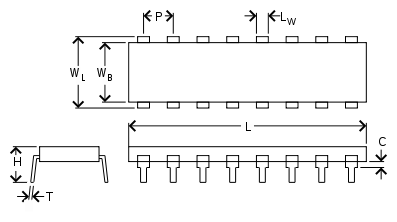
- C
- Clearance between IC body and board
- H
- Total height
- T
- Lead thickness
- L
- Total carrier length
- LW
- Lead width
- LL
- Lead length
- P
- Pitch
- WB
- IC body width
- WL
- Lead-to-lead width
Package dimensions
All measurements below are given in mm. To convert mm to mils, divide mm by 0.0254 (i.e., 2.54 mm / 0.0254 = 100 mil).
- C
- Clearance between package body and PCB.
- H
- Height of package from pin tip to top of package.
- T
- Thickness of pin.
- L
- Length of package body only.
- LW
- Pin width.
- LL
- Pin length from package to pin tip.
- P
- Pin pitch (distance between conductors to the PCB).
- WB
- Width of the package body only.
- WL
- Length from pin tip to pin tip on the opposite side.
Dual row
| Image | Family | Pin | Name | Package | WB | WL | H | C | L | P | LL | T | LW |
|---|---|---|---|---|---|---|---|---|---|---|---|---|---|
|
DIP | Y | Dual inline package | 8-DIP | 6.2–6.48 | 7.62 | 7.7 | 9.2–9.8 | 2.54 (0.1 in) | 3.05–3.6 | 1.14–1.73 | ||
| 32-DIP | 15.24 | 2.54 (0.1 in) | |||||||||||
| LFCSP | N | Lead-frame chip-scale package | 0.5 | ||||||||||
 |
MSOP | Y | Mini small-outline package | 8-MSOP | 3 | 4.9 | 1.1 | 0.10 | 3 | 0.65 | 0.95 | 0.18 | 0.17–0.27 |
| 10-MSOP | 3 | 4.9 | 1.1 | 0.10 | 3 | 0.5 | 0.95 | 0.18 | 0.17–0.27 | ||||
| 16-MSOP | 3 | 4.9 | 1.1 | 0.10 | 4.04 | 0.5 | 0.95 | 0.18 | 0.17–0.27 | ||||
 |
SO SOIC SOP |
Y | Small-outline integrated circuit | 8-SOIC | 3.9 | 5.8–6.2 | 1.72 | 0.10–0.25 | 4.8–5.0 | 1.27 | 1.05 | 0.19–0.25 | 0.39–0.46 |
| 14-SOIC | 3.9 | 5.8–6.2 | 1.72 | 0.10–0.25 | 8.55–8.75 | 1.27 | 1.05 | 0.19–0.25 | 0.39–0.46 | ||||
| 16-SOIC | 3.9 | 5.8–6.2 | 1.72 | 0.10–0.25 | 9.9–10 | 1.27 | 1.05 | 0.19–0.25 | 0.39–0.46 | ||||
| 16-SOIC | 7.5 | 10.00–10.65 | 2.65 | 0.10–0.30 | 10.1–10.5 | 1.27 | 1.4 | 0.23–0.32 | 0.38–0.40 | ||||
 | SOT | Y | Small-outline transistor | SOT-23-6 | 1.6 | 2.8 | 1.45 | 2.9 | 0.95 | 0.6 | 0.22–0.38 | ||
| SSOP | Y | Shrink small-outline package | 0.65 | ||||||||||
| TDFN | N | Thin dual flat no-lead | 8-TDFN | 3 | 3 | 0.7–0.8 | 3 | 0.65 | N/A | 0.19–0.3 | |||
| TSOP | Y | Thin small-outline package | 0.5 | ||||||||||
| TSSOP | Y | Thin shrink small-outline package | 8-TSSOP | 4.4 | 6.4 | 1.2 | 0.15 | 3 | 0.65 | 0.09–0.2 | 0.19–0.3 | ||
| µSOP | Y | Micro small-outline package[24] | µSOP-8 | 4.9 | 1.1 | 3 | 0.65 | ||||||
| US8[25] | Y | US8 package | 2.3 | 3.1 | .7 | 2 | 0.5 |
Quad rows
| Image | Family | Pin | Name | Package | WB | WL | H | C | L | P | LL | T | LW |
|---|---|---|---|---|---|---|---|---|---|---|---|---|---|
 | PLCC | N | Plastic leaded chip-carrier | 1.27 | |||||||||
| CLCC | N | Ceramic leadless chip-carrier | 48-CLCC | 14.22 | 14.22 | 2.21 | 14.22 | 1.016 | N/A | 0.508 | |||
| LQFP | Y | Low-profile Quad Flat Package | 0.50 | ||||||||||
 | TQFP | Y | Thin quad flat-package | TQFP-44 | 10.00 | 12.00 | 0.35–0.50 | 0.80 | 1.00 | 0.09–0.20 | 0.30–0.45 | ||
| TQFN | N | Thin quad flat no-lead |
LGA
| Package | x | y | z |
|---|---|---|---|
| 52-ULGA | 12 mm | 17 mm | 0.65 mm |
| 52-ULGA | 14 mm | 18 mm | 0.10 mm |
| 52-VELGA | ? | ? | ? |
Multi-chip packages
A variety of techniques for interconnecting several chips within a single package have been proposed and researched:
- SiP (system in package)
- PoP (package on package)
- 3D-SICs, Monolithic 3D ICs, and other three-dimensional integrated circuits
- Multi-chip module
- WSI (wafer-scale integration)
- proximity communication[26]
By terminal count
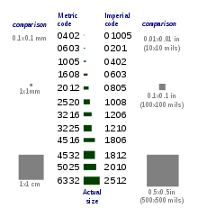
Surface-mount components are usually smaller than their counterparts with leads, and are designed to be handled by machines rather than by humans. The electronics industry has standardized package shapes and sizes (the leading standardisation body is JEDEC).
The codes given in the chart below usually tell the length and width of the components in tenths of millimeters or hundredths of inches. For example, a metric 2520 component is 2.5 mm by 2.0 mm which corresponds roughly to 0.10 inches by 0.08 inches (hence, imperial size is 1008). Exceptions occur for imperial in the two smallest rectangular passive sizes. The metric codes still represent the dimensions in mm, even though the imperial size codes are no longer aligned. Problematically, some manufacturers are developing metric 0201 components with dimensions of 0.25 mm × 0.125 mm (0.0098 in × 0.0049 in),[27] but the imperial 01005 name is already being used for the 0.4 mm × 0.2 mm (0.0157 in × 0.0079 in) package. These increasingly small sizes, especially 0201 and 01005, can sometimes be a challenge from a manufacturability or reliability perspective.[28]
Two-terminal packages
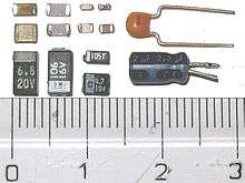
Rectangular passive components
Mostly resistors and capacitors.
| Package | Approximate dimensions, length × width | Typical resistor power rating (W) | ||
|---|---|---|---|---|
| Metric | Imperial | |||
| 0201 | 008004 | 0.25 mm × 0.125 mm | 0.010 in × 0.005 in | |
| 03015 | 009005 | 0.3 mm × 0.15 mm | 0.012 in × 0.006 in | 0.02[29] |
| 0402 | 01005 | 0.4 mm × 0.2 mm | 0.016 in × 0.008 in | 0.031[30] |
| 0603 | 0201 | 0.6 mm × 0.3 mm | 0.02 in × 0.01 in | 0.05[30] |
| 1005 | 0402 | 1.0 mm × 0.5 mm | 0.04 in × 0.02 in | 0.062[31]–0.1[30] |
| 1608 | 0603 | 1.6 mm × 0.8 mm | 0.06 in × 0.03 in | 0.1[30] |
| 2012 | 0805 | 2.0 mm × 1.25 mm | 0.08 in × 0.05 in | 0.125[30] |
| 2520 | 1008 | 2.5 mm × 2.0 mm | 0.10 in × 0.08 in | |
| 3216 | 1206 | 3.2 mm × 1.6 mm | 0.125 in × 0.06 in | 0.25[30] |
| 3225 | 1210 | 3.2 mm × 2.5 mm | 0.125 in × 0.10 in | 0.5[30] |
| 4516 | 1806 | 4.5 mm × 1.6 mm | 0.18 in × 0.06 in[32] | |
| 4532 | 1812 | 4.5 mm × 3.2 mm | 0.18 in × 0.125 in | 0.75[30] |
| 4564 | 1825 | 4.5 mm × 6.4 mm | 0.18 in × 0.25 in | 0.75[30] |
| 5025 | 2010 | 5.0 mm × 2.5 mm | 0.20 in × 0.10 in | 0.75[30] |
| 6332 | 2512 | 6.3 mm × 3.2 mm | 0.25 in × 0.125 in | 1[30] |
| 6863 | 2725 | 6.9 mm × 6.3 mm | 0.27 in × 0.25 in | 3 |
| 7451 | 2920 | 7.4 mm × 5.1 mm | 0.29 in × 0.20 in[33] | |
Tantalum capacitors[34][35]
| Package | Dimensions (Length, typ. × width, typ. × height, max.) |
|---|---|
| EIA 2012-12 (KEMET R, AVX R) | 2.0 mm × 1.3 mm × 1.2 mm |
| EIA 3216-10 (KEMET I, AVX K) | 3.2 mm × 1.6 mm × 1.0 mm |
| EIA 3216-12 (KEMET S, AVX S) | 3.2 mm × 1.6 mm × 1.2 mm |
| EIA 3216-18 (KEMET A, AVX A) | 3.2 mm × 1.6 mm × 1.8 mm |
| EIA 3528-12 (KEMET T, AVX T) | 3.5 mm × 2.8 mm × 1.2 mm |
| EIA 3528-21 (KEMET B, AVX B) | 3.5 mm × 2.8 mm × 2.1 mm |
| EIA 6032-15 (KEMET U, AVX W) | 6.0 mm × 3.2 mm × 1.5 mm |
| EIA 6032-28 (KEMET C, AVX C) | 6.0 mm × 3.2 mm × 2.8 mm |
| EIA 7260-38 (KEMET E, AVX V) | 7.2 mm × 6.0 mm × 3.8 mm |
| EIA 7343-20 (KEMET V, AVX Y) | 7.3 mm × 4.3 mm × 2.0 mm |
| EIA 7343-31 (KEMET D, AVX D) | 7.3 mm × 4.3 mm × 3.1 mm |
| EIA 7343-43 (KEMET X, AVX E) | 7.3 mm × 4.3 mm × 4.3 mm |
Aluminum capacitors[36][37][38]
| Package | Dimensions (Length, typ. × width, typ. × height, max.) |
|---|---|
| CDE A | 3.3 mm × 3.3 mm x 5.5 mm |
| Panasonic B, Chemi-Con D | 4.3 mm × 4.3 mm x 6.1 mm (5.7 mm for Chemi-Con) |
| Panasonic C, Chemi-Con E | 5.3 mm × 5.3 mm x 6.1 mm (5.7 mm for Chemi-Con) |
| Panasonic D, Chemi-Con F | 6.6 mm × 6.6 mm x 6.1 mm (5.7 mm for Chemi-Con) |
| Panasonic E/F, Chemi-Con H | 8.3 mm × 8.3 mm x 6.5 mm |
| Panasonic G, Chemi-Con J | 10.3 mm × 10.3 mm x 10.5 mm |
| Chemi-Con K | 13 mm × 13 mm x 14 mm |
| Panasonic H | 13.5 mm × 13.5 mm x 14 mm |
| Panasonic J, Chemi-Con L | 17 mm × 17 mm x 17 mm |
| Panasonic K, Chemi-Con M | 19 mm × 19 mm x 17 mm |
Small-outline diode (SOD)
| Package | Dimensions (Length, typ. × width, typ. × height, max.) |
|---|---|
| SOD-80C | 3.5 mm × ⌀ 1.5 mm[39] |
| SOD-123 | 2.65 mm × 1.6 mm × 1.35 mm[40] |
| SOD-128 | 3.8 mm × 2.5 mm × 1.1 mm[41] |
| SOD-323 (SC-90) | 1.7 mm × 1.25 mm × 1.1 mm[42] |
| SOD-523 (SC-79) | 1.2 mm × 0.8 mm × 0.65 mm[43] |
| SOD-723 | 1.4 mm × 0.6 mm × 0.65 mm[44] |
| SOD-923 | 0.8 mm × 0.6 mm × 0.4 mm[45] |
Metal electrode leadless face[46] (MELF)
Mostly resistors and diodes; barrel shaped components, dimensions do not match those of rectangular references for identical codes.
| Package | Dimensions |
Typical resistor rating | |
|---|---|---|---|
| Power (W) | Voltage (V) | ||
| MicroMelf (MMU), 0102 | 2.2 mm × ⌀ 1.1 mm | 0.2–0.3 | 150 |
| MiniMelf (MMA), 0204 | 3.6 mm × ⌀ 1.4 mm | 0.25–0.4 | 200 |
| Melf (MMB), 0207 | 5.8 mm × ⌀ 2.2 mm | 0.4–1.0 | 300 |
DO-214
Commonly used for rectifier, Schottky, and other diodes.
| Package | Dimensions (incl. leads) (Length, typ. × width, typ. × height, max.) |
|---|---|
| DO-214AA (SMB) | 5.4 mm × 3.6 mm × 2.65 mm[47] |
| DO-214AB (SMC) | 7.95 mm × 5.9 mm × 2.25 mm[47] |
| DO-214AC (SMA) | 5.2 mm × 2.6 mm × 2.15 mm[47] |
Three- and four-terminal packages
Small-outline transistor (SOT)
| Package | Dimensions (Length, typ. × width, typ. × height, max.) |
|---|---|
| SOT-23-3 (TO-236-3) (SC-59) | 2.92 mm × 1.3 mm × 1.12 mm body: three terminals.[48] |
| SOT-89 (TO-243)[49] (SC-62)[50] | 4.5 mm × 2.5 mm × 1.5 mm body: four terminals, center pin is connected to a large heat-transfer pad.[51] |
| SOT-143 (TO-253) | 2.9 mm × 1.3 mm × 1.22 mm tapered body: four terminals: one larger pad denotes terminal 1.[52] |
| SOT-223 (TO-261) | 6.5 mm × 3.5 mm × 1.8 mm body: four terminals, one of which is a large heat-transfer pad.[53] |
| SOT-323 (SC-70) | 2 mm × 1.25 mm × 1.1 mm body: three terminals.[54] |
| SOT-416 (SC-75) | 1.6 mm × 0.8 mm × 0.9 mm body: three terminals.[55] |
| SOT-663 | 1.6 mm × 1.2 mm × 0.6 mm body: three terminals.[56] |
| SOT-723 | 1.2 mm × 0.8 mm × 0.55 mm body: three terminals: flat lead.[57] |
| SOT-883 (SC-101) | 1 mm × 0.6 mm × 0.5 mm body: three terminals: leadless.[58] |
Other
- DPAK (TO-252, SOT-428): Discrete Packaging. Developed by Motorola to house higher powered devices. Comes in three[59] or five-terminal[60] versions.
- D2PAK (TO-263, SOT-404): Bigger than the DPAK; basically a surface mount equivalent of the TO220 through-hole package. Comes in 3, 5, 6, 7, 8 or 9-terminal versions.[61]
- D3PAK (TO-268): Even larger than D2PAK.[62]
Five- and six-terminal packages
Small-outline transistor (SOT)
| Package | Dimensions (Length, typ. × width, typ. × height, max.) |
|---|---|
| SOT-23-6 (SOT-26) (SC-74) | 2.9 mm × 1.3 mm × 1.3 mm body: six terminals.[63] |
| SOT-353 (SC-88A) | 2 mm × 1.25 mm × 0.95 mm body: five terminals.[64] |
| SOT-363 (SC-88, SC-70-6) | 2 mm × 1.25 mm × 0.95 mm body: six terminals.[65] |
| SOT-563 | 1.6 mm × 1.2 mm × 0.6 mm body: six terminals.[66] |
| SOT-665 | 1.6 mm × 1.6 mm × 0.55 mm body: five terminals.[67] |
| SOT-666 | 1.6 mm × 1.2 mm × 0.6 mm body: six terminals.[68] |
| SOT-886 | 1.45 mm × 1 mm × 0.5 mm body: six terminals: leadless.[69] |
| SOT-891 | 1 mm × 1 mm × 0.5 mm body: five terminals: leadless.[70] |
| SOT-953 | 1 mm × 0.8 mm × 0.5 mm body: five terminals.[71] |
| SOT-963 | 1 mm × 1 mm × 0.5 mm body: six terminals.[72] |
| SOT-1115 | 1 mm × 0.9 mm × 0.35 mm body: six terminals: leadless.[73] |
| SOT-1202 | 1 mm × 1 mm × 0.35 mm body: six terminals: leadless.[74] |

Packages with more than six terminals
Dual-in-line
- Flatpack was one of the earliest surface-mounted packages.
- Small-outline integrated circuit (SOIC): dual-in-line, 8 or more pins, gull-wing lead form, pin spacing 1.27 mm.
- Small-outline package, J-leaded (SOJ): The same as SOIC except J-leaded.[75]
- Thin small-outline package (TSOP): thinner than SOIC with smaller pin spacing of 0.5 mm.
- Shrink small-outline package (SSOP): pin spacing of 0.65 mm, sometimes 0.635 mm or in some cases 0.8 mm.
- Thin shrink small-outline package (TSSOP).
- Quarter-size small-outline package (QSOP): with pin spacing of 0.635 mm.
- Very small outline package (VSOP): even smaller than QSOP; 0.4-, 0.5-, or 0.65-mm pin spacing.
- Dual flat no-lead (DFN): smaller footprint than leaded equivalent.
Quad-in-line
- Plastic leaded chip carrier (PLCC): square, J-lead, pin spacing 1.27 mm
- Quad flat package (QFP): various sizes, with pins on all four sides
- Low-profile quad flat-package (LQFP): 1.4 mm high, varying sized and pins on all four sides
- Plastic quad flat-pack (PQFP), a square with pins on all four sides, 44 or more pins
- Ceramic quad flat-pack (CQFP): similar to PQFP
- Metric quad flat-pack (MQFP): a QFP package with metric pin distribution
- Thin quad flat-pack (TQFP), a thinner version of LQFP
- Quad flat no-lead (QFN): smaller footprint than leaded equivalent
- Leadless chip carrier (LCC): contacts are recessed vertically to "wick-in" solder. Common in aviation electronics because of robustness to mechanical vibration.
- Micro leadframe package (MLP, MLF): with a 0.5 mm contact pitch, no leads (same as QFN)
- Power quad flat no-lead (PQFN): with exposed die-pads for heatsinking
Grid arrays
- Ball grid array (BGA): A square or rectangular array of solder balls on one surface, ball spacing typically 1.27 mm (0.050 in)
- Land grid array (LGA): An array of bare lands only. Similar to in appearance to QFN, but mating is by spring pins within a socket rather than solder.
- Fine-pitch ball grid array (FBGA): A square or rectangular array of solder balls on one surface
- Low-profile fine-pitch ball grid array (LFBGA): A square or rectangular array of solder balls on one surface, ball spacing typically 0.8 mm
- Thin fine-pitch ball grid array (TFBGA): A square or rectangular array of solder balls on one surface, ball spacing typically 0.5 mm
- Column grid array (CGA): A circuit package in which the input and output points are high-temperature solder cylinders or columns arranged in a grid pattern.
- Ceramic column grid array (CCGA): A circuit package in which the input and output points are high-temperature solder cylinders or columns arranged in a grid pattern. The body of the component is ceramic.
- Micro ball grid array (μBGA): Ball spacing less than 1 mm
- Lead-less package (LLP): A package with metric pin distribution (0.5 mm pitch).
Non-packaged devices
Although surface-mount, these devices require specific process for assembly.
- Chip-on-board (COB), a bare silicon chip, that is usually an integrated circuit, is supplied without a package (which is usually a lead frame overmolded with epoxy) and is attached, often with epoxy, directly to a circuit board. The chip is then wire bonded and protected from mechanical damage and contamination by an epoxy "glob-top".
- Chip-on-flex (COF), a variation of COB, where a chip is mounted directly to a flex circuit. Tape-automated bonding process is also a chip-on-flex process as well.
- Chip-on-glass (COG), a variation of COB, where a chip, typically a liquid crystal display (LCD) controller, is mounted directly on glass.
- Chip-on-wire (COW), a variation of COB, where a chip, typically a LED or RFID chip, is mounted directly on wire, thus making it a very thin and flexible wire. Such wire may then be covered with cotton, glass or other materials to make into smart textiles or electronic textiles.
There are often subtle variations in package details from manufacturer to manufacturer, and even though standard designations are used, designers need to confirm dimensions when laying out printed circuit boards.
See also
- Surface-mount technology
- Three-dimensional integrated circuit
- Interposer
- IPC (electronics)
- List of chip carriers
- List of electronics package dimensions
- Redistribution layer
- Surface-mounted package sizes
- Wafer-level packaging
References
- "CPU Collection Museum - Chip Package Information". The CPU Shack. Retrieved 2011-12-15.
- "Archived copy" (PDF). Archived from the original (PDF) on 2011-08-15. Retrieved 2011-02-03.CS1 maint: archived copy as title (link)
- "Integrated Circuit, IC Package Types; SOIC. Surface Mount Device Package". Interfacebus.com. Retrieved 2011-12-15.
- "National Semiconductor CERPACK Package Products". National.com. Archived from the original on 2012-02-18. Retrieved 2011-12-15.
- "National Semiconductor CQGP Package Products". National.com. Archived from the original on 2007-10-21. Retrieved 2011-12-15.
- "National's LLP Package". National.com. Archived from the original on 2011-02-13. Retrieved 2011-12-15.
- "LTCC Low Temperature Co-fired Ceramic". Minicaps.com. Retrieved 2011-12-15.
- Frye, R.C.; Gabara, T.J.; Tai, K.L.; Fischer, W.C.; Knauer, S.C. (1993). "Performance evaluation of MCM chip-to-chip interconnections using custom I/O buffer designs". Sixth Annual IEEE International ASIC Conference and Exhibit. Ieeexplore.ieee.org. pp. 464–467. doi:10.1109/ASIC.1993.410760. ISBN 978-0-7803-1375-0.
- "National Semiconductor Launches New Generation of Ultra-Miniature, High Pin-Count Integrated Circuit Packages". National.com. Archived from the original on 2012-02-18. Retrieved 2011-12-15.
- Meyers, Michael; Jernigan, Scott (2004). Mike Meyers' A+ Guide to PC Hardware. The McGraw-Hill Companies. ISBN 978-0-07-223119-9.
- Archived August 18, 2011, at the Wayback Machine
- "Press Releases - Motorola Mobility, Inc". Motorola.com. Retrieved 2011-12-15.
- "Xilinx new CPLDs with two I/O banks". Eetasia.com. 2004-12-08. Retrieved 2011-12-15.
- "Packages". Chelseatech.com. 2010-11-15. Retrieved 2011-12-15.
- "Archived copy". Archived from the original on 2008-11-20. Retrieved 2009-10-24.CS1 maint: archived copy as title (link)
- "CSP - Chip Scale Package". Siliconfareast.com. Retrieved 2011-12-15.
- "Understanding Flip-Chip and Chip-Scale Package Technologies and Their Applications - Maxim". Maxim-ic.com. 2007-04-18. Retrieved 2011-12-15.
- "Chip Scale Review Online". Chipscalereview.com. Retrieved 2011-12-15.
- https://www.nxp.com/docs/en/application-note/AN3846.pdf
- https://na.industrial.panasonic.com/products/semiconductors/mosfets
- "Packaging Technology | National Semiconductor – Package Drawings, Part Marking, Package Codes, LLP, micro SMD, Micro-Array". National.com. Archived from the original on 2010-08-01. Retrieved 2011-12-15.
- http://www.siliconfareast.com/to226.htm
- http://www.irf.com/package/
- http://pdfserv.maximintegrated.com/package_dwgs/21-0036.PDF
- "Fairchild's TinyLogic family overview" (PDF). March 22, 2013. Archived from the original (PDF) on January 8, 2015.
- Proximity Communication - the Technology, 2004, archived from the original on 2009-07-18
- Murata, Tsuneo (2012-09-05). "Murata's world's Smallest Monolithic Ceramic Capacitor - 0201 <millimeter size> size (0.25 mm x 0.125 mm)" (Press release). Kyoto, Japan: Murata Manufacturing Co., Ltd. Archived from the original on 2015-12-28. Retrieved 2015-12-28.
- "White Paper 0201 and 01005 Adoption in Industry" (PDF). Retrieved 7 February 2018.
- "SMR Series Ultra-Compact Chip Resistors" (PDF). Datasheet. Rohm Semiconductor.
- "Thick Film Chip Resistors" (PDF). Datasheet. Panasonic. Archived from the original (PDF) on 2014-02-09.
- "Thick Film Chip Resistor - SMDC Series" (PDF). Datasheet. electronic sensor + resistor GmbH. Archived from the original (PDF) on 2015-12-28. Retrieved 2015-12-28.
- "SMD/BLOCK Type EMI Suppression Filters EMIFIL" (PDF). Catalog. Murata Manufacturing Co., Ltd. Archived from the original on 2015-12-28. Retrieved 2015-12-28.
- "POLYFUSE® Resettable Fuses SMD2920" (PDF). Datasheet. Littelfuse. Retrieved 2015-12-28.
- "TLJ Series - Tantalum Solid Electrolytic Chip Capacitors High CV Consumer Series" (PDF). Datasheet. AVX Corporation. Archived (PDF) from the original on 2015-12-28. Retrieved 2015-12-28.
- "Tantalum Surface Mount Capacitors - Standard Tantalum" (PDF). Catalog. KEMET Electronics Corporation. 2011-09-06. Archived from the original (PDF) on 2011-12-26. Retrieved 2015-12-28.
- "SMT Aluminum Electrolytic Capacitors" (PDF). Datasheet. Panasonic. Archived from the original (PDF) on 2012-03-01. Retrieved 2015-12-28.
- "Application Guide - Aluminum SMT Capacitors" (PDF). Resources. Cornell Dubilier. Archived (PDF) from the original on 2015-12-28. Retrieved 2015-12-28.
- "Surface Mount Aluminum Electrolytic Capacitors - Alchip-MVA Series" (PDF). Nippon Chemi-Con. Retrieved 2015-12-28.
- "SOD 80C Hermetically sealed glass surface-mounted package" (PDF). NXP Semiconductors. Archived (PDF) from the original on 2012-04-23. Retrieved 2015-12-28.
- "Designer's™ Data Sheet - Surface Mount Silicon Zener Diodes - Plastic SOD-123 Package" (PDF). Motorola. Retrieved 2015-12-28.
- "SOD128 plastic, surface mounted package" (PDF). NXP Semiconductors. 2017. Archived (PDF) from the original on 2015-12-28. Retrieved 2015-12-28.
- "SOD323 plastic, surface-mounted package" (PDF). NXP Semiconductors. 2019. Archived (PDF) from the original on 2012-11-19. Retrieved 2015-12-28.
- "SOD523 Package outline" (PDF). NXP Semiconductors. 2008. Archived (PDF) from the original on 2015-12-28. Retrieved 2015-12-28.
- "Comchip CDSP400-G" (PDF). Datasheet. Comchip Technology Corporation. Archived (PDF) from the original on 2015-12-28. Retrieved 2015-12-28.
- "SOD923 Microlead ultra small surface-mounted plastic package" (PDF). Datasheet. NXP Semiconductors.
- "Professional Thin Film MELF Resistors" (PDF). Vishay Intertechnology. 2014-04-22. Archived (PDF) from the original on 2015-12-28. Retrieved 2015-12-28.
- "Package Outline Dimensions - U-DFN1616-6 (Type F)" (PDF). Diodes Incorporated. Archived (PDF) from the original on 2015-12-28. Retrieved 2015-12-28.
- "Package Outline Drawing - P3.064" (PDF). Intersil. Archived (PDF) from the original on 2015-12-28. Retrieved 2015-12-28.
- "3-Lead Small Outline Transistor Package [SOT-89] (RK-3)" (PDF). Analog Devices. 2013-09-12. Archived (PDF) from the original on 2015-12-28. Retrieved 2015-12-28.
- "Standards for the Dimensions of Semiconductor Devices" (PDF). Electronic Industries Association of Japan. 1996-04-15. Archived (PDF) from the original on 2015-12-28. Retrieved 2015-12-28.
- "Package Information - SOT-89" (PDF). RICOH. Archived (PDF) from the original on 2015-12-28. Retrieved 2015-12-28.
- https://www.analog.com/media/en/package-pcb-resources/package/pkg_pdf/sot-143ra/ra_4.pdf
- "SOT-233 Molded Package" (PDF). Fairchild Semiconductor. 2008-02-26. Archived (PDF) from the original on 2015-12-28. Retrieved 2015-12-28.
- "SOT323 Package outline" (PDF). NXP Semiconductors. 2008. Archived from the original (PDF) on 2015-12-28. Retrieved 2015-12-28.
- "SOT416 Package outline" (PDF). NXP Semiconductors. 2010. Archived from the original (PDF) on 2015-12-28. Retrieved 2015-12-28.
- "SOT663 Package outline" (PDF). NXP Semiconductors. 2008. Archived (PDF) from the original on 2015-12-28. Retrieved 2015-12-28.
- "Mechanical Case Outline SOT-723" (PDF). ON Semiconductor. 2009-08-10. Retrieved 2015-12-28.
- "SOT883 Package outline" (PDF). NXP Semiconductors. 2008. Archived (PDF) from the original on 2015-12-28. Retrieved 2015-12-28.
- "D-PAK (TO-252AA) Outline Dimensions" (PDF). Vishay Intertechnology. 2012-12-05. Archived (PDF) from the original on 2015-12-28. Retrieved 2015-12-28.
- "Mechanical Case Outline - DPAK-5" (PDF). ON Semiconductor. 2014-05-15. Retrieved 2015-12-28.
- "D2PAK Outline Dimensions" (PDF). Vishay Intertechnology. 2015-07-08. Archived (PDF) from the original on 2015-12-28. Retrieved 2015-12-28.
- "Phase-leg Rectifier Diode" (PDF). IXYS Corporation. 2002. Archived (PDF) from the original on 2015-12-28. Retrieved 2015-12-28.
- "P6.064 Package Outline Drawing" (PDF). Intersil. 2010. Archived (PDF) from the original on 2015-12-28. Retrieved 2015-12-28.
- "SOT353 Package outline" (PDF). NXP Semiconductors. 2008. Archived from the original (PDF) on 2015-12-28. Retrieved 2015-12-28.
- "SOT363 Package outline" (PDF). NXP Semiconductors. 2008. Archived from the original (PDF) on 2015-12-28. Retrieved 2015-12-28.
- "SOT563 Package Details" (PDF). Central Semiconductor. 2015-05-22. Archived (PDF) from the original on 2015-12-28. Retrieved 2015-12-28.
- "SOT665 Package outline" (PDF). NXP Semiconductors. 2008. Archived (PDF) from the original on 2015-12-28. Retrieved 2015-12-28.
- "SOT666 Package outline" (PDF). NXP Semiconductors. 2008. Archived (PDF) from the original on 2015-12-28. Retrieved 2015-12-28.
- "SOT886 Package outline" (PDF). NXP Semiconductors. 2017.
- "SOT891 XSON6: plastic extremely thin small outline package; noleads" (PDF). NXP Semiconductors. 2016.
- "SOT953 Package information" (PDF). Diodes Incorporated. 2017.
- "SOT963 Package details" (PDF). Central Semiconductor Corp. 2010.
- "SOT1115 Package outline" (PDF). NXP Semiconductors. 2010. Archived (PDF) from the original on 2015-12-28. Retrieved 2015-12-28.
- "SOT1202 Package outline" (PDF). NXP Semiconductors. 2010. Archived (PDF) from the original on 2015-12-28. Retrieved 2015-12-28.
- "IC Package Types". www.SiliconFarEast.com. Archived from the original on 2013-07-26. Retrieved 2015-12-28.
External links
| Wikimedia Commons has media related to IC packages. |
- JEDEC JEP95 official list of all (over 500) standard electronic packages
- Fairchild Index of Package Information
- An illustrated listing of different package types, with links to typical dimensions/features of each
- Intersil packaging information
- ICpackage.org
- Solder Pad Layout Dimensions
- International Microelectronics And Packaging Society