Gallium arsenide
Gallium arsenide (GaAs) It is a III-V direct band gap semiconductor with a zinc blende crystal structure.
 | |
_2%22_wafer.jpg) GaAs wafer of (100) orientation | |
| Names | |
|---|---|
| Preferred IUPAC name
Gallium arsenide | |
| Identifiers | |
3D model (JSmol) |
|
| ChemSpider | |
| ECHA InfoCard | 100.013.741 |
| EC Number |
|
| MeSH | gallium+arsenide |
PubChem CID |
|
| RTECS number |
|
| UNII | |
| UN number | 1557 |
CompTox Dashboard (EPA) |
|
| |
| |
| Properties | |
| GaAs | |
| Molar mass | 144.645 g/mol[1] |
| Appearance | Gray crystals[1] |
| Odor | garlic-like when moistened |
| Density | 5.3176 g/cm3[1] |
| Melting point | 1,238 °C (2,260 °F; 1,511 K)[1] |
| insoluble | |
| Solubility | soluble in HCl insoluble in ethanol, methanol, acetone |
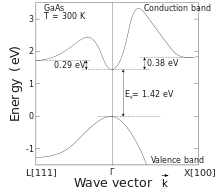
| Band gap | 1.441 eV (at 300 K)[2] |
| Electron mobility | 9000 cm2/(V·s) (at 300 K)[2] |
| -16.2×10⁻⁶ cgs[3] | |
| Thermal conductivity | 0.56 W/(cm·K) (at 300 K)[4] |
Refractive index (nD) |
3.3[3] |
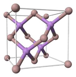
| Structure[4] | |
| Zinc blende | |
| T2d-F-43m | |
a = 565.315 pm | |
| Tetrahedral | |
| Linear | |
| Hazards | |
| Safety data sheet | External MSDS |
| GHS pictograms | 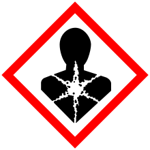 |
| GHS Signal word | Danger |
GHS hazard statements |
H350, H372, H360F |
| P261, P273, P301+310, P311, P501 | |
| NFPA 704 (fire diamond) | |
| Related compounds | |
Other anions |
Gallium nitride Gallium phosphide Gallium antimonide |
Except where otherwise noted, data are given for materials in their standard state (at 25 °C [77 °F], 100 kPa). | |
| Infobox references | |

Gallium arsenide is used in the manufacture of devices such as microwave frequency integrated circuits, monolithic microwave integrated circuits, infrared light-emitting diodes, laser diodes, solar cells and optical windows.[5]
GaAs is often used as a substrate material for the epitaxial growth of other III-V semiconductors, including indium gallium arsenide, aluminum gallium arsenide and others.
Preparation and chemistry
In the compound, gallium has a +3 oxidation state. Gallium arsenide single crystals can be prepared by three industrial processes:[5]
- The vertical gradient freeze (VGF) process (most GaAs wafers are produced using this process).[6]
- Crystal growth using a horizontal zone furnace in the Bridgman-Stockbarger technique, in which gallium and arsenic vapors react, and free molecules deposit on a seed crystal at the cooler end of the furnace.
- Liquid encapsulated Czochralski (LEC) growth is used for producing high-purity single crystals that can exhibit semi-insulating characteristics (see below).
Alternative methods for producing films of GaAs include:[5][7]
- VPE reaction of gaseous gallium metal and arsenic trichloride: 2 Ga + 2 AsCl
3 → 2 GaAs + 3 Cl
2 - MOCVD reaction of trimethylgallium and arsine: Ga(CH
3)
3 + AsH
3 → GaAs + 3 CH
4 - Molecular beam epitaxy (MBE) of gallium and arsenic: 4 Ga + As
4 → 4 GaAs or 2 Ga + As
2 → 2 GaAs
Oxidation of GaAs occurs in air, degrading performance of the semiconductor. The surface can be passivated by depositing a cubic gallium(II) sulfide layer using a tert-butyl gallium sulfide compound such as (t
BuGaS)
7.[8]
Semi-insulating crystals
In the presence of excess arsenic, GaAs boules grow with crystallographic defects; specifically, arsenic antisite defects (an arsenic atom at a gallium atom site within the crystal lattice). The electronic properties of these defects (interacting with others) cause the Fermi level to be pinned to near the center of the band gap, so that this GaAs crystal has very low concentration of electrons and holes. This low carrier concentration is similar to an intrinsic (perfectly undoped) crystal, but much easier to achieve in practice. These crystals are called "semi-insulating", reflecting their high resistivity of 107–109 Ω·cm (which is quite high for a semiconductor, but still much lower than a true insulator like glass).[9]
Etching
Wet etching of GaAs industrially uses an oxidizing agent such as hydrogen peroxide or bromine water,[10] and the same strategy has been described in a patent relating to processing scrap components containing GaAs where the Ga3+
is complexed with a hydroxamic acid ("HA"), for example:[11]
- GaAs + H
2O
2 + "HA" → "GaA" complex + H
3AsO
4 + 4 H
2O
This reaction produces arsenic acid.[12]
Electronics
GaAs digital logic
GaAs can be used for various transistor types:[13]
- Metal–semiconductor field-effect transistor (MESFET)
- High-electron-mobility transistor (HEMT)
- Junction field-effect transistor (JFET)
- Heterojunction bipolar transistor (HBT)
- Metal–oxide–semiconductor field-effect transistor (MOSFET)[14]
The HBT can be used in integrated injection logic (I2L). The earliest GaAs logic gate used Buffered FET Logic (BFL).[13]
From ~1975 to 1995 the main logic families used were:[13]
- Source-coupled FET logic (SCFL) fastest and most complex, (used by TriQuint & Vitesse)
- Capacitor–diode FET logic (CDFL) (used by Cray)
- Direct-coupled FET logic (DCFL) simplest and lowest power (used by Vitesse for VLSI gate arrays)
Comparison with silicon for electronics
GaAs advantages
Some electronic properties of gallium arsenide are superior to those of silicon. It has a higher saturated electron velocity and higher electron mobility, allowing gallium arsenide transistors to function at frequencies in excess of 250 GHz. GaAs devices are relatively insensitive to overheating, owing to their wider energy band gap, and they also tend to create less noise (disturbance in an electrical signal) in electronic circuits than silicon devices, especially at high frequencies. This is a result of higher carrier mobilities and lower resistive device parasitics. These superior properties are compelling reasons to use GaAs circuitry in mobile phones, satellite communications, microwave point-to-point links and higher frequency radar systems. It is also used in the manufacture of Gunn diodes for the generation of microwaves.
Another advantage of GaAs is that it has a direct band gap, which means that it can be used to absorb and emit light efficiently. Silicon has an indirect band gap and so is relatively poor at emitting light.
As a wide direct band gap material with resulting resistance to radiation damage, GaAs is an excellent material for outer space electronics and optical windows in high power applications.
Because of its wide band gap, pure GaAs is highly resistive. Combined with a high dielectric constant, this property makes GaAs a very good substrate for Integrated circuits and unlike Si provides natural isolation between devices and circuits. This has made it an ideal material for monolithic microwave integrated circuits (MMICs), where active and essential passive components can readily be produced on a single slice of GaAs.
One of the first GaAs microprocessors was developed in the early 1980s by the RCA corporation and was considered for the Star Wars program of the United States Department of Defense. These processors were several times faster and several orders of magnitude more radiation resistant than their silicon counterparts, but were more expensive.[15] Other GaAs processors were implemented by the supercomputer vendors Cray Computer Corporation, Convex, and Alliant in an attempt to stay ahead of the ever-improving CMOS microprocessor. Cray eventually built one GaAs-based machine in the early 1990s, the Cray-3, but the effort was not adequately capitalized, and the company filed for bankruptcy in 1995.
Complex layered structures of gallium arsenide in combination with aluminium arsenide (AlAs) or the alloy AlxGa1−xAs can be grown using molecular beam epitaxy (MBE) or using metalorganic vapor phase epitaxy (MOVPE). Because GaAs and AlAs have almost the same lattice constant, the layers have very little induced strain, which allows them to be grown almost arbitrarily thick. This allows extremely high performance and high electron mobility HEMT transistors and other quantum well devices.
Concerns over GaAs's susceptibility to heat damage have been raised, but it has been speculated that certain manufacturers would benefit from such limitations, considering the planned obsolescence cycle that many consumer electronics are designed to follow.[16]
Silicon advantages
Silicon has three major advantages over GaAs for integrated circuit manufacture. First, silicon is abundant and cheap to process in the form of silicate minerals. The economies of scale available to the silicon industry has also hindered the adoption of GaAs.
In addition, a Si crystal has a very stable structure and can be grown to very large diameter boules and processed with very good yields. It is also a fairly good thermal conductor, thus enabling very dense packing of transistors that need to get rid of their heat of operation, all very desirable for design and manufacturing of very large ICs. Such good mechanical characteristics also make it a suitable material for the rapidly developing field of nanoelectronics. Naturally, a GaAs surface cannot withstand the high temperatures needed for diffusion; however a viable and actively pursued alternative as of the 1980s was ion implantation.[17]
The second major advantage of Si is the existence of a native oxide (silicon dioxide, SiO2), which is used as an insulator. Silicon dioxide can be incorporated onto silicon circuits easily, and such layers are adherent to the underlying silicon. SiO2 is not only a good insulator (with a band gap of 8.9 eV), but the Si-SiO2 interface can be easily engineered to have excellent electrical properties, most importantly low density of interface states. GaAs does not have a native oxide, does not easily support a stable adherent insulating layer, and does not possess the dielectric strength or surface passivating qualities of the Si-SiO2.[17]
Aluminum oxide (Al2O3) has been extensively studied as a possible gate oxide for GaAs (as well as InGaAs).
The third advantage of silicon is that it possesses a higher hole mobility compared to GaAs (500 versus 400 cm2V−1s−1).[18] This high mobility allows the fabrication of higher-speed P-channel field effect transistors, which are required for CMOS logic. Because they lack a fast CMOS structure, GaAs circuits must use logic styles which have much higher power consumption; this has made GaAs logic circuits unable to compete with silicon logic circuits.
For manufacturing solar cells, silicon has relatively low absorptivity for sunlight, meaning about 100 micrometers of Si is needed to absorb most sunlight. Such a layer is relatively robust and easy to handle. In contrast, the absorptivity of GaAs is so high that only a few micrometers of thickness are needed to absorb all of the light. Consequently, GaAs thin films must be supported on a substrate material.[19]
Silicon is a pure element, avoiding the problems of stoichiometric imbalance and thermal unmixing of GaAs.
Silicon has a nearly perfect lattice; impurity density is very low and allows very small structures to be built (currently down to 16 nm[20]). In contrast, GaAs has a very high impurity density, which makes it difficult to build integrated circuits with small structures, so the 500 nm process is a common process for GaAs.
Other applications
Transistor uses
Gallium arsenide (GaAs) transistors are used for cell phones and wireless communicating. Cell phones have power amplifiers which allow the phone to send messages.[21]
Solar cells and detectors
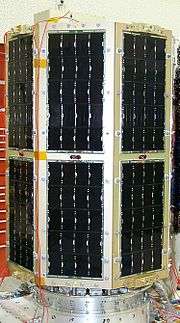
Gallium arsenide is an important semiconductor material for high-cost, high-efficiency solar cells and is used for single-crystalline thin film solar cells and for multi-junction solar cells.[22]
The first known operational use of GaAs solar cells in space was for the Venera 3 mission, launched in 1965. The GaAs solar cells, manufactured by Kvant, were chosen because of their higher performance in high temperature environments.[23] GaAs cells were then used for the Lunokhod rovers for the same reason.
In 1970, the GaAs heterostructure solar cells were developed by the team led by Zhores Alferov in the USSR,[24][25][26] achieving much higher efficiencies. In the early 1980s, the efficiency of the best GaAs solar cells surpassed that of conventional, crystalline silicon-based solar cells. In the 1990s, GaAs solar cells took over from silicon as the cell type most commonly used for photovoltaic arrays for satellite applications. Later, dual- and triple-junction solar cells based on GaAs with germanium and indium gallium phosphide layers were developed as the basis of a triple-junction solar cell, which held a record efficiency of over 32 % and can operate also with light as concentrated as 2,000 suns. This kind of solar cell powered the Mars Exploration Rovers Spirit and Opportunity, which explored Mars' surface. Also many solar cars utilize GaAs in solar arrays.
GaAs-based devices hold the world record for the highest-efficiency single-junction solar cell at 29.1 % (as of 2019). This high efficiency is attributed to the extreme high quality GaAs epitaxial growth, surface passivation by the AlGaAs,[27] and the promotion of photon recycling by the thin film design.[28]
Complex designs of AlxGa1−xAs-GaAs devices using quantum wells can be sensitive to infrared radiation (QWIP).
GaAs diodes can be used for the detection of X-rays.[29]
Light-emission devices
GaAs has been used to produce near-infrared laser diodes since 1962.[30] It is often used in alloys with other semiconductor compounds for these applications.
Fiber optic temperature measurement
For this purpose an optical fiber tip of an optical fiber temperature sensor is equipped with a gallium arsenide crystal. Starting at a light wavelength of 850 nm GaAs becomes optically translucent. Since the spectral position of the band gap is temperature dependent, it shifts about 0.4 nm/K. The measurement device contains a light source and a device for the spectral detection of the band gap. With the changing of the band gap, (0.4 nm/K) an algorithm calculates the temperature (all 250 ms).[31]
Spin-charge converters
GaAs may have applications in spintronics as it can be used instead of platinum in spin-charge converters and may be more tunable.[32]
Safety
The environment, health and safety aspects of gallium arsenide sources (such as trimethylgallium and arsine) and industrial hygiene monitoring studies of metalorganic precursors have been reported.[33] California lists gallium arsenide as a carcinogen,[34] as do IARC and ECA,[35] and it is considered a known carcinogen in animals.[36][37] On the other hand, a 2013 review (funded by industry) argued against these classifications, saying that when rats or mice inhale fine GaAs powders (as in previous studies), they get cancer from the resulting lung irritation and inflammation, rather than from a primary carcinogenic effect of the GaAs itself—and that, moreover, fine GaAs powders are unlikely to be created in the production or use of GaAs.[35]
See also
- Aluminium arsenide
- Aluminium gallium arsenide
- Arsine
- Cadmium telluride
- Gallium antimonide
- Gallium arsenide phosphide
- Gallium manganese arsenide
- Gallium nitride
- Gallium phosphide
- Heterostructure emitter bipolar transistor
- Indium arsenide
- Indium gallium arsenide
- Indium phosphide
- Light-emitting diode
- MESFET (metal–semiconductor field-effect transistor)
- MOVPE
- Multijunction solar cell
- Photomixing to generate THz
- Trimethylgallium
References
- Haynes, p. 4.64
- Haynes, p. 12.90
- Haynes, p. 12.86
- Haynes, p. 12.81
- Moss, S. J.; Ledwith, A. (1987). The Chemistry of the Semiconductor Industry. Springer. ISBN 978-0-216-92005-7.
- Scheel, Hans J.; Tsuguo Fukuda. (2003). Crystal Growth Technology. Wiley. ISBN 978-0471490593.
- Smart, Lesley; Moore, Elaine A. (2005). Solid State Chemistry: An Introduction. CRC Press. ISBN 978-0-7487-7516-3.
- "Chemical vapor deposition from single organometallic precursors" A. R. Barron, M. B. Power, A. N. MacInnes, A. F.Hepp, P. P. Jenkins U.S. Patent 5,300,320 (1994)
- McCluskey, Matthew D. and Haller, Eugene E. (2012) Dopants and Defects in Semiconductors, pp. 41 and 66, ISBN 978-1439831526
- Brozel, M. R.; Stillman, G. E. (1996). Properties of Gallium Arsenide. IEEE Inspec. ISBN 978-0-85296-885-7.
- "Oxidative dissolution of gallium arsenide and separation of gallium from arsenic" J. P. Coleman and B. F. Monzyk U.S. Patent 4,759,917 (1988)
- Lova, Paola; Robbiano, Valentina; Cacialli, Franco; Comoretto, Davide; Soci, Cesare (3 October 2018). "Black GaAs by Metal-Assisted Chemical Etching". ACS Applied Materials & Interfaces. 10 (39): 33434–33440. doi:10.1021/acsami.8b10370. ISSN 1944-8244. PMID 30191706.
- Dennis Fisher; I. J. Bahl (1995). Gallium Arsenide IC Applications Handbook. 1. Elsevier. p. 61. ISBN 978-0-12-257735-2. 'Clear search' to see pages
- Ye, Peide D.; Xuan, Yi; Wu, Yanqing; Xu, Min (2010). "Atomic-Layer Deposited High-k/III-V Metal-Oxide-Semiconductor Devices and Correlated Empirical Model". In Oktyabrsky, Serge; Ye, Peide (eds.). Fundamentals of III-V Semiconductor MOSFETs. Springer Science & Business Media. pp. 173–194. doi:10.1007/978-1-4419-1547-4_7. ISBN 978-1-4419-1547-4.
- Šilc, Von Jurij; Robič, Borut; Ungerer, Theo (1999). Processor architecture: from dataflow to superscalar and beyond. Springer. p. 34. ISBN 978-3-540-64798-0.
- "A reprieve for Moore's Law: milspec chip writes computing's next chapter". Ars Technica. 2016-06-09. Retrieved 2016-06-14.
- Morgan, D. V.; Board, K. (1991). An Introduction To Semiconductor Microtechnology (2nd ed.). Chichester, West Sussex, England: John Wiley & Sons. p. 137. ISBN 978-0471924784.
- Sze, S. M. (1985). Semiconductor Devices Physics and Technology. John Wiley & Sons. Appendix G. ISBN 0-471-87424-8
- Single-Crystalline Thin Film. US Department of Energy
- Handy, Jim (17 July 2013) Micron NAND Reaches 16nm. thememoryguy.com
- . 15 December, 2010. Text "https://seekingalpha.com/article/242049-its-a-gaas-critical-component-for-cell-phone-circuits-grows-in-2010 " ignored (help); Check date values in:
|date=(help); Missing or empty|title=(help) - Yin, Jun; Migas, Dmitri B.; Panahandeh-Fard, Majid; Chen, Shi; Wang, Zilong; Lova, Paola; Soci, Cesare (3 October 2013). "Charge Redistribution at GaAs/P3HT Heterointerfaces with Different Surface Polarity". The Journal of Physical Chemistry Letters. 4 (19): 3303–3309. doi:10.1021/jz401485t.
- Strobl, G.F.X.; LaRoche, G.; Rasch, K.-D.; Hey, G. (2009). "2: From Extraterrestrial to Terrestrial Applications". High-Efficient Low-Cost Photovoltaics: Recent Developments. Springer. doi:10.1007/978-3-540-79359-5. ISBN 978-3-540-79359-5.
- Alferov, Zh. I., V. M. Andreev, M. B. Kagan, I. I. Protasov and V. G. Trofim, 1970, ‘‘Solar-energy converters based on p-n AlxGa1−xAs-GaAs heterojunctions,’’ Fiz. Tekh. Poluprovodn. 4, 2378 (Sov. Phys. Semicond. 4, 2047 (1971))
- Nanotechnology in energy applications. im.isu.edu.tw. 16 November 2005 (in Chinese) p. 24
- Nobel Lecture by Zhores Alferov at nobelprize.org, p. 6
- Schnitzer, I.; et al. (1993). "Ultrahigh spontaneous emission quantum efficiency, 99.7 % internally and 72 % externally, from AlGaAs/GaAs/AlGaAs double heterostructures". Applied Physics Letters. 62 (2): 131. Bibcode:1993ApPhL..62..131S. doi:10.1063/1.109348. S2CID 14611939.
- Wang, X.; et al. (2013). "Design of GaAs Solar Cells Operating Close to the Shockley–Queisser Limit". IEEE Journal of Photovoltaics. 3 (2): 737. doi:10.1109/JPHOTOV.2013.2241594.
- Glasgow University report on CERN detector. Ppewww.physics.gla.ac.uk. Retrieved on 2013-10-16.
- Hall, Robert N.; Fenner, G. E.; Kingsley, J. D.; Soltys, T. J. and Carlson, R. O. (1962). "Coherent Light Emission From GaAs Junctions". Physical Review Letters. 9 (9): 366–369. Bibcode:1962PhRvL...9..366H. doi:10.1103/PhysRevLett.9.366.CS1 maint: multiple names: authors list (link)
- A New Fiber Optical Thermometer and Its Application for Process Control in Strong Electric, Magnetic, and Electromagnetic Fields. optocon.de (PDF; 2,5 MB)
- GaAs forms basis of tunable spintronics. compoundsemiconductor.net. September 2014
- Shenai-Khatkhate, D V; Goyette, R; DiCarlo, R L; Dripps, G (2004). "Environment, health and safety issues for sources used in MOVPE growth of compound semiconductors". Journal of Crystal Growth. 272 (1–4): 816–821. Bibcode:2004JCrGr.272..816S. doi:10.1016/j.jcrysgro.2004.09.007.
- "Chemicals Listed Effective August 1, 2008 as Known to the State of California to Cause Cancer or Reproductive Toxicity: gallium arsenide, hexafluoroacetone, nitrous oxide and vinyl cyclohexene dioxide". OEHHA. 2008-08-01.
- Bomhard, E. M.; Gelbke, H.; Schenk, H.; Williams, G. M.; Cohen, S. M. (2013). "Evaluation of the carcinogenicity of gallium arsenide". Critical Reviews in Toxicology. 43 (5): 436–466. doi:10.3109/10408444.2013.792329. PMID 23706044.
- "NTP Technical Report On The Toxicology And Carcinogenesis Studies Of Gallium Arsenide (Cas No. 1303-00-0) In F344/N Rats And B6c3f1 Mice (Inhalation Studies)" (PDF). U.S. Department Of Health And Human Services: Public Health Service: National Institutes of Health. September 2000.
- "Safety Data Sheet: Gallium Arsenide". Sigma-Aldrich. 2015-02-28.
Cited sources
- Haynes, William M., ed. (2011). CRC Handbook of Chemistry and Physics (92nd ed.). CRC Press. ISBN 978-1439855119.
External links
| Wikimedia Commons has media related to Gallium arsenide. |
- Case Studies in Environmental Medicine: Arsenic Toxicity
- Physical properties of gallium arsenide (Ioffe Institute)
- Facts and figures on processing gallium arsenide
| Authority control |
|
|---|
| Basic types |
|
|---|---|
| Hybrid types |
|
| Other Types | |
| Theory | |
| Materials |
|
| |