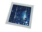
Crystalline silicon
Crystalline silicon (c-Si) is the crystalline forms of silicon, either polycrystalline silicon (poly-Si, consisting of small crystals), or monocrystalline silicon (mono-Si, a continuous crystal). Crystalline silicon is the dominant semiconducting material used in photovoltaic technology for the production of solar cells. These cells are assembled into solar panels as part of a photovoltaic system to generate solar power from sunlight.
In electronics, crystalline silicon is typically the monocrystalline form of silicon, and is used for producing microchips. This silicon contains much lower impurity levels than those required for solar cells. Production of semiconductor grade silicon involves a chemical purification to produce hyperpure polysilicon followed by a recrystallization process to grow monocrystalline silicon. The cylindrical boules are then cut into wafers for further processing.
Solar cells made of crystalline silicon are often called conventional, traditional, or first generation solar cells, as they were developed in the 1950s and remained the most common type up to the present time.[1][2] Because they are produced from 160–190 μm thick solar wafers—slices from bulks of solar grade silicon—they are sometimes called wafer-based solar cells.
Solar cells made from c-Si are single-junction cells and are generally more efficient than their rival technologies, which are the second-generation thin-film solar cells, the most important being CdTe, CIGS, and amorphous silicon (a-Si). Amorphous silicon is an allotropic variant of silicon, and amorphous means "without shape" to describe its non-crystalline form.[3]:29
Overview
Classification
The allotropic forms of silicon range from a single crystalline structure to a completely unordered amorphous structure with several intermediate varieties. In addition, each of these different forms can possess several names and even more abbreviations, and often cause confusion to non-experts, especially as some materials and their application as a PV technology are of minor significance, while other materials are of outstanding importance.
PV industry
The photovoltaic industry, however, groups them into two distinct categories:
- crystalline silicon (c-Si), used in traditional, conventional, wafer-based solar cells:
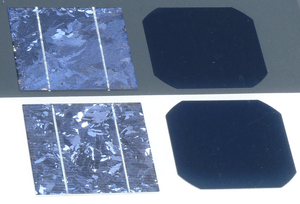
- monocrystalline silicon (mono-Si)
- polycrystalline silicon (multi-Si)
- ribbon silicon (ribbon-Si), has currently no market[3]:17,18
- not classified as crystalline silicon, used in thin-film and other solar-cell technologies:
- amorphous silicon (a-Si)
- nanocrystalline silicon (nc-Si)
- protocrystalline silicon (pc-Si)
- other non-silicon materials, such as CdTe, CIGS
- emerging photovoltaics
- multi-junction solar cells (MJ) commonly used for solar panels on spacecrafts for space-based solar power. They are also used in concentrator photovoltaics (CPV, HCPV), an emerging technology best suited for locations that receive much sunlight.
Generations
Alternatively, different types of solar cells and/or their semiconducting materials can be classified by generations:
- First generation solar cells are made of crystalline silicon, also called, conventional, traditional, wafer-based solar cells and include monocrystalline (mono-Si) and polycrystalline (multi-Si) semiconducting materials.
- Second generation solar cells or panels are based on thin-film technology and are of commercially significant importance. These include CdTe, CIGS and amorphous silicon.
- Third generation solar cells are often labeled as emerging technologies with little or no market significance and include a large range of substances, mostly organic, often using organometallic compounds.
Arguably, multi-junction photovoltaic cells can be classified to neither of these generations. A typical triple junction semiconductor is made of InGaP/(In)GaAs/Ge.[4][5]
Comparison of technical specifications
| Categories | Technology | η (%) | VOC (V) | ISC (A) | W/m² | t (μm) |
|---|---|---|---|---|---|---|
| Thin-film solar cells |
a-Si | 11.1 | 6.3 | 0.0089 | 33 | 1 |
| CdTe | 16.5 | 0.86 | 0.029 | – | 5 | |
| CIGS | 20.5 | – | – | – | ||
Market share
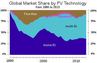
In 2013, conventional crystalline silicon technology dominated worldwide PV production, with multi-Si leading the market ahead of mono-Si, accounting for 54 percent and 36 percent, respectively. For the last ten years, worldwide market-share of thin-film technologies stagnated below 18 percent and currently stand at 9 percent. In the thin-film market, CdTe leads with an annual production of 2 GWp or 5 percent, followed by a-Si and CIGS, both around 2 percent.[3]:4,18 Alltime deployed PV capacity of 139 gigawatts (cumulative as of 2013) splits up into 121 GW crystalline silicon (87%) and 18 GW thin-film (13%) technology.[3]:41
Efficiency
The conversion efficiency of PV devices describes the energy-ratio of the outgoing electrical power compared to the incoming radiated light. A single solar cells has generally a better, or higher efficiency than an entire solar module. Also lab efficiency is always significantly ahead of commercially available products in the market.
- Lab cells
In 2013, record lab cell efficiency was highest for crystalline silicon. However, multi-silicon is followed closely by Cadmium Telluride and Copper indium gallium selenide solar cells
- 25.6% – mono-Si cell
- 20.4% – multi-Si cell
- 21.7% – CIGS cell
- 21.5% – CdTe cell
These are all single-junction solar cells. For high concentration, multi-junction cells the record as of 2014 stood at 44.7 percent.[3]:6
- Modules
The average commercial crystalline silicon module increased its efficiency from about 12 to 16 percent over the last ten years. In the same period CdTe-modules improved their efficiency from 9 to 16 percent. The modules performing best under lab conditions in 2014 were made of monocrystalline silicon. They were 7 percentage points above the efficiency of commercially produced modules (23% vs 16%) which indicated that the conventional silicon technology still had potential to improve and therefore maintain its leading position.[3]:6
The best lab module efficiencies for multi-junction modules with concentrator technology in 2014 reached 36.7 percent efficiency.[3]:6
Energy payback time
The energy payback time (EPBT) describes the time span a PV system needs to operate in order to generate the same amount of energy that was used for its manufacture and installation. This energy amortization, given in years, is also referred to as break-even energy payback time.[6] The EPBT depends vastly on the location where the PV system is installed (e.g. the amount of sunlight available) and on the efficiency of the system, namely the type of PV technology and the system's components.
In life-cycle analysis (LCA) from the 1990s, the energy payback time had often been cited to be as high as 10 years.[7] Although the time span already decreased to less than 3 years in the early 2000s,[8] the myth that "solar PV does not pay back the energy used to create it" seems to persist up to the present day.[9]
The EPBT relates closely to the concepts of net energy gain (NEG) and energy returned on energy invested (EROI). They are both used in energy economics and refer to the difference between the energy expended to harvest an energy source and the amount of energy gained from that harvest. The NEG and EROI also take the operating lifetime of a PV system into account and an effective production life of 25 to 30 years is typically assumed, as many manufacturers now provide a 25-year warranty on their products. From these metrics, the Energy payback Time can be derived by calculation.[10][11]
| Exemplary locations | Crystalline silicon | Thin-film | CPV | Radiation map color |
Global solar irradiance in kWh/m² | |||
|---|---|---|---|---|---|---|---|---|
| mono | poly | a-Si | CIGS | CdTe | ||||
| North and Central Europe, Canada | 3.3 | 2.1 | 2.4 | 1.7 | 1.1 | – | 1200 kWh | 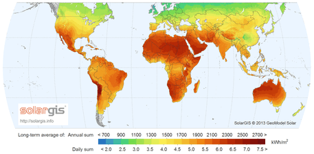 |
| Southern Europe, USA, South America, India | 1.8 | 1.2 | 1.3 | 0.9 | 0.7 | 0.8 | 1700 kWh | |
| American Southwest, Australia, Africa, Middle East | 1.5 | <1.2 | 0.9 | <0.9 | <0.7 | <0.8 | 1900 kWh | |
| Source: Fraunhofer FHI, Energy Payback Time, presentation slides, and photovolatic report, p. 34–35[12] and references given therein. The payback times have been substantially reduced since 2011. Table: kWh/m²/a - kilowatt-hours per square metre per year, as Global Horizontal Irradiation | ||||||||
- EPBT improvements
The EPBT has always been longer for PV systems using crystalline silicon than thin-film technology. This is due to the fact that silicon is produced by the reduction of high-grade quartz sand in electric furnaces. This carbo-thermic smelting process occurs at high temperatures of more than 1000 °C and is very energy intensive, using about 11 kilowatt-hours (kWh) per produced kilogram of silicon.[13] However, the energy payback time has shortened significantly over the last years, as crystalline silicon cells became ever more efficient in converting sunlight, while the thickness of the wafer material was constantly reduced and therefore required less silicon for its manufacture. Within the last ten years, the amount of silicon used for solar cells declined from 16 to 6 grams per watt-peak. In the same period, the thickness of a c-Si wafer was reduced from 300 μm, or microns, to about 160–190 μm. Crystalline silicon wafers are nowadays only 40 percent as thick as they used to be in 1990, when they were around 400 μm.[3]:29 The sawing techniques that slice crystalline silicon ingots into wafers have also improved by reducing the kerf loss and making it easier to recycle the silicon sawdust.[14][15]
| Parameter | Mono-Si | CdTe |
|---|---|---|
| Cell efficiency | 16.5% | 15.6% |
| Derate cell to module efficiency | 8.5% | 13.9% |
| Module efficiency | 15.1% | 13.4% |
| Wafer thickness / layer thickness | 190 μm | 4.0 μm |
| Kerf loss | 190 μm | – |
| Silver per cell | 9.6 g/m2 | – |
| Glass thickness | 4.0 mm | 3.5 mm |
| Operational lifetime | 30 years | 30 years |
| Source: IEA-PVPS, Life Cycle Assessment, March 2015[16] | ||
Toxicity
With the exception of amorphous silicon, most commercially established PV technologies use toxic heavy metals. CIGS often uses a CdS buffer layer, and the semiconductor material of CdTe-technology itself contains the toxic cadmium (Cd). In the case of crystalline silicon modules, the solder material that joins together the copper strings of the cells, it contains about 36 percent of lead (Pb). Moreover, the paste used for screen printing front and back contacts contains traces of Pb and sometimes Cd as well. It is estimated that about 1,000 metric tonnes of Pb have been used for 100 gigawatts of c-Si solar modules. However, there is no fundamental need for lead in the solder alloy.[17]
Cell technologies
PERC solar cell
Passivated emitter rear contact (PERC) solar cells [18] consist of the addition of an extra layer to the rear-side of a solar cell. This dielectric passive layer acts to reflect unabsorbed light back to the solar cell for a second absorption attempt increasing the solar cell efficiency.[19]
A PERC is created through an additional film deposition and etching process. Etching can be done either by chemical or laser processing.
HIT solar cell

A HIT solar cell is composed of a mono thin crystalline silicon wafer surrounded by ultra-thin amorphous silicon layers.[20] The acronym HIT stands for "heterojunction with intrinsic thin layer". HIT cells are produced by the Japanese multinational electronics corporation Panasonic (see also Sanyo § Solar cells and plants).[21] Panasonic and several other groups have reported several advantages of the HIT design over its traditional c-Si counterpart:
1. An intrinsic a-Si layer can act as an effective surface passivation layer for c-Si wafer.
2. The p+/n+ doped a-Si functions as an effective emitter/BSF for the cell.
3. The a-Si layers are deposited at much lower temperature, compared to the processing temperatures for traditional diffused c-Si technology.
4. The HIT cell has a lower temperature coefficient compared to c-Si cell technology.
Owing to all these advantages, this new hetero-junction solar cell is a considered to be a promising low cost alternative to traditional c-Si based solar cells.
Fabrication of HIT cells
The details of the fabrication sequence vary from group to group. Typically, good quality, CZ/FZ grown c-Si wafer (with ~1ms lifetimes) are used as the absorber layer of HIT cells. Using alkaline etchants, such as, NaOH or (CH3)4NOH the (100) surface of the wafer is textured to form the pyramids of 5-10μm height. Next, the wafer is cleaned using peroxide and HF solutions. This is followed by deposition of intrinsic a-Si passivation layer, typically through PECVD or Hot-wire CVD.[22][23] The silane (SiH4) gas diluted with H2 is used as a precursor. The deposition temperature and pressure is maintained at 200o C and 0.1-1 Torr. Precise control over this step is essential to avoid the formation of defective epitaxial Si.[24] Cycles of deposition and annealing and H2 plasma treatment are shown to have provided excellent surface passivation.[25][26] Diborane or Trimethylboron gas mixed with SiH4 is used to deposit p-type a-Si layer, while, Phosphine gas mixed with SiH4 is used to deposit n-type a-Si layer. Direct deposition of doped a-Si layers on c-Si wafer is shown to have very poor passivation properties.[27] This is most likely due to dopant induced defect generation in a-Si layers.[28] Sputtered Indium Tin Oxide (ITO) is commonly used as a transparent conductive oxide (TCO) layer on top of the front and back a-Si layer in bi-facial design, as a-Si has high lateral resistance. It is generally deposited on the back side as well fully metallized cell to avoid diffusion of back metal and also for impedance matching for the reflected light.[29] The silver/aluminum grid of 50-100μm thick is deposited through stencil printing for the front contact and back contact for bi-facial design. The detailed description of the fabrication process can be found in.[30]
Opto-Electrical Modeling and Characterization of HIT Cells
The literature discusses several studies to interpret carrier transport bottlenecks in these cells. Traditional light and dark I-V are extensively studied [31][32][33] and are observed to have several non-trivial features, which cannot be explained using the traditional solar cell diode theory.[34] This is because of the presence of hetero-junction between the intrinsic a-Si layer and c-Si wafer which introduces additional complexities to current flow.[31][35] In addition, there has been significant efforts to characterize this solar cell using C-V,[36][37] impedance spectroscopy,[36][38][39] surface photo-voltage,[40] suns-Voc[41][42] to produce complementary information.
Further, a number of design improvements, such as, the use of new emitters,[43] bifacial configuration, interdigitated back contact (IBC) configuration[44] bifacial-tandem configuration[45] are actively being pursued.
Mono-silicon

Monocrystalline silicon (mono c-Si) is a form in which the crystal structure is homogeneous throughout the material; the orientation, lattice parameter, and electronic properties are constant throughout the material.[46] Dopant atoms such as phosphorus and boron are often incorporated into the film to make the silicon n-type or p-type respectively. Monocrystalline silicon is fabricated in the form of silicon wafers, usually by the Czochralski Growth method, and can be quite expensive depending on the radial size of the desired single crystal wafer (around $200 for a 300 mm Si wafer).[46] This monocrystalline material, while useful, is one of the chief expenses associated with producing photovoltaics where approximately 40% of the final price of the product is attributable to the cost of the starting silicon wafer used in cell fabrication.[47]
Polycrystalline silicon
Polycrystalline silicon is composed of many smaller silicon grains of varied crystallographic orientation, typically >1 mm in size. This material can be synthesized easily by allowing liquid silicon to cool using a seed crystal of the desired crystal structure. Additionally, other methods for forming smaller-grained polycrystalline silicon (poly-Si) exist such as high temperature chemical vapor deposition (CVD).
Not classified as crystalline silicon
These allotropic forms of silicon are not classified as crystalline silicon. They belong to the group of thin-film solar cells.
Amorphous silicon
Amorphous silicon (a-Si) has no long-range periodic order. The application of amorphous silicon to photovoltaics as a standalone material is somewhat limited by its inferior electronic properties.[48] When paired with microcrystalline silicon in tandem and triple-junction solar cells, however, higher efficiency can be attained than with single-junction solar cells.[49] This tandem assembly of solar cells allows one to obtain a thin-film material with a bandgap of around 1.12 eV (the same as single-crystal silicon) compared to the bandgap of amorphous silicon of 1.7-1.8 eV bandgap. Tandem solar cells are then attractive since they can be fabricated with a bandgap similar to single-crystal silicon but with the ease of amorphous silicon.
Nanocrystalline silicon
Nanocrystalline silicon (nc-Si), sometimes also known as microcrystalline silicon (μc-Si), is a form of porous silicon.[50] It is an allotropic form of silicon with paracrystalline structure—is similar to amorphous silicon (a-Si), in that it has an amorphous phase. Where they differ, however, is that nc-Si has small grains of crystalline silicon within the amorphous phase. This is in contrast to polycrystalline silicon (poly-Si) which consists solely of crystalline silicon grains, separated by grain boundaries. The difference comes solely from the grain size of the crystalline grains. Most materials with grains in the micrometre range are actually fine-grained polysilicon, so nanocrystalline silicon is a better term. The term Nanocrystalline silicon refers to a range of materials around the transition region from amorphous to microcrystalline phase in the silicon thin film.
Protocrystalline silicon
Protocrystalline silicon has a higher efficiency than amorphous silicon (a-Si) and it has also been shown to improve stability, but not eliminate it.[51][52] A protocrystalline phase is a distinct phase occurring during crystal growth which evolves into a microcrystalline form.
Protocrystalline Si also has a relatively low absorption near the band gap owing to its more ordered crystalline structure. Thus, protocrystalline and amorphous silicon can be combined in a tandem solar cell where the top layer of thin protocrystalline silicon absorbs short-wavelength light whereas the longer wavelengths are absorbed by the underlying a-Si substrate.
Transformation of amorphous into crystalline silicon
Amorphous silicon can be transformed to crystalline silicon using well-understood and widely implemented high-temperature annealing processes. The typical method used in industry requires high-temperature compatible materials, such as special high temperature glass that is expensive to produce. However, there are many applications for which this is an inherently unattractive production method.
Low temperature induced crystallization
Flexible solar cells have been a topic of interest for less conspicuous-integrated power generation than solar power farms. These modules may be placed in areas where traditional cells would not be feasible, such as wrapped around a telephone pole or cell phone tower. In this application a photovoltaic material may be applied to a flexible substrate, often a polymer. Such substrates cannot survive the high temperatures experienced during traditional annealing. Instead, novel methods of crystallizing the silicon without disturbing the underlying substrate have been studied extensively. Aluminum-induced crystallization (AIC) and local laser crystallization are common in the literature, however not extensively used in industry.
In both of these methods, amorphous silicon is grown using traditional techniques such as plasma-enhanced chemical vapor deposition (PECVD). The crystallization methods diverge during post-deposition processing.
In aluminum-induced crystallization, a thin layer of aluminum (50 nm or less) is deposited by physical vapor deposition onto the surface of the amorphous silicon. This stack of material is then annealed at a relatively low temperature between 140 °C and 200 °C in a vacuum. The aluminum that diffuses into the amorphous silicon is believed to weaken the hydrogen bonds present, allowing crystal nucleation and growth.[53] Experiments have shown that polycrystalline silicon with grains on the order of 0.2 – 0.3 μm can be produced at temperatures as low as 150 °C. The volume fraction of the film that is crystallized is dependent on the length of the annealing process.[53]
Aluminum-induced crystallization produces polycrystalline silicon with suitable crystallographic and electronic properties that make it a candidate for producing polycrystalline thin films for photovoltaics.[53] AIC can be used to generate crystalline silicon nanowires and other nano-scale structures.
Another method of achieving the same result is the use of a laser to heat the silicon locally without heating the underlying substrate beyond some upper temperature limit. An excimer laser or, alternatively, green lasers such as a frequency-doubled Nd:YAG laser is used to heat the amorphous silicon, supplying energy necessary to nucleate grain growth. The laser fluence must be carefully controlled in order to induce crystallization without causing widespread melting. Crystallization of the film occurs as a very small portion of the silicon film is melted and allowed to cool. Ideally, the laser should melt the silicon film through its entire thickness, but not damage the substrate. Toward this end, a layer of silicon dioxide is sometimes added to act as a thermal barrier.[54] This allows the use of substrates that cannot be exposed to the high temperatures of standard annealing, polymers for instance. Polymer-backed solar cells are of interest for seamlessly integrated power production schemes that involve placing photovoltaics on everyday surfaces.
A third method for crystallizing amorphous silicon is the use of thermal plasma jet. This strategy is an attempt to alleviate some of the problems associated with laser processing – namely the small region of crystallization and the high cost of the process on a production scale. The plasma torch is a simple piece of equipment that is used to thermally anneal the amorphous silicon. Compared to the laser method, this technique is simpler and more cost effective.[55]
Plasma torch annealing is attractive because the process parameters and equipment dimension can be changed easily to yield varying levels of performance. A high level of crystallization (~90%) can be obtained with this method. Disadvantages include difficulty achieving uniformity in the crystallization of the film. While this method is applied frequently to silicon on a glass substrate, processing temperatures may be too high for polymers.
See also
References
- "Bell Labs Demonstrates the First Practical Silicon Solar Cell". aps.org.
- D. M. Chapin-C. S. Fuller-G. L. Pearson (1954). "A New Silicon p–n Junction Photocell for Converting Solar Radiation into Electrical Power". Journal of Applied Physics. 25 (5): 676–677. Bibcode:1954JAP....25..676C. doi:10.1063/1.1721711.
- "Photovoltaics Report" (PDF). Fraunhofer ISE. 28 July 2014. Archived (PDF) from the original on 31 August 2014. Retrieved 31 August 2014.
- High-efficiency multi-junction solar cells Archived 2012-03-21 at the Wayback Machine
- "Multi-Junction Solar Cells". stanford.edu.
- Ibon Galarraga, M. González-Eguino, Anil Markandya (1 January 2011). Handbook of Sustainable Energy. Edward Elgar Publishing. p. 37. ISBN 978-0857936387. Retrieved 9 May 2017 – via Google Books.CS1 maint: multiple names: authors list (link)
- "An analysis of the energy efficiency of photovoltaic cells in reducing CO2 emmisions". University of Portsmouth. 31 May 2009. Archived from the original on 25 March 2015.
Energy Pay Back time comparison for Photovoltaic Cells (Alsema, Frankl, Kato, 1998, p. 5
- Vasilis Fthenakis and Erik Alsema (2005). "Photovoltaics Energy Payback Times, Greenhouse Gas Emissions and External Costs: 2004–early 2005 Status" (PDF). clca.columbia.edu. Archived (PDF) from the original on 25 March 2015.CS1 maint: uses authors parameter (link)
- Mark Diesendorf (16 December 2013). "Dispelling myth of energy payback of renewable energy systems". REneweconomy.com.
- Marco Raugei, Pere Fullana-i-Palmer and Vasilis Fthenakis (March 2012). "The Energy Return on Energy Investment (EROI) of Photovoltaics: Methodology and Comparisons with Fossil Fuel Life Cycles" (PDF). www.bnl.gov/. Archived (PDF) from the original on 28 March 2015.CS1 maint: uses authors parameter (link)
- Vasilis Fthenakis, Rolf Frischknecht, Marco Raugei, Hyung Chul Kim, Erik Alsema, Michael Held and Mariska de Wild-Scholten (November 2011). "Methodology Guidelines on Life Cycle Assessment of Photovoltaic Electricity" (PDF). www.iea-pvps.org/. IEA-PVPS. pp. 8–10. Archived (PDF) from the original on 28 March 2015.CS1 maint: uses authors parameter (link)
- http://www.ise.fraunhofer.de/de/downloads/pdf-files/aktuelles/photovoltaics-report-in-englischer-sprache.pdf
- "Production Process of Silicon". www.simcoa.com.au. Simcoa Operations. Archived from the original on 17 September 2014. Retrieved 17 September 2014.
- "Reaching kerf loss below 100 μm by optimizations" (PDF). Fraunhofer ISE, 24th European PV Solar Energy Conference and Exhibition. September 2009.
- "Silicon kerf loss recycling". HZDR - Helmholtz-Zentrum Dresden-Rossendorf. 4 April 2014.
- "Life Cycle Assessment of Future Photovoltaic Electricity Production from Residential-scale Systems Operated in Europe". IEA-PVPS. 13 March 2015.
- Werner, Jürgen H. (2 November 2011). "Toxic Substances In Photovoltaic Modules" (PDF). postfreemarket.net. Institute of Photovoltaics, University of Stuttgart, Germany - The 21st International Photovoltaic Science and Engineering Conference 2011 Fukuoka, Japan. p. 2. Archived from the original (PDF) on 23 September 2014. Retrieved 23 September 2014.
- "assivated emitter rear contact solar cells are at 20% efficiency today—but price premiums are steep". GreentechMedia. 14 August 2014.
- "What is PERC? Why should you care?". Solar Power World. 5 July 2016.
- http://solar.sanyo.com/hit.html
- "Why Panasonic HIT - Panasonic Solar HIT - Eco solutions - Business - Panasonic Global". panasonic.net. Retrieved 17 April 2018.
- Taguchi, Mikio; Terakawa, Akira; Maruyama, Eiji; Tanaka, Makoto (2005-09-01). "Obtaining a higher Voc in HIT cells". Progress in Photovoltaics: Research and Applications. 13 (6): 481–488. doi:10.1002/pip.646. ISSN 1099-159X.
- Wang, T.H.; Iwaniczko, E.; Page, M.R.; Levi, D.H.; Yan, Y.; Yelundur, V.; Branz, H.M.; Rohatgi, A.; Wang, Q. (2005). "Effective interfaces in silicon heterojunction solar cells". Conference Record of the Thirty-first IEEE Photovoltaic Specialists Conference, 2005. pp. 955–958. doi:10.1109/PVSC.2005.1488290. ISBN 978-0-7803-8707-2.
- Wolf, Stefaan De; Kondo, Michio (2007-01-22). "Abruptness of a-Si:H∕c-Si interface revealed by carrier lifetime measurements". Applied Physics Letters. 90 (4): 042111. Bibcode:2007ApPhL..90d2111D. doi:10.1063/1.2432297. ISSN 0003-6951.
- Mews, Mathias; Schulze, Tim F.; Mingirulli, Nicola; Korte, Lars (2013-03-25). "Hydrogen plasma treatments for passivation of amorphous-crystalline silicon-heterojunctions on surfaces promoting epitaxy". Applied Physics Letters. 102 (12): 122106. Bibcode:2013ApPhL.102l2106M. doi:10.1063/1.4798292. ISSN 0003-6951.
- Descoeudres, A.; Barraud, L.; Wolf, Stefaan De; Strahm, B.; Lachenal, D.; Guérin, C.; Holman, Z. C.; Zicarelli, F.; Demaurex, B. (2011-09-19). "Improved amorphous/crystalline silicon interface passivation by hydrogen plasma treatment". Applied Physics Letters. 99 (12): 123506. Bibcode:2011ApPhL..99l3506D. doi:10.1063/1.3641899. ISSN 0003-6951.
- Tanaka, Makoto; Taguchi, Mikio; Matsuyama, Takao; Sawada, Toru; Tsuda, Shinya; Nakano, Shoichi; Hanafusa, Hiroshi; Kuwano, Yukinori (1992-11-01). "Development of New a-Si/c-Si Heterojunction Solar Cells: ACJ-HIT (Artificially Constructed Junction-Heterojunction with Intrinsic Thin-Layer)". Japanese Journal of Applied Physics. 31 (Part 1, No. 11): 3518–3522. Bibcode:1992JaJAP..31.3518T. doi:10.1143/jjap.31.3518.
- Street, R. A.; Biegelsen, D. K.; Knights, J. C. (1981-07-15). "Defect states in doped and compensated $a$-Si: H". Physical Review B. 24 (2): 969–984. Bibcode:1981PhRvB..24..969S. doi:10.1103/PhysRevB.24.969.
- Banerjee, A.; Guha, S. (1991-01-15). "Study of back reflectors for amorphous silicon alloy solar cell application". Journal of Applied Physics. 69 (2): 1030–1035. Bibcode:1991JAP....69.1030B. doi:10.1063/1.347418. ISSN 0021-8979.
- De Wolf, Stefaan; Descoeudres, Antoine; Holman, Zachary C.; Ballif, Christophe (2012). "High-efficiency Silicon Heterojunction Solar Cells: A Review" (PDF). Green. 2 (1). doi:10.1515/green-2011-0018.
- Chavali, R.V.K.; Wilcox, J.R.; Ray, B.; Gray, J.L.; Alam, M.A. (2014-05-01). "Correlated Nonideal Effects of Dark and Light I #x2013;V Characteristics in a-Si/c-Si Heterojunction Solar Cells". IEEE Journal of Photovoltaics. 4 (3): 763–771. doi:10.1109/JPHOTOV.2014.2307171. ISSN 2156-3381.
- Matsuura, Hideharu; Okuno, Tetsuhiro; Okushi, Hideyo; Tanaka, Kazunobu (1984-02-15). "Electrical properties of n-amorphous/p-crystalline silicon heterojunctions". Journal of Applied Physics. 55 (4): 1012–1019. Bibcode:1984JAP....55.1012M. doi:10.1063/1.333193. ISSN 0021-8979.
- Taguchi, Mikio; Maruyama, Eiji; Tanaka, Makoto (2008-02-01). "Temperature Dependence of Amorphous/Crystalline Silicon Heterojunction Solar Cells". Japanese Journal of Applied Physics. 47 (2): 814–818. Bibcode:2008JaJAP..47..814T. doi:10.1143/jjap.47.814.
- Chavali, R.V.K.; Moore, J.E.; Wang, Xufeng; Alam, M.A.; Lundstrom, M.S.; Gray, J.L. (2015-05-01). "The Frozen Potential Approach to Separate the Photocurrent and Diode Injection Current in Solar Cells". IEEE Journal of Photovoltaics. 5 (3): 865–873. doi:10.1109/JPHOTOV.2015.2405757. ISSN 2156-3381.
- Lu, Meijun; Das, Ujjwal; Bowden, Stuart; Hegedus, Steven; Birkmire, Robert (2011-05-01). "Optimization of interdigitated back contact silicon heterojunction solar cells: tailoring hetero-interface band structures while maintaining surface passivation". Progress in Photovoltaics: Research and Applications. 19 (3): 326–338. doi:10.1002/pip.1032. ISSN 1099-159X.
- Chavali, R.V.K.; Khatavkar, S.; Kannan, C.V.; Kumar, V.; Nair, P.R.; Gray, J.L.; Alam, M.A. (2015-05-01). "Multiprobe Characterization of Inversion Charge for Self-Consistent Parameterization of HIT Cells". IEEE Journal of Photovoltaics. 5 (3): 725–735. doi:10.1109/JPHOTOV.2014.2388072. ISSN 2156-3381.
- Kleider, J. P.; Chouffot, R.; Gudovskikh, A. S.; Roca i Cabarrocas, P.; Labrune, M.; Ribeyron, P. -J.; Brüggemann, R. (2009-10-01). "Electronic and structural properties of the amorphous/crystalline silicon interface". Thin Solid Films. Proceedings on the Sixth Symposium on Thin Films for Large Area Electronics. 517 (23): 6386–6391. Bibcode:2009TSF...517.6386K. doi:10.1016/j.tsf.2009.02.092.
- Li, Jian V.; Crandall, Richard S.; Young, David L.; Page, Matthew R.; Iwaniczko, Eugene; Wang, Qi (2011-12-01). "Capacitance study of inversion at the amorphous-crystalline interface of n-type silicon heterojunction solar cells". Journal of Applied Physics. 110 (11): 114502–114502–5. Bibcode:2011JAP...110k4502L. doi:10.1063/1.3663433. ISSN 0021-8979.
- Gudovskikh, A. S.; Kleider, J. -P.; Damon-Lacoste, J.; Roca i Cabarrocas, P.; Veschetti, Y.; Muller, J. -C.; Ribeyron, P. -J.; Rolland, E. (2006-07-26). "Interface properties of a-Si:H/c-Si heterojunction solar cells from admittance spectroscopy". Thin Solid Films. EMSR 2005 - Proceedings of Symposium F on Thin Film and Nanostructured Materials for PhotovoltaicsEMRS 2005- Symposium FEMSR 2005 - Proceedings of Symposium F on Thin Film and Nanostructured Materials for Photovoltaics. 511–512: 385–389. Bibcode:2006TSF...511..385G. doi:10.1016/j.tsf.2005.12.111.
- Schmidt, M.; Korte, L.; Laades, A.; Stangl, R.; Schubert, Ch.; Angermann, H.; Conrad, E.; Maydell, K. v. (2007-07-16). "Physical aspects of a-Si:H/c-Si hetero-junction solar cells". Thin Solid Films. Proceedings of Symposium I on Thin Films for Large Area Electronics EMRS 2007 ConferenceEMRS 2006 - Symposium I. 515 (19): 7475–7480. Bibcode:2007TSF...515.7475S. doi:10.1016/j.tsf.2006.11.087.
- Bivour, Martin; Reichel, Christian; Hermle, Martin; Glunz, Stefan W. (2012-11-01). "Improving the a-Si:H(p) rear emitter contact of n-type silicon solar cells". Solar Energy Materials and Solar Cells. SiliconPV. 106: 11–16. doi:10.1016/j.solmat.2012.06.036.
- Das, Ujjwal; Hegedus, Steven; Zhang, Lulu; Appel, Jesse; Rand, Jim; Birkmire, Robert (2010). "Investigation of hetero-interface and junction properties in silicon heterojunction solar cells". 2010 35th IEEE Photovoltaic Specialists Conference. pp. 001358–001362. doi:10.1109/PVSC.2010.5614372. ISBN 978-1-4244-5890-5.
- Battaglia, Corsin; Nicolás, Silvia Martín de; Wolf, Stefaan De; Yin, Xingtian; Zheng, Maxwell; Ballif, Christophe; Javey, Ali (2014-03-17). "Silicon heterojunction solar cell with passivated hole selective MoOx contact". Applied Physics Letters. 104 (11): 113902. Bibcode:2014ApPhL.104k3902B. doi:10.1063/1.4868880. ISSN 0003-6951. S2CID 14976726.
- Masuko, K.; Shigematsu, M.; Hashiguchi, T.; Fujishima, D.; Kai, M.; Yoshimura, N.; Yamaguchi, T.; Ichihashi, Y.; Mishima, T. (2014-11-01). "Achievement of More Than 25 #x0025; Conversion Efficiency With Crystalline Silicon Heterojunction Solar Cell". IEEE Journal of Photovoltaics. 4 (6): 1433–1435. doi:10.1109/JPHOTOV.2014.2352151. ISSN 2156-3381.
- Asadpour, Reza; Chavali, Raghu V. K.; Khan, M. Ryyan; Alam, Muhammad A. (2015-06-15). "Bifacial Si heterojunction-perovskite organic-inorganic tandem to produce highly efficient (ηT* ∼ 33%) solar cell". Applied Physics Letters. 106 (24): 243902. arXiv:1506.01039. Bibcode:2015ApPhL.106x3902A. doi:10.1063/1.4922375. ISSN 0003-6951.
- Green, M. A. (2004), "Recent Developments in Photovoltaics", Solar Energy, 76 (1–3): 3–8, Bibcode:2004SoEn...76....3G, doi:10.1016/S0038-092X(03)00065-3.
- S. A. Campbell (2001), The Science and Engineering of Microelectronic Fabrication (2nd ed.), New York: Oxford University Press, ISBN 978-0-19-513605-0
- Streetman, B. G. & Banerjee, S. (2000), Solid State Electronic Devices (5th ed.), New Jersey: Prentice Hall, ISBN 978-0-13-025538-9.
- Shah, A. V.; et al. (2003), "Material and solar cell research in microcrystalline silicon" (PDF), Solar Energy Materials and Solar Cells, 78 (1–4): 469–491, doi:10.1016/S0927-0248(02)00448-8.
- "Technical articles". semiconductor.net. Archived from the original on 15 July 2011. Retrieved 17 April 2018.
- Myong, Seung; Kwon, Seong; Kwak, Joong; Lim, Koeng; Pearce, Joshua; Konagai, Makoto (2006). "Good Stability of Protocrystalline Silicon Multilayer Solar Cells Against Light Irradiation Originating from Vertically Regular Distribution of Isolated Nano-Sized Silicon Grains". 2006 IEEE 4th World Conference on Photovoltaic Energy Conference. pp. 1584–1587. doi:10.1109/WCPEC.2006.279788. ISBN 978-1-4244-0016-4.
- Myong, Seung Yeop; Lim, Koeng Su; Pears, Joshua M. (2005). "Double amorphous silicon-carbide p-layer structures producing highly stabilized pin-type protocrystalline silicon multilayer solar cells" (PDF). Applied Physics Letters. 87 (19): 193509. Bibcode:2005ApPhL..87s3509M. doi:10.1063/1.2126802.
- Kishore, R.; Hotz, C.; Naseem, H. A. & Brown, W. D. (2001), "Aluminum-Induced Crystallization of Amorphous Silicon (α-Si:H) at 150°C", Electrochemical and Solid State Letters, 4 (2): G14–G16, doi:10.1149/1.1342182.
- Yuan, Zhijun; Lou, Qihong; Zhou, Jun; Dong, Jingxing; Wei, Yunrong; Wang, Zhijiang; Zhao, Hongming; Wu, Guohua (2009), "Numerical and experimental analysis on green laser crystallization of amorphous silicon thin films", Optics & Laser Technology, 41 (4): 380–383, Bibcode:2009OptLT..41..380Y, doi:10.1016/j.optlastec.2008.09.003.
- Lee, Hyun Seok; Choi, Sooseok; Kim, Sung Woo; Hong, Sang Hee (2009), "Crystallization of Amorphous Silicon Thin Film by Using a Thermal Plasma Jet", Thin Solid Films, 517 (14): 4070–4073, Bibcode:2009TSF...517.4070L, doi:10.1016/j.tsf.2009.01.138, hdl:10371/69100.