Band gap
In solid-state physics, a band gap, also called an energy gap, is an energy range in a solid where no electronic states can exist. In graphs of the electronic band structure of solids, the band gap generally refers to the energy difference (in electron volts) between the top of the valence band and the bottom of the conduction band in insulators and semiconductors. It is the energy required to promote a valence electron bound to an atom to become a conduction electron, which is free to move within the crystal lattice and serve as a charge carrier to conduct electric current. It is closely related to the HOMO/LUMO gap in chemistry. If the valence band is completely full and the conduction band is completely empty, then electrons cannot move in the solid; however, if some electrons transfer from the valence to the conduction band, then current can flow (see carrier generation and recombination). Therefore, the band gap is a major factor determining the electrical conductivity of a solid. Substances with large band gaps are generally insulators, those with smaller band gaps are semiconductors, while conductors either have very small band gaps or none, because the valence and conduction bands overlap.

In semiconductor physics

Every solid has its own characteristic energy-band structure. This variation in band structure is responsible for the wide range of electrical characteristics observed in various materials. In semiconductors and insulators, electrons are confined to a number of bands of energy, and forbidden from other regions. The term "band gap" refers to the energy difference between the top of the valence band and the bottom of the conduction band. Electrons are able to jump from one band to another. However, in order for an electron to jump from a valence band to a conduction band, it requires a specific minimum amount of energy for the transition. The required energy differs with different materials. Electrons can gain enough energy to jump to the conduction band by absorbing either a phonon (heat) or a photon (light).
A semiconductor is a material with an intermediate-sized but non-zero band gap that behaves as an insulator at absolute zero but allows thermal excitation of electrons into its conduction band at temperatures that are below its melting point. In contrast, a material with a large band gap is an insulator. In conductors, the valence and conduction bands may overlap, so they may not have a band gap.
The conductivity of intrinsic semiconductors is strongly dependent on the band gap. The only available charge carriers for conduction are the electrons that have enough thermal energy to be excited across the band gap and the electron holes that are left off when such an excitation occurs.
Band-gap engineering is the process of controlling or altering the band gap of a material by controlling the composition of certain semiconductor alloys, such as GaAlAs, InGaAs, and InAlAs. It is also possible to construct layered materials with alternating compositions by techniques like molecular-beam epitaxy. These methods are exploited in the design of heterojunction bipolar transistors (HBTs), laser diodes and solar cells.
The distinction between semiconductors and insulators is a matter of convention. One approach is to think of semiconductors as a type of insulator with a narrow band gap. Insulators with a larger band gap, usually greater than 4 eV,[1] are not considered semiconductors and generally do not exhibit semiconductive behaviour under practical conditions. Electron mobility also plays a role in determining a material's informal classification.
The band-gap energy of semiconductors tends to decrease with increasing temperature. When temperature increases, the amplitude of atomic vibrations increase, leading to larger interatomic spacing. The interaction between the lattice phonons and the free electrons and holes will also affect the band gap to a smaller extent.[2] The relationship between band gap energy and temperature can be described by Varshni's empirical expression (named after Y. P. Varshni),
- , where Eg(0), α and β are material constants.[3]

In a regular semiconductor crystal, the band gap is fixed owing to continuous energy states. In a quantum dot crystal, the band gap is size dependent and can be altered to produce a range of energies between the valence band and conduction band.[4] It is also known as quantum confinement effect.
Band gaps also depend on pressure. Band gaps can be either direct or indirect, depending on the electronic band structure.
Direct and indirect band gap
Based on the band structures, materials have either direct band gap or indirect band gap. If the momentum of the lowest energy state in the conduction band and the highest energy state of the valence band of a material are the same, the material has a direct bandgap. If they are not the same, then the material has an indirect band gap. For materials with a direct band gap, valence electrons can be directly excited into the conduction band by a photon whose energy is larger than the bandgap. In contrast, for materials with an indirect band gap, a photon and phonon must both be involved in a transition from the valence band top to the conduction band bottom. Therefore, direct bandgap materials tend to have stronger light emission and absorption properties. Other things equal, direct bandgap materials tend to be better for photovoltaics (PVs), light-emitting diodes (LEDs), and laser diodes; however, indirect bandgap materials are frequently used in PVs and LEDs when the materials have other favorable properties.
Light emitting diodes and laser diodes
LEDs and laser diodes usually emit photons with energy close to and slightly larger than the band gap of the semiconductor material from which they are made. Therefore, as the band gap energy increases, the LED or laser color changes from infrared to red, through the rainbow to violet, then to UV.[5]
Photovoltaic cells
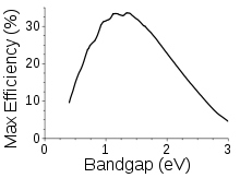
The optical band gap (see below) determines what portion of the solar spectrum a photovoltaic cell absorbs.[6] A semiconductor will not absorb photons of energy less than the band gap; and the energy of the electron-hole pair produced by a photon is equal to the bandgap energy. A luminescent solar converter uses a luminescent medium to downconvert photons with energies above the band gap to photon energies closer to the band gap of the semiconductor comprising the solar cell.[7]
List of band gaps
Below are band gap values for some selected materials. For a comprehensive list of band gaps in semiconductors, see List of semiconductor materials.
| Group | Material | Symbol | Band gap (eV) @ 302K | Reference |
|---|---|---|---|---|
| III-V | Aluminium nitride | AlN | 6.0 | [8] |
| IV | Diamond | C | 5.5 | [9] |
| IV | Silicon | Si | 1.14 | [10] |
| IV | Germanium | Ge | 0.67 | [10] |
| III–V | Gallium nitride | GaN | 3.4 | [10] |
| III–V | Gallium phosphide | GaP | 2.26 | [10] |
| III–V | Gallium arsenide | GaAs | 1.43 | [10] |
| IV–V | Silicon nitride | Si3N4 | 5 | |
| IV–VI | Lead(II) sulfide | PbS | 0.37 | [10] |
| IV–VI | Silicon dioxide | SiO2 | 9 | [11] |
| Copper oxide | Cu2O | 2.1 | [12] |
Optical versus electronic bandgap
In materials with a large exciton binding energy, it is possible for a photon to have just barely enough energy to create an exciton (bound electron–hole pair), but not enough energy to separate the electron and hole (which are electrically attracted to each other). In this situation, there is a distinction between "optical band gap" and "electrical band gap" (or "transport gap"). The optical bandgap is the threshold for photons to be absorbed, while the transport gap is the threshold for creating an electron–hole pair that is not bound together. The optical bandgap is at lower energy than the transport gap.
In almost all inorganic semiconductors, such as silicon, gallium arsenide, etc., there is very little interaction between electrons and holes (very small exciton binding energy), and therefore the optical and electronic bandgap are essentially identical, and the distinction between them is ignored. However, in some systems, including organic semiconductors and single-walled carbon nanotubes, the distinction may be significant.
Band gaps for other quasi-particles
In photonics, band gaps or stop bands are ranges of photon frequencies where, if tunneling effects are neglected, no photons can be transmitted through a material. A material exhibiting this behaviour is known as a photonic crystal. The concept of hyperuniformity[13] has broadened the range of photonic band gap materials, beyond photonic crystals. By applying the technique in supersymmetric quantum mechanics, a new class of optical disordered materials has been suggested,[14] which support band gaps perfectly equivalent to those of crystals or quasicrystals.
Similar physics applies to phonons in a phononic crystal.[15]
Materials
List of electronics topics
- Electronics
- Bandgap voltage reference
- Condensed matter physics
- Direct and indirect bandgaps
- Electrical conduction
- Electron hole
- Field-effect transistor
- Light-emitting diode
- Photodiode
- Photoresistor
- Photovoltaics
- Solar cell
- Solid state physics
- Semiconductor
- Semiconductor devices
- Strongly correlated material
- Valence band
See also
- Wide bandgap semiconductors
- Band bending
- Spectral density
- Pseudogap
- Tauc plot
- Moss–Burstein effect
References
- Babu, V.Suresh (2010). Solid State Devices and Technology, 3rd Edition. Peason.
- Ünlü, Hilmi (September 1992). "A thermodynamic model for determining pressure and temperature effects on the bandgap energies and other properties of some semiconductors". Solid-State Electronics. 35 (9): 1343–1352. Bibcode:1992SSEle..35.1343U. doi:10.1016/0038-1101(92)90170-H.
- Varshni, Y.P. (January 1967). "Temperature dependence of the energy gap in semiconductors". Physica. 34 (1): 149–154. doi:10.1016/0031-8914(67)90062-6.
- “Evident Technologies” Archived 2009-02-06 at the Wayback Machine. Evidenttech.com. Retrieved on 2013-04-03.
- Dean, K J (August 1984). "Waves and Fields in Optoelectronics: Prentice-Hall Series in Solid State Physical Electronics". Physics Bulletin. 35 (8): 339. doi:10.1088/0031-9112/35/8/023.
- Nanoscale Material Design. Nrel.gov. Retrieved on 2013-04-03.
- Nanocrystalline luminescent solar converters, 2004
- Feneberg, Martin; Leute, Robert A. R.; Neuschl, Benjamin; Thonke, Klaus; Bickermann, Matthias (16 August 2010). "High-excitation and high-resolution photoluminescence spectra of bulk AlN". Physical Review B. 82 (7): 075208. Bibcode:2010PhRvB..82g5208F. doi:10.1103/PhysRevB.82.075208.
- Kittel, Charles. Introduction to Solid State Physics, 7th Edition. Wiley.
- Streetman, Ben G.; Sanjay Banerjee (2000). Solid State electronic Devices (5th ed.). New Jersey: Prentice Hall. p. 524. ISBN 0-13-025538-6.
- Vella, E.; Messina, F.; Cannas, M.; Boscaino, R. (2011). "Unraveling exciton dynamics in amorphous silicon dioxide: Interpretation of the optical features from 8 to 11 eV". Physical Review B. 83 (17): 174201. Bibcode:2011PhRvB..83q4201V. doi:10.1103/PhysRevB.83.174201.
- Baumeister, P.W. (1961). "Optical Absorption of Cuprous Oxide". Physical Review. 121 (2): 359. Bibcode:1961PhRv..121..359B. doi:10.1103/PhysRev.121.359.
- Xie, R.; Long, G. G.; Weigand, S. J.; Moss, S. C.; Carvalho, T.; Roorda, S.; Hejna, M.; Torquato, S.; Steinhardt, P. J. (29 July 2013). "Hyperuniformity in amorphous silicon based on the measurement of the infinite-wavelength limit of the structure factor". Proceedings of the National Academy of Sciences. 110 (33): 13250–13254. Bibcode:2013PNAS..11013250X. doi:10.1073/pnas.1220106110. PMC 3746861. PMID 23898166.
- Yu, Sunkyu; Piao, Xianji; Hong, Jiho; Park, Namkyoo (16 September 2015). "Bloch-like waves in random-walk potentials based on supersymmetry". Nature Communications. 6 (1): 8269. arXiv:1501.02591. Bibcode:2015NatCo...6E8269Y. doi:10.1038/ncomms9269. PMC 4595658. PMID 26373616.
- Eichenfield, Matt; Chan, Jasper; Camacho, Ryan M.; Vahala, Kerry J.; Painter, Oskar (2009). "Optomechanical crystals". Nature. 462 (7269): 78–82. arXiv:0906.1236. doi:10.1038/nature08524. ISSN 0028-0836. PMID 19838165.
External links
- Direct Band Gap Energy Calculator
- Moriarty, Philip. "Energy Gap (and what makes glass transparent?)". Sixty Symbols. Brady Haran for the University of Nottingham.