Single-photon avalanche diode
A single-photon avalanche diode (SPAD) is a solid-state photodetector in which a photon-generated carrier (via the internal photoelectric effect) can trigger a short-duration but relatively large avalanche current. This avalanche is created through a mechanism called impact ionization, whereby carriers (electrons and/or holes) are accelerated to high kinetic energies through a large potential gradient (voltage). If the kinetic energy of a carrier is sufficient (as a function of the ionization energy of the bulk material) further carriers are liberated from the atomic lattice. The number of carriers thus increases exponentially from, in some cases, as few as a single carrier. This mechanism was observed and modeled by John Townsend for trace-gas vacuum tubes, becoming known as a Townsend discharge, and later being attributed to solid-state breakdown by K. McAfee. This device is able to detect low-intensity ionizing radiation, including: gamma, X-ray, beta, and alpha-particle radiation along with electromagnetic signals in the UV, Visible and IR (in the optical case this can be down to the single photon level). SPADs are also able to distinguish the arrival times of events (photons) with a timing jitter of a few tens of picoseconds.
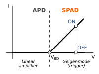
SPADs, like avalanche photodiodes (APDs), exploit the incident radiation triggered avalanche current of a p–n junction when reverse biased. The fundamental difference between SPADs and APDs is that SPADs are specifically designed to operate with a reverse-bias voltage well above the breakdown voltage. This kind of operation is also called Geiger-mode in the literature (as opposed to the linear-mode for the case of an APD). This is in analogy with the Geiger counter.
Since the 1970s, the applications of SPADs have increased significantly. Recent examples of their use include LIDAR, Time of Flight (ToF) 3D Imaging, PET scanning, single-photon experimentation within physics, fluorescence lifetime microscopy and optical communications (particularly quantum key distribution). Notable companies that have commercialized SPAD technology include: ST Microelectronics, Tower Jazz, Phillips and Micro Photon Devices (MPD). The related technologies of solid-state silicon photomultipliers (Si-PMs) and multi-pixel photon counters (MPPCs) have been commercialized and available through companies such as SensL (currently part of ON Semiconductor) and Hamamatsu.
History and technical development
The history and development of SPADs and APDs shares a number of important points with the development of solid-state technologies such as diodes and early p–n junction transistors (particularly war-efforts at Bell Labs). This history can be traced to the late 1890s and early 1900s, however suitable references for the historical development of these devices, can be found for the years 1900 to 1969 [1], along with a number of overview historical [2] and technical reviews [3]. John Townsend in 1901 and 1903 investigated the ionisation of trace gases within vacuum tubes, finding that as the electric potential increased gasious atoms and molecules could become ionised by the kinetic energy of free electrons accelerated though the electric field. The new liberated electrons were then themselves accelerated by the field, producing new ionisations once their kinetic energy has reached sufficient levels. This theory was later instrumental in the development of the thyratron and the Geiger-Mueller Tube. The Townsend Discharge was also instrumental as a base theory for electron multiplication phenomena, (both DC and AC), within both Silicon and Germanium [1].
However, the major advances in early discovery and utilisation of the avalanche gain mechanism were a product of the study of Zener breakdown, related (avalanche) breakdown mechanisms and structural defects in early silicon and germanium transistor and p–n junction devices. These defects were called 'microplasmas' and are critical in the history of APDs and SPADs. Likewise investigation of the light detection properties of p–n junctions is crucial, especially the early 1940s findings by Russel Ohl. Light detection in semiconductors and solids through the internal photoelectric effect is older with Foster Nix [4] pointing to the work of Gudden and Pohl in the 1920s. In the 1950s and 1960s, significant effort was made to reduce the number of Microplasma breakdown and noise sources, with artificial microplasmas being fabricated for study. It became clear that the avalanche mechanism could be useful for signal amplification within the diode itself, as both light and alpha particles were used for the study of these devices and breakdown mechanisms.
In the early 2000s, SPADs have been implemented within CMOS processes. This has radically increased their performance, (dark count rate, jitter, array pixel pitch etc), and has leveraged the analog and digital circuits that can be implemented alongside these devices. Notable circuits include photon counting using fast digital counters, photon timing using both time-to-digital converters (TDCs) and time-to-analog converters (TACs), passive quenching circuits using either NMOS or PMOS transistors in place of poly-silicon resistors, active quenching and reset circuits for high counting rates, and many on-chip digital signal processing blocks. Such devices, now reaching optical fill factors of >70%, with >1024 SPADs, with DCRs < 10Hz and jitter values in the 50ps region are now available with dead times of 1-2ns . Recent devices have leaveraged 3D-IC technologies such as through-silicon-vias (TSVs) to present a high-fill-factor SPAD optimised top CMOS layer (90nm or 65nm node) with a dedicated signal processing and readout CMOS layer (45nm node). Significant advancements in the noise terms for SPADs have been obtained by silicon process modelling tools such as TCAD, where guard rings, junction depths and device structures and shapes can be optimised prior to validation by experimental SPAD structures.
Operating principle
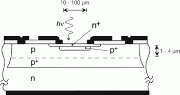
SPADs are semiconductor devices based on a p–n junction reverse-biased at a voltage Va that exceeds breakdown voltage VB of the junction (Figure 1).[5] "At this bias, the electric field is so high [higher than 3×10⁵ V/cm] that a single charge carrier injected into the depletion layer can trigger a self-sustaining avalanche. The current rises swiftly [sub-nanosecond rise-time] to a macroscopic steady level in the milliampere range. If the primary carrier is photo-generated, the leading edge of the avalanche pulse marks [with picosecond time jitter ] the arrival time of the detected photon."[5] The current continues until the avalanche is quenched by lowering the bias voltage VD down to or below VB:[5] the lower electric field is no longer able to accelerate carriers to impact-ionize with lattice atoms, therefore current ceases. In order to be able to detect another photon, the bias voltage must be raised again above breakdown.[5]
"This operation requires a suitable circuit, which has to:
- sense the leading edge of the avalanche current.
- generate a standard output pulse synchronous with the avalanche build-up.
- quench the avalanche by lowering the bias down to the breakdown voltage.
- restore the photodiode to the operative level.
This circuit is usually referred to as a quenching circuit."[5]
Passive quenching
The simplest quenching circuit is commonly called Passive Quenching Circuit and comprises a single resistor in series with the SPAD. This experimental setup has been employed since the early studies on the avalanche breakdown in junctions. The avalanche current self-quenches simply because it develops a voltage drop across a high-value ballast load RL (about 100 kΩ or more). After the quenching of the avalanche current, the SPAD bias VD slowly recovers to Va, and therefore the detector is ready to be ignited again. This circuit mode is therefore called passive quenching passive reset (PQPR), although an active circuit element can be used for reset forming a passive quench active reset (PQAR) circuit mode. A detailed description of the quenching process is reported by Zappa et al.[5]
Active quenching
A more advanced quenching, which was explored from the 1970s onwards, is a scheme called active quenching. In this case a fast discriminator senses the steep onset of the avalanche current across a 50 Ω resistor (or integrated transistor) and provides a digital (CMOS, TTL, ECL, NIM) output pulse, synchronous with the photon arrival time. The circuit then quickly reduces the bias voltage to below breakdown (active quenching), then relatively quickly returns bias to above the breakdown voltage ready to sense the next photon. This mode is called active quench active reset (AQAR), however depending on circuit requirements, active quenching passive reset (AQPR) may be more suitable. AQAR circuits often allow lower dead times, and significantly reduced dead time variation.
Photon counting and timing
The intensity of the signal is obtained by counting (photon counting) the number of output pulses within a measurement time slot, while the time-dependent waveform of the signal is obtained by measuring the time distribution of the output pulses (photon timing). The latter is obtained by means of operating the Single Photon Avalanche Diode (SPAD) detector in time-correlated single photon counting (TCSPC) mode.
Saturation
While the avalanche recovery circuit is quenching the avalanche and restoring bias, the SPAD cannot detect photons. Any photons, (or dark counts or after-pulses), that reach the detector during this brief period are not counted. As the number of photons increases such that the (statistical) time interval between photons gets within a factor of ten or so of the avalanche recovery time, missing counts become statistically significant and the count rate begins to depart from a linear relationship with detected light level. At this point the SPAD begins to saturate. If the light level were to increase further, ultimately to the point where the SPAD immediately avalanches the moment the avalanche recovery circuit restores bias, the count rate reaches a maximum defined purely by the avalanche recovery time in the case of active quenching (hundred million counts per second or more[6]). This can be harmful to the SPAD as it will be experiencing avalanche current nearly continuously. In the passive case, saturation may lead to the count rate decreasing once the maximum is reached. This is called paralysis, whereby a photon arriving as the SPAD is passively recharging, has a lower detection probability, but can extend the dead time. It is worth noting that passive quenching, while simpler to implement in terms of circuitry, incurs a 1/e reduction in maximum counting rates.
Internal noise and afterpulsing
Besides photon-generated carriers, thermally-generated carriers (through generation-recombination processes within the semiconductor) can also fire the avalanche process. Therefore, it is possible to observe output pulses when the SPAD is in complete darkness. The resulting average number of counts per second is called dark count rate and is the key parameter in defining the detector noise. It is worth noting that the reciprocal of the dark count rate defines the mean time that the SPAD remains biased above breakdown before being triggered by an undesired thermal generation. Therefore, in order to work as a single-photon detector, the SPAD must be able to remain biased above breakdown for a sufficiently long time (e.g., a few milliseconds, corresponding to a count rate well under a thousand counts per second, cps).
One other effect that can trigger an avalanche is known as afterpulsing. When an avalanche occurs, the PN junction is flooded with charge carriers and trap levels between the valence and conduction band become occupied to a degree that is much greater than that expected in a thermal-equilibrium distribution of charge carriers. After the SPAD has been quenched, there is some probability that a charge carrier in a trap level receives enough energy to free it from the trap and promote it to the conduction band, which triggers a new avalanche. Thus, depending on the quality of the process and exact layers and implants that were used to fabricate the SPAD, a significant number of extra pulses can be developed from a single originating thermal or photo-generation event. The degree of afterpulsing can be quantified by measuring the autocorrelation of the times of arrival between avalanches when a dark count measurement is set up. Thermal generation produces Poissonian statistics with an impulse function autocorrelation, and afterpulsing produces non-Poissonian statistics.
I-V characteristic
If a SPAD is observed by an analogue curve-tracer, it is possible to observe a bifurcation of the current-voltage characteristics beyond breakdown, during the voltage sweeps applied to the device. When the avalanche is triggered, the SPAD sustains the avalanche current (on-branch), instead when no carrier has been generated (by a photon or a thermal generation), no charge flows through the SPAD (off-branch). If the SPAD is triggered during a sweep above breakdown, a transition from the off-branch to the on-branch can be easily observed (like a "flickering"). Some authors in the literature have denoted this phenomenon as bifurcation.
Fill factor
Arrays of SPADs have been fabricated for some time, however a critical issue is one of diode geometry. As SPADs require a guard ring to prevent premature edge breakdown, the optical fill factor becomes a product of the diode shape and size with relation to the guard rings and inter-diode spacing. The fill factor of a SPAD array is defined as the ratio of the optically active area, where photon counts are detected, to the total area of the array. However in the literature, fill factors vary in terms of if the entire planar device (including readout circuitry and pads) is taken as the total area or if the functional 'array' only is taken. Changes in SPAD size can increase fill factor, however noise may also increase. Likewise topological shapes such as squares and rectangles yield high geometrical fill factors, but lead to increased fields at diode corners and typically higher dark count rates. To compromise, squares with sufficiently rounded edges have been fabricated, i.e. the so-called super-ellipse, Lamé curve, or the Fermat shape. This latter nomenclature is common within the literature, however strictly speaking: "In particular, when a = b = 1 and n is an even integer, then it is a Fermat curve of degree n". Many diodes of the 'Fermat' type are optimized for both high fill factor and minimum noise. As such many will have parameters free of the "a = b = 1 and n is an even integer" restriction.
Comparison with APDs
Both APDs and SPADs are reverse biased semiconductor p–n junctions. However, APDs are biased close to, but not exceeding the breakdown voltage of the semiconductor. This high electric field provides an internal multiplication gain only of the order of few hundreds, since the avalanche process is not diverging (also known as run-away avalanche) as in the case of SPAD avalanche discharges. The resulting avalanche current intensity is linearly related to the optical signal intensity. A SPAD, however, operates with a bias voltage above the breakdown voltage. Because the device is operating in this unstable above-breakdown regime, a single photon (or a single dark-current electron) can set off a significant avalanche of carriers. Practically, this means that in an APD, a single photon produces only tens or few hundreds of electrons, but in a SPAD a single photon triggers a current in the milliampere region (billions of billions of electrons per second) that can be easily "counted".[7]
Therefore, while the APD is a linear amplifier for the input optical signal with limited gain, the SPAD is a trigger device, so the gain concept is meaningless.
See also
References
- 1 2 Fisher, Edward (March 2018). "Principles and Early Historical Development of Silicon Avalanche and Geiger-Mode Photodiodes". Photon Counting (InTechOpen Book) Editors: Nikolay Britun and Anton Nikiforov. 1: 3–37 – via InTechOpen (Public Open Acceess).
- ↑ Renker, D. (2006). "Geiger-mode avalanche photodiodes; history, properties and problems". Nuclear Instruments and Methods in Physics Research A. 567: 48–56.
- ↑ S. Cova, M. Ghioni, A. Lacaita, C. Samori and F. Zappa (1996). "Avalanche photodiodes and quenching circuits for single-photon detection". Applied Optics. 35: 1956–1976 – via OSA Publishing.
- ↑ Nix, Foster (October 1931). "Photoconductivity". Reviews of Modern Physics. 4 (4): 723–766.
- 1 2 3 4 5 6 F. Zappa, S. Cova; M. Ghioni; A. Lacaita; C. Samori (1996-04-20). "Avalanche photodiodes and quenching circuits for single-photon detection" (PDF). Applied Optics. 35 (12): 1956–1976. doi:10.1364/AO.35.001956. PMID 21085320.
- ↑ Eisele, A.; Henderson, R.; Schmidtke, B.; Funk, T.; Grant, L.; Richardson, J.; Freude, W.: 185 MHz count rate, 139 dB dynamic range single-photon avalanche diode with active quenching circuit in 130 nm CMOS technology Intern. Image Sensor Workshop (IISW'11), Hokkaido, Japan; Paper R43; June 2011
- ↑ Fishburn, Matthew (2012). Fundamentals of CMOS Single-Photon Avalanche Diodes. Delft, the Netherlands: Delft University of Technology. pp. 4–5. ISBN 978-94-91030-29-1. Retrieved October 10, 2012.