Intel 8080
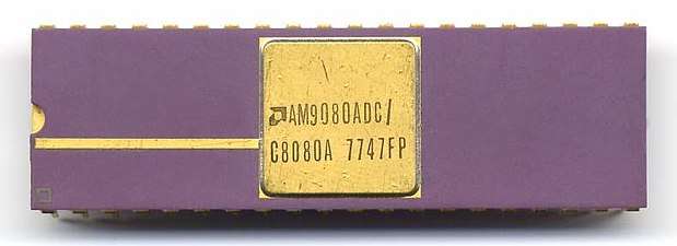
 An Intel C8080A processor | |
| Produced | April 1974 |
|---|---|
| Common manufacturer(s) | |
| Max. CPU clock rate | 2 MHz to 3.125 MHz |
| Min. feature size | 6 µm |
| Instruction set | 8080 |
| Predecessor | Intel 8008 |
| Successor |
Intel 8085 Intel 8086 Intel 8088 |
| Package(s) |
|
The Intel 8080 ("eighty-eighty") was the second 8-bit microprocessor designed and manufactured by Intel and was released in April 1974.[1] It is an extended and enhanced variant of the earlier 8008 design, although without binary compatibility. The initial specified clock frequency limit was 2 MHz, and with common instructions using 4, 5, 7, 10, or 11 cycles this meant that it operated at a typical speed of a few hundred thousand instructions per second. A faster variant 8080A-1 became available later with clock frequency limit up to 3.125 MHz.
The 8080 requires two support chips to function in most applications, the i8224 clock generator/driver and the i8228 bus controller, and it is implemented in NMOS using non-saturated enhancement mode transistors as loads [2][3] therefore demanding a +12 V and a −5 V voltage in addition to the main TTL-compatible +5 V.
Although earlier microprocessors were used for calculators, cash registers, computer terminals, industrial robots,[4] and other applications, the 8080 became one of the first really widespread microprocessors. Several factors contributed to its popularity: its 40-pin package made it easier to interface than the 18-pin 8008, and also made its data bus more efficient; its NMOS implementation gave it faster transistors than those of the PMOS 8008, while also simplifying interfacing by making it TTL-compatible; a wider variety of support chips was available; its instruction set was enhanced over the 8008;[5] and its full 16-bit address bus (versus the 14-bit one of the 8008) enabled it to access 64 KB of memory, four times more than the 8008's range of 16 KB. It became the engine of the Altair 8800, and subsequent S-100 bus personal computers, until it was replaced by the Z80 in this role, and was the original target CPU for CP/M operating systems developed by Gary Kildall.
The 8080 was successful enough that compatibility at the assembly language level became a design requirement for the 8086 when design for it was started in 1976. This also means that the 8080 directly influenced the ubiquitous 32-bit and 64-bit x86 architectures of today.
Description
Programming model
| 15 | 14 | 13 | 12 | 11 | 10 | 09 | 08 | 07 | 06 | 05 | 04 | 03 | 02 | 01 | 00 | (bit position) |
| Main registers | ||||||||||||||||
| A | Flags | Program Status Word | ||||||||||||||
| B | C | B | ||||||||||||||
| D | E | D | ||||||||||||||
| H | L | H (indirect address) | ||||||||||||||
| Index registers | ||||||||||||||||
| SP | Stack Pointer | |||||||||||||||
| Program counter | ||||||||||||||||
| PC | Program Counter | |||||||||||||||
| Status register | ||||||||||||||||
| S | Z | - | AC | - | P | - | C | Flags | ||||||||
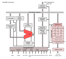
The Intel 8080 is the successor to the 8008. It uses the same basic instruction set and register model as the 8008 (developed by Computer Terminal Corporation), even though it is not source-code compatible nor binary-compatible with its predecessor. Every instruction in the 8008 has an equivalent instruction in the 8080 (even though the actual opcodes differ between the two CPUs). The 8080 also adds a few 16-bit operations in its instruction set as well. Whereas the 8008 required the use of the HL register pair to indirectly access its 14-bit memory space, the 8080 added addressing modes to allow direct access to its full 16-bit memory space. In addition, the internal 7-level push-down call stack of the 8008 was replaced by a dedicated 16-bit stack-pointer (SP) register. The 8080's large 40-pin DIP packaging permits it to provide a 16-bit address bus and an 8-bit data bus, allowing easy access to 64 KB of memory.
Registers
The processor has seven 8-bit registers (A, B, C, D, E, H, and L), where A is the primary 8-bit accumulator, and the other six registers can be used as either individual 8-bit registers or as three 16-bit register pairs (BC, DE, and HL, referred to as B, D and H in Intel documents) depending on the particular instruction. Some instructions also enable the HL register pair to be used as a (limited) 16-bit accumulator, and a pseudo-register M can be used almost anywhere that any other register can be used, referring to the memory address pointed to by the HL pair. It also has a 16-bit stack pointer to memory (replacing the 8008's internal stack), and a 16-bit program counter.
Flags
The processor maintains internal flag bits (a status register), which indicate the results of arithmetic and logical instructions. The flags are:
- Sign (S), set if the result is negative.
- Zero (Z), set if the result is zero.
- Parity (P), set if the number of 1 bits in the result is even.
- Carry (C), set if the last addition operation resulted in a carry or if the last subtraction operation required a borrow
- Auxiliary carry (AC or H), used for binary-coded decimal arithmetic (BCD).
The carry bit can be set or complemented by specific instructions. Conditional-branch instructions test the various flag status bits. The flags can be copied as a group to the accumulator. The A accumulator and the flags together are called the PSW register, or program status word.
Commands/instructions
As with many other 8-bit processors, all instructions are encoded in a single byte (including register numbers, but excluding immediate data), for simplicity. Some of them are followed by one or two bytes of data, which can be an immediate operand, a memory address, or a port number. Like larger processors, it has automatic CALL and RET instructions for multi-level procedure calls and returns (which can even be conditionally executed, like jumps) and instructions to save and restore any 16-bit register pair on the machine stack. There are also eight one-byte call instructions (RST
) for subroutines located at the fixed addresses 00h, 08h, 10h, ..., 38h. These were intended to be supplied by external hardware in order to invoke a corresponding interrupt service routine, but were also often employed as fast system calls. The most sophisticated command is XTHL
, which is used for exchanging the register pair HL with the value stored at the address indicated by the stack pointer.
8-bit instructions
Most 8-bit operations can only be performed on the 8-bit accumulator (the A register). For 8-bit operations with two operands, the other operand can be either an immediate value, another 8-bit register, or a memory byte addressed by the 16-bit register pair HL. Direct copying is supported between any two 8-bit registers and between any 8-bit register and an HL-addressed memory byte. Due to the regular encoding of the MOV
instruction (using a quarter of available opcode space), there are redundant codes to copy a register into itself (MOV B,B
, for instance), which were of little use, except for delays. However, what would have been a copy from the HL-addressed cell into itself (i.e., MOV M,M
) is instead used to encode the halt (HLT
) instruction, halting execution until an external reset or interrupt occurs.
16-bit operations
Although the 8080 is generally an 8-bit processor, it also has limited abilities to perform 16-bit operations: Any of the three 16-bit register pairs (BC, DE, or HL, referred to as B, D, H in Intel documents) or SP can be loaded with an immediate 16-bit value (using LXI
), incremented or decremented (using INX
and DCX
), or added to HL (using DAD
). The XCHG
[6] instruction exchanges the values of the HL and DE register pairs. By adding HL to itself, it is possible to achieve the same result as a 16-bit arithmetical left shift with one instruction. The only 16-bit instructions that affect any flag are DAD H/D/B
, which set the CY (carry) flag in order to allow for programmed 24-bit or 32-bit arithmetic (or larger), needed to implement floating-point arithmetics, for instance.
Input/output scheme
Input output port space
The 8080 supports up to 256[7] input/output (I/O) ports, accessed via dedicated I/O instructions taking port addresses as operands. This I/O mapping scheme was regarded as an advantage, as it freed up the processor's limited address space. Many CPU architectures instead use so-called memory-mapped I/O, in which a common address space is used for both RAM and peripheral chips. This removes the need for dedicated I/O instructions, although a drawback in such designs may be that special hardware must be used to insert wait states, as peripherals are often slower than memory. However, in some simple 8080 computers, I/O was indeed addressed as if they were memory cells, "memory-mapped", leaving the I/O commands unused. I/O addressing could also sometimes employ the fact that the processor would output the same 8-bit port address to both the lower and the higher address byte (i.e. IN 05h
would put the address 0505h on the 16-bit address bus). Similar I/O-port schemes were used in the backward-compatible Zilog Z80 and Intel 8085, as well as the closely related x86 families of microprocessors.
Separate stack space
One of the bits in the processor state word (see below) indicates that the processor is accessing data from the stack. Using this signal, it is possible to implement a separate stack memory space. However, this feature was seldom used.
The internal state word
For more advanced systems, during one phase of its working loop, the processor set its "internal state byte" on the data bus. This byte contains flags that determine whether the memory or I/O port is accessed and whether it is necessary to handle an interrupt.
The interrupt system state (enabled or disabled) is also output on a separate pin. For simple systems, where the interrupts are not used, it is possible to find cases where this pin is used as an additional single-bit output port (the popular Radio-86RK computer made in the Soviet Union, for instance).
Example code
The following 8080/8085 assembler source code is for a subroutine named memcpy that copies a block of data bytes of a given size from one location to another. The data block is copied one byte at a time, and the data movement and looping logic utilizes 16-bit operations.
1000 1000 1000 78 1001 B1 1002 C8 1003 1A 1004 77 1005 13 1006 23 1007 0B 1008 78 1009 B1 100A C2 03 10 100D C9 |
; memcpy --
; Copy a block of memory from one location to another.
;
; Entry registers
;       BC - Number of bytes to copy
;       DE - Address of source data block
;       HL - Address of target data block
;
; Return registers
;       BC - Zero

            org     1000h       ;Origin at 1000h
memcpy      public
            mov     a,b         ;Test BC,
            ora     c           ;If BC = 0,
            rz                  ;Return
loop:       ldax    d           ;Load A from (DE)
            mov     m,a         ;Store A into (HL)
            inx     d           ;Increment DE
            inx     h           ;Increment HL
            dcx     b           ;Decrement BC (does not affect Flags)
            mov     a,b         ;Test for done
            ora     c           ;B | C = 0 and done
            jnz     loop        ;Repeat loop until BC = 0
            ret
|
Pin usage
The address bus has its own 16 pins, and the data bus has 8 pins that are usable without any multiplexing. Using the two additional pins (read and write signals), it is possible to assemble simple microprocessor devices very easily. Only the separate IO space, interrupts and DMA require additional chips to decode the processor pin signals. However, the processor load capacity is limited, and even simple computers frequently contained bus amplifiers.
The processor requires three power sources (−5, +5 and +12 V) and two non-overlapping high-amplitude synchronization signals. However, at least the late Soviet version КР580ВМ80А was able to work with a single +5 V power source, the +12 V pin being connected to +5 V and the −5 V pin to ground. The processor consumes about 1.3 W of power.
The pin-out table, from the chip's accompanying documentation, describes the pins as follows:
| Pin number | Signal | Type | Comment |
|---|---|---|---|
| 1 | A10 | Output | Address bus 10 |
| 2 | GND | — | Ground |
| 3 | D4 | Bidirectional | Bidirectional data bus. The processor also transiently sets here the "processor state", providing information about what the processor is currently doing:
|
| 4 | D5 | ||
| 5 | D6 | ||
| 6 | D7 | ||
| 7 | D3 | ||
| 8 | D2 | ||
| 9 | D1 | ||
| 10 | D0 | ||
| 11 | −5 V | — | The −5 V power supply. This must be the first power source connected and the last disconnected, otherwise the processor will be damaged. |
| 12 | RESET | Input | Reset. The signal forces execution of commands located at address 0000. The content of other processor registers is not modified. This is an inverting input (the active level being logical 0) |
| 13 | HOLD | Input | Direct memory access request. The processor is requested to switch the data and address bus to the high impedance ("disconnected") state. |
| 14 | INT | Input | Interrupt request |
| 15 | φ2 | Input | The second phase of the clock generator signal |
| 16 | INTE | Output | The processor has two commands for setting 0 or 1 level on this pin. The pin normally is supposed to be used for interrupt control. However, in simple computers it was sometimes used as a single bit output port for various purposes. |
| 17 | DBIN | Output | Read (the processor reads from memory or input port) |
| 18 | WR | Output | Write (the processor writes to memory or output port). This is an inverted output, the active level being logical zero. |
| 19 | SYNC | Output | Active level indicates that the processor has put the "state word" on the data bus. The various bits of this state word provide additional information for supporting the separate address and memory spaces, interrupts, and direct memory access. This signal is required to pass through additional logic before it can be used to write the processor state word from the data bus into some external register, e.g. 8238-System Controller and Bus Driver. |
| 20 | +5 V | — | The + 5 V power supply |
| 21 | HLDA | Output | Direct memory access confirmation. The processor switches data and address pins into the high impedance state, allowing another device to manipulate the bus |
| 22 | φ1 | Input | The first phase of the clock generator signal |
| 23 | READY | Input | Wait. With this signal it is possible to suspend the processor's work. It is also used to support the hardware-based step-by step debugging mode. |
| 24 | WAIT | Output | Wait (indicates that the processor is in the waiting state) |
| 25 | A0 | Output | Address bus |
| 26 | A1 | ||
| 27 | A2 | ||
| 28 | 12 V | — | The +12 V power supply. This must be the last connected and first disconnected power source. |
| 29 | A3 | Output | The address bus; can switch into high impedance state on demand |
| 30 | A4 | ||
| 31 | A5 | ||
| 32 | A6 | ||
| 33 | A7 | ||
| 34 | A8 | ||
| 35 | A9 | ||
| 36 | A15 | ||
| 37 | A12 | ||
| 38 | A13 | ||
| 39 | A14 | ||
| 40 | A11 |
Support chips
A key factor in the success of the 8080 was the broad range of support chips available, providing serial communications, counter/timing, input/output, direct memory access, and programmable interrupt control amongst other functions:
- 8238 – System controller and bus driver
- 8251 – Communication controller
- 8253 – Programmable interval timer
- 8255 – Programmable peripheral interface
- 8257 – DMA controller
- 8259 – Programmable interrupt controller
Physical implementation
The 8080 integrated circuit uses non-saturated enhancement-load nMOS gates, demanding extra voltages (for the load-gate bias). It was manufactured in a silicon gate process using a minimal feature size of 6 µm. A single layer of metal is used to interconnect the approximately 6,000 transistors[8] in the design, but the higher resistance polysilicon layer, which required higher voltage for some interconnects, is implemented with transistor gates. The die size was approximately 20 mm2.
The industrial impact
Applications and successors
The 8080 is used in many early microcomputers, such as the MITS Altair 8800 Computer, Processor Technology SOL-20 Terminal Computer and IMSAI 8080 Microcomputer, forming the basis for machines running the CP/M operating system (the later, almost fully compatible and more capable, Zilog Z80 processor would capitalize on this, with Z80 & CP/M becoming the dominant CPU & OS combination of the period circa 1976 to 1983 much as did the x86 & MS-DOS for the PC a decade later).
Even in 1979 after introduction of the Z80 and 8085 processors, five manufacturers of the 8080 were selling an estimated 500,000 units per month at a price around $3 to $4 per unit.[9]
The first single-board microcomputers, such as MYCRO-1 and the dyna-micro were based on the Intel 8080. One of the early uses of the 8080 was made in the late 1970s by Cubic-Western Data of San Diego, CA in its Automated Fare Collection Systems custom designed for mass transit systems around the world. An early industrial use of the 8080 is as the "brain" of the DatagraphiX Auto-COM (Computer Output Microfiche) line of products which takes large amounts of user data from reel-to-reel tape and images it onto microfiche. The Auto-COM instruments also include an entire automated film cutting, processing, washing, and drying sub-system – quite a feat, both then and in the 21st century, to all be accomplished successfully with only an 8-bit microprocessor running at a clock speed of less than 1 MHz with a 64 KB memory limit. In addition, several early arcade video games were built around the 8080 microprocessor, including Space Invaders, one of the most popular arcade games ever made.
Shortly after the launch of the 8080, the Motorola 6800 competing design was introduced, and after that, the MOS Technology 6502 derivative of the 6800.
Zilog introduced the Z80, which has a compatible machine-language instruction set and initially used the same assembly language as the 8080, but for legal reasons, Zilog developed a syntactically-different (but code compatible) alternative assembly language for the Z80. At Intel, the 8080 was followed by the compatible and electrically more elegant 8085.
Later Intel issued the assembly-language compatible (but not binary-compatible) 16-bit 8086 and then the 8/16-bit 8088, which was selected by IBM for its new PC to be launched in 1981. Later NEC made the NEC V20 (an 8088 clone with Intel 80186 instruction set compatibility) which also supports an 8080 emulation mode. This is also supported by NEC's V30 (a similarly enhanced 8086 clone). Thus, the 8080, via its ISA, made a lasting impact on computer history.
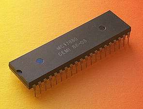
A number of processors compatible with the Intel 8080A were manufactured in the Eastern Bloc: the KR580VM80A (initially marked as KP580ИK80) in the Soviet Union, the MCY7880[10] made by Unitra CEMI in Poland, the MHB8080A[11] made by TESLA in Czechoslovakia, the 8080APC[11] made by Tungsram / MEV in Hungary, and the MMN8080[11] made by Microelectronica Bucharest in Romania.
As of 2017, the 8080 is still in production at Lansdale Semiconductors.[12]
- Intel 8080 second sources
 CEMI MCY7880 (Poland)
 Kvazar Kiev K580IK80 (Soviet Union)
 Mitsubishi Electric M5L8080
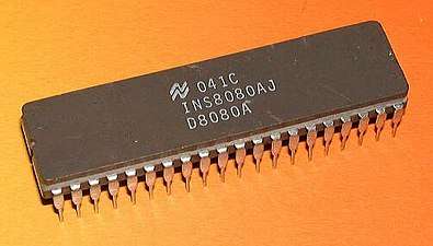 National Semiconductor INS8080
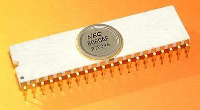 NEC 8080
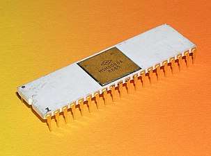 OKI MSM8080
 Siemens SAB8080
 Signetics MP8080
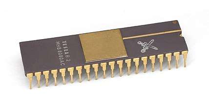 Tesla (Czechoslovak company) MHB8080
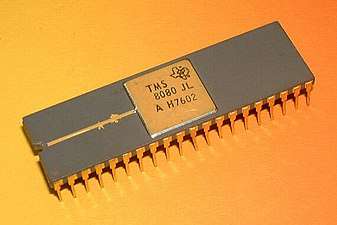 Texas Instruments TMS8080
Industry change
The 8080 also changed how computers were created. When the 8080 was introduced, computer systems were usually created by computer manufacturers such as Digital Equipment Corporation, Hewlett Packard, or IBM. A manufacturer would produce the entire computer, including processor, terminals, and system software such as compilers and operating system. The 8080 was actually designed for just about any application except a complete computer system. Hewlett Packard developed the HP 2640 series of smart terminals around the 8080. The HP 2647 is a terminal which runs BASIC on the 8080. Microsoft would market as its founding product the first popular programming language for the 8080, and would later acquire DOS for the IBM PC.
The 8080 and 8085 gave rise to the 8086, which was designed as a source compatible (although not binary compatible) extension of the 8085. This design, in turn, later spawned the x86 family of chips, the basis for most CPUs in use today. Many of the 8080's core machine instructions and concepts, for example, registers named A, B, C and D, as well as many of the flags used to control conditional jumps, are still in use in the widespread x86 platform. 8080 Assembler code can still be directly translated into x86 instructions; all of its core elements are still present.
PCs based upon the 8086 design and its successors evolved into workstations and servers of 16, 32 and 64 bits, with advanced memory protection, segmentation, and multiprocessing features, blurring the difference between small and large computers (the 80286 and 80386's protected mode were important in doing so). The size of chips has grown so that the size and power of large x86 chips is not much different from high end architecture chips, and a common strategy to produce a very large computer is to network many x86 processors.
History
Federico Faggin, the originator of the 8080 architecture in early 1972, proposed it to Intel's management and pushed for its implementation. He finally got the permission to develop it six months later. Faggin hired Masatoshi Shima from Japan, who did the detailed design under his direction, using the design methodology for random logic with silicon gate that Faggin had created for the 4000 family. Stanley Mazor contributed a couple of instructions to the instruction set.
Patent
- US patent 4010449, Federico Faggin, Masatoshi Shima, Stanley Mazor, "MOS computer employing a plurality of separate chips", issued March 1, 1977
Cultural impact
- Asteroid 8080 Intel is named as a pun and praise on the name of Intel 8080.[13]
- Microsoft's published phone number, 425-882-8080, was chosen because so much early work was on this chip.
- Many of Intel's main phone numbers also take a similar form: xxx-xxx-8080
See also
References
- ↑ Intel (April 15, 1974). "From CPU to software, the 8080 Microcomputer is here". Electronic News. New York: Fairchild Publications. pp. 44–45. Electronic News was a weekly trade newspaper. The same advertisement appeared in the May 2, 1974 issue of Electronics magazine.
- ↑ similar to pull-up resistors
- ↑ Tohya, Hirokazu (2013). Switching Mode Circuit Analysis and Design: Innovative Methodology by Novel Solitary Electromagnetic Wave Theory. Bentham Science Publishers. p. 4. ISBN 9781608054497.
- ↑ The 8008 (1972) was used for interpolation and control in ASEA's (now ABB) first line of general industrial robots, introduced October 1973.
- ↑ The enhancements were largely based on customer feedback and Federico Faggin and others listening to minicomputer-oriented professionals about certain problems and lack of features in the 8008 architecture. (Source: 8008 and 8080 oral histories.)
- ↑ 8080 instruction encoding. ClassicCMP.org. Retrieved on October 23, 2011.
- ↑ Note: Some Intel datasheets from the 1970s advertise 512 I/O ports, because they count input and output ports separately.
- ↑ Reichel-Orbital museum – CPU Collection. Museum.reichel-orbital.de. Retrieved on October 23, 2011.
- ↑ Sol Libes (November 1979). "BYTE News". BYTE Magazine. 11. 4. p. 82. ISSN 0360-5280.
- ↑ MCY7880—a Polish-made clone of 8080. CPU World. Retrieved on October 23, 2011.
- 1 2 3 Soviet chips and their western analogs. CPU-world. Retrieved on October 23, 2011.
- ↑ "Intel - Microprocessor 8080A Family & 828X Series". Lansdale Semiconductor Inc. Retrieved 20 June 2017.
- ↑ CFA-harvard.edu. CFA-harvard.edu. Retrieved on October 23, 2011.
External links
- Intel and other manufacturers' 8080 CPU images and descriptions at cpu-collection.de
- Scan of the Intel 8080 data book at DataSheetArchive.com
- Microcomputer Design, Second Edition, 1976
- 8080 Emulator written in JavaScript
- Intel 8080/KR580VM80A emulator in JavaScript
- Intel 8080 Microcomputer Systems User's Manual (September 1975, 262 pages)
- Intel 8080 Microcomputer Systems User's Manual (September 1975, 234 pages)
This article is based on material taken from the Free On-line Dictionary of Computing prior to 1 November 2008 and incorporated under the "relicensing" terms of the GFDL, version 1.3 or later.
| Authority control |
|---|