Intel 4004
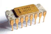 White ceramic Intel C4004 microprocessor with grey traces | |
| Produced | From late 1971 to 1981 |
|---|---|
| Common manufacturer(s) |
|
| Max. CPU clock rate | 740 kHz |
| Min. feature size | 10 µm |
| Instruction set | 4-bit BCD-oriented |
| Transistors | 2300[1] |
| Data width | 4 |
| Address width | 12 (multiplexed) |
| Successor | Intel 4040 |
| Application | Busicom calculator, arithmetic manipulation |
| Package(s) |
|
The Intel 4004 is a 4-bit central processing unit (CPU) released by Intel Corporation in 1971. It was the first commercially available microprocessor by Intel,[2] and the first in a long line of Intel CPUs.
The chip design started in April 1970, when Federico Faggin joined Intel, and was completed under his leadership in January 1971. The first commercial sale of the fully operational 4004 occurred in March 1971 to Busicom Corp. of Japan for which it was originally designed and built as a custom chip.[3] In mid-November of the same year, with the prophetic ad "Announcing a new era in integrated electronics", the 4004 was made commercially available to the general market. The 4004 was the first commercially available monolithic CPU, fully integrated in one small chip. Such a feat of integration was made possible by the use of the then-new silicon gate technology for integrated circuits, originally developed by Faggin (with Tom Klein) at Fairchild Semiconductor in 1968, which allowed twice the number of random-logic transistors and an increase in speed by a factor of five compared to the incumbent MOS aluminum gate technology.[4] Faggin also invented the bootstrap load with silicon gate and the “buried contact”, improving speed and circuit density compared with aluminum gate.[5][6][7][8][9]
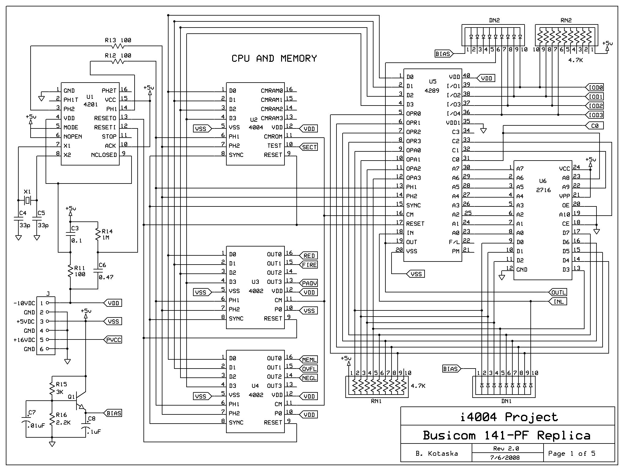
The 4004 microprocessor, the 4001 ROM, 4002 RAM, and 4003 Shift Register constituted the 4 chips in the Intel MCS-4 chip-set. With these components, small computers with varying amounts of memory and I/O facilities can be built.
Contemporaneous CPU chips
Three other CPU chip designs were produced at about the same time: the Four-Phase Systems AL1, done in 1969; the MP944, completed in 1970 and used in the F-14 Tomcat fighter jet; and the Texas Instruments TMS-1000 chip, announced in September 17, 1971. Both the AL1 and the MP944 use several chips for the implementation of the CPU function. The TMS0100 chip was presented as a “calculator on a chip” with the original designation TMS1802NC.[10] This chip contains a very primitive CPU and can only be used to implement various simple 4-function calculators. It is the precursor of the TMS1000, introduced in 1974, which is considered the first microcontroller i.e., a computer on a chip containing not only the CPU, but also ROM, RAM, and I/O functions.[11] The MCS-4 family of 4 chips developed by Intel, of which the 4004 is the CPU or microprocessor, was far more versatile and powerful than the single chip TMS1000, allowing the creation of a variety of small computers for various applications.
Zilog, the first company entirely dedicated to microprocessors and microcontrollers, was started by F. Faggin and Ralph Ungermann, at the end of 1974. These devices formed the basis for later models of microcontrollers.
History and production
The first public mention of 4004 was an advertisement in the November 15, 1971, edition of Electronic News.[13] The first delivery was to Busicom for their engineering prototype calculator in March 1971,[14][9] followed by their 141-PF prototype calculator commercially available in the market in July 1971.[15] Packaged in a 16-pin ceramic dual in-line package, the 4004 was the first commercially available computer processor designed and manufactured by chip maker Intel, which had previously made semiconductor memory chips. The chief designers of the chip were Federico Faggin, the leader of the project after the architectural definition was finalized with Busicom, who created the design methodology and the silicon-based chip design; Ted Hoff who formulated the architecture,[16][17] both of Intel, and Masatoshi Shima of Busicom who assisted in the development.
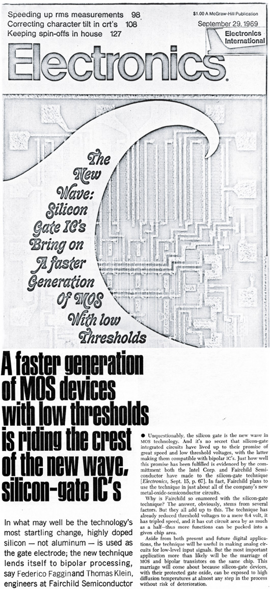
Faggin, the sole chip designer among the engineers on the MCS-4 project, was the only one with experience in metal-oxide semiconductor (MOS) random logic and circuit design. He also had the crucial knowledge of the new silicon gate process technology with self-aligned gates, which he had created at Fairchild in 1968. At Fairchild in 1968, Faggin also designed and manufactured the world's first commercial IC using SGT, the Fairchild 3708 [18] that was featured on the cover of Electronics (Sept. 29, 1969).[19] As soon as he joined the Intel MOS Department he created a new random logic design methodology based on silicon gate,[15] and contributed many technology and circuit design inventions that enabled their single chip microprocessor to become a reality. His methodology set the design style for all the early Intel microprocessors and later for the Zilog Z80. He also led the MCS-4 project and was responsible for its successful outcome (1970–1971). Marcian "Ted" Hoff, head of the Application Research Department, contributed the architectural proposal for Busicom working with Stanley Mazor in 1969, then he moved on to other projects. When asked where he got the ideas for the architecture of the first microprocessor, Hoff related that Plessey, "a British tractor company",[20] had donated a minicomputer to Stanford, and he had "played with it some" while he was there. Shima designed the Busicom calculator firmware and assisted Faggin during the first six months of the implementation. The manager of Intel's MOS Design Department was Leslie L. Vadász.[21] At the time of the MCS-4 development, Vadasz's attention was completely focused on the mainstream business of semiconductor memories and he left the leadership and the management of the MCS-4 project to Faggin.
Busicom had designed their own special-purpose LSI chipset for use in their Busicom 141-PF calculator with integrated printer. They based their design on the architecture of the Olivetti Programma 101, the world’s first tabletop programmable calculator, which Olivetti introduced in 1965. Busicom commissioned Intel to develop their for production. Like the Olivetti Programma 101, the Busicom design used serial read-write memory. The Busicom memory was based on MOS shift registers rather than the costly Olivetti memory based on magnetostriction wire.
Intel determined the Busicom design was too complex, since serial memories required more components, and would use 40 pins, a packaging standard different from Intel’s own 16-pin standard. Intel proposed to develop a new design which could be produced with standard 16-pin DIP packaging, and would have a reduced instruction set.[22] The memory simplification would come from using Intel’s newly developed dynamic RAM memory. This new design was the 4004 chip, which is one of a set of 4 chips, along with ROM, DRAM, and serial-to-parallel shift register chips. The 4004 was subsequently designed by Federico Faggin [23] using silicon gate technology and built of approximately 2,300 transistors[1] and was followed the next year by the first ever 8-bit microprocessor, the 3,500 transistor 8008 (and the 4040, a revised and improved 4004). It was not until the development of the 40-pin 8080 in 1974, a project conceived and directed by Faggin [24] that the address and data buses would be separated, giving faster and simpler access to memory.
The 4004 employs a 10 µm process silicon-gate enhancement load pMOS technology on a 12 mm² die[25] and can execute approximately 92,000 instructions per second; a single instruction cycle is 10.8 microseconds.[26] The original clock rate design goal was 1 MHz, the same as the IBM 1620 Model I.
The Intel 4004 was designed by physically cutting sheets of Rubylith into thin strips to lay out the circuits to be printed, a process made obsolete by current computer graphic design capabilities.[27]
For the purpose of testing the produced chips, Faggin developed a tester for silicon wafers of MCS-4 family that was itself driven by 4004 chip. The tester also served as a proof for the management that Intel 4004 microprocessor could be used not only in calculator-like products, but also for control applications.[28]
Name and variants
When Faggin designed the MCS-4 family, he also christened the chips with distinct names: 4001, 4002, 4003, and 4004, breaking away from the numbering scheme used by Intel at that time which would have required the names 1302, 1105, 1507, and 1202 respectively. Had he followed Intel's number sequence, the idea that the chips were part of a family of components intended to work seamlessly together would have been lost.[29] Intel's early numbering scheme for integrated circuits used a four-digit number for each component. The first digit indicated the process technology used, the second digit indicated the generic function, and the last two digits of the number were used to indicate the sequential number in the development of the component. The 8008 microprocessor was originally called 1201, per Intel’s naming conventions. Before its market introduction, the 1201 was renamed 8008, following the new naming convention started with the 4001/2/3/4.
Tadashi Sasaki attributes the basic invention to break the calculator into four parts with ROM (4001), RAM (4002), shift registers (4003) and CPU (4004) to an unnamed woman from the Nara Women's College present at a brainstorming meeting that was held in Japan prior to his first meeting with Robert Noyce from Intel, leading up to the Busicom deal.[30]
The 4004 is part of the MCS-4 family of LSI chips that can be used to build digital computers with varying amounts of memory. The other members of the MCS-4 family are memories and input/output circuits, which are necessary to implement a complete computer. The 4001 is a ROM (read-only memory) with four lines of output; the 4002 is a RAM (random access memory) with four lines of input/output. The 4003 is a static shift register to be used for expanding the I/O lines; e.g., for keyboard scanning or controlling a printer.
The 4004 includes functions for direct low-level control of memory chip selection and I/O, which are not normally handled by the microprocessor; however, its functionality is limited in that it cannot execute code from RAM and is limited to whatever instructions are provided in ROM (or an independently-loaded RAM working as ROM - in either case, the processor is itself unable to write or transfer data into an executable memory space). The RAM and ROM parts were also unusual in their integration of output (and, in the ROMs, input) ports that significantly reduced the minimum part count in an MCS-4 system, but required inclusion of a certain amount of processor-like logic on the chips themselves to accept, decode and execute relatively high-level data transfer instructions.
The standard arrangement for a 4004 system is anything up to 16 x 4001 ROM chips (in a single bank) and 16 x 4002 RAM chips (in four banks of four), which together provide the 4KB program storage, 1024 + 256 nibbles of data/status storage, plus 64 output and 64 input/output external data/control lines (which can themselves be used to operate, e.g. a 4003). Intel's MCS-4 documentation, however, claims that upto 48 ROM and RAM chips (providing upto 192 external control lines) "in any combination" can be connected to the 4004 "with simple gating hardware", but declines to give any further detail or examples of how this would actually be achieved.
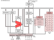
Technical specifications
.jpg)
| Intel 4004 registers | ||||||||||||||||||||||||||||||||||||||||||||||||||||||||||||||||||||||||||||||||||||||||||||||||||||||||||||||||||||||||||||||||||||||||||||||||||||||||||||||||||||||||||||||||||||||||||||||||||||||||||||||||||||||||||||||||||||||||||||||||||||||||||||||||||||
| ||||||||||||||||||||||||||||||||||||||||||||||||||||||||||||||||||||||||||||||||||||||||||||||||||||||||||||||||||||||||||||||||||||||||||||||||||||||||||||||||||||||||||||||||||||||||||||||||||||||||||||||||||||||||||||||||||||||||||||||||||||||||||||||||||||
- Maximum clock rate is 740 kHz. The 4004 had this maximum clock rating upon its initial 1971 release[Note 1]
- Instruction cycle time: minimum 10.8 µs[31] (8 clock cycles / machine cycle)
- Instruction execution time 1 or 2 machine cycles (10.8 or 21.6 µs), 46250 to 92500 instructions per second.
- Adding two 8-digit numbers (32 bits each, assuming 4-bit BCD digits) takes a claimed 850 µs, or approximately 79 machine cycles (632 clock ticks), for an average of just under 10 cycles (80 ticks) per digit pair and an operating speed of 1176 x 8-digit additions per second[Note 2]
- Separate program and data storage. Contrary to Harvard architecture designs, however, which use separate buses, the 4004, with its need to keep pin count down, uses a single multiplexed 4-bit bus for transferring:
- 12-bit addresses
- 8-bit instructions
- 4-bit data words
- Able to directly address 5120 bits (equivalent to 640 bytes) of RAM, stored as 1280 4-bit "characters" and organised into groups representing 1024 "data" and 256 "status" characters (512 and 128 bytes).[Note 3]
- Able to directly address 32768 bits of ROM, equivalent to and arranged as 4096 8-bit words (i.e. bytes).[Note 4]
- Instruction set contained 46 instructions (of which 41 were 8 bits wide and 5 were 16 bits wide)
- Register set contains 16 registers of 4 bits each
- Internal subroutine stack, 3 levels deep.
Logic levels
| Symbol | Min | Max | Unit |
|---|---|---|---|
| VSS-DD | +15-5% | +15+5% | V |
| VIL | VDD | VSS−5.5 | V |
| VIH | VSS−1.5 | VSS+0.3 | V |
| VOL | VSS−12 | VSS−6.5 | V |
| VOH | VSS−0.5 | VSS | V |
Support chips
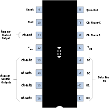
- 4001: 256-byte ROM (256 8-bit program instructions), and one built-in 4-bit I/O port. A 4001 ROM+I/O chip cannot be used in a system along with a 4008/4009 pair.[32]
- 4002: 40-byte RAM (80 4-bit data words), and one built-in 4-bit output port; the RAM portion of the chip is organized into four "registers" of 20 4-bit words:
- 4003: 10-bit parallel output shift register for scanning keyboards, displays, printers, etc.
- 4008: 8-bit address latch for access to standard memory chips, and one built-in 4-bit chip select and I/O port
- 4009: program and I/O access converter to standard memory and I/O chips
- 4269: keyboard/display interface
- 4289: memory interface (combined functions of 4008 and 4009)
The minimum system specification described by Intel consists of a 4004 with a single 256-byte 4001 program ROM; there is no explicit need for separate RAM in minimal complexity applications thanks to the 4004's large number of onboard index registers, which represent the equivalent of 16 x 4-bit or 8 x 8-bit characters (or a mixture) of working RAM, nor for simple interface chips thanks to the ROM's built-in I/O lines. However, as project complexity increases, the various other support chips start to become useful.
Packaging
Numerous versions of the Intel MCS-4 line of processors were produced. The earliest versions, marked C (like C4004), were ceramic and used a zebra pattern of white and gray on the back of the chips, often called "grey traces". The next generation of the chips was plain white ceramic (also marked C), and then dark grey ceramic (D). Many of the more recent versions of MCS-4 family were also produced with plastic (P).
 The ceramic C4004 variant without grey traces. |
 The ceramic D4004 variant. |
 The plastic P4004 variant. |
Use
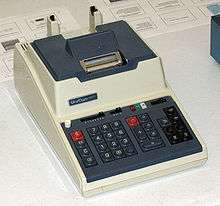
The first commercial product to use a microprocessor was the Busicom calculator 141-PF. The 4004 was also used in the first microprocessor-controlled pinball game, a prototype produced by Dave Nutting Associates for Bally in 1974.
According to Nick Tredennick, a microprocessor designer and expert witness to the Boone/Hyatt patent case:
Here are my opinions from [the] study [I conducted for the patent case]. The first microprocessor in a commercial product was the Four Phase Systems AL1. The first commercially available (sold as a component) microprocessor was the 4004 from Intel.
— [33]
A popular myth has it that Pioneer 10, the first spacecraft to leave the solar system, used an Intel 4004 microprocessor. According to Dr. Larry Lasher of Ames Research Center, the Pioneer team did evaluate the 4004, but decided it was too new at the time to include in any of the Pioneer projects. The myth was repeated by Federico Faggin himself in a lecture for the Computer History Museum in 2006.[34]
Legacy and value

Federico Faggin signed the 4004 with his initials because he knew that his silicon gate design embodied "the essence of the microprocessor". In a corner of the die you can read "F.F."[29]
On November 15, 2006, the 35th anniversary of the 4004, Intel celebrated by releasing the chip's schematics, mask works, and user manual.[35] A fully functional 41 x 58 cm,[36] 130x scale replica of the Intel 4004 was built using discrete transistors and put on display in 2006 at the Intel Museum in Santa Clara, California.[37]
On October 15, 2010, Faggin, Hoff, and Mazor were awarded the National Medal of Technology and Innovation by President Barack Obama for their pioneering work on the 4004.[38]
Notes
- ↑ although the early documentation states "0.75MHz", this is at odds with the timing diagrams which specify a minimum overall cycle time of 1350ns (=741kHz) and a maximum of 2010ns (=498kHz)
- ↑ This statistic comes from the same document as the "0.75MHz" claim and which appears to inaccurately round off the true figures for the purposes of summary. 850 µs with a minimum 10.8µs cycle time would in truth be 78.7 machine cycles, or roughly 629 clock ticks. As the processor is locked into an 8-tick cycle, it's more likely this operation would take 79 or even 80 full cycles, thus 632 to 640 ticks and 853 to 864 µs (or 854 to 865 µs at a true 740kHz), and reducing the actual execution speed to 1157 ~ 1172 (or 1156 ~ 1171) 8-digit additions per second
- ↑ However, this could only be used as working / data memory, and was non-executable: program code could not be stored in or run from RAM, as the processor kept the two memory areas strictly segregated at the microcode level. Instruction fetching forced assertion of the ROM chip-select line (and deassertion of the RAM select lines), and the chip had no way to "write" data to anything other than an IO port whilst the ROM area was selected.
- ↑ The only part of the 4004 memory space capable of storing executable code, though also usable for general purpose storage
References
- 1 2 "Intel 4004 Fun Facts". Intel.com. Retrieved 2011-07-06.
- ↑ http://www.intel.co.uk/content/www/uk/en/history/museum-story-of-intel-4004.html
- ↑ Faggin, F. (1992). "The Birth of the Microprocessor". Byte, pp. 145–150, March 1992.
- ↑ F. Faggin, T. Klein: "Silicon-Gate Technology". "Solid State Electronics", 1970, Vol. 13, pp. 1125–1144
- ↑ Faggin, Federico. "The New Methodology for Random Logic Design". Retrieved June 3, 2017.
- ↑ Faggin, Federico. "The Bootstrap Load". Retrieved June 3, 2017.
- ↑ Faggin, Federico. "The Buried Contact". Retrieved June 3, 2017.
- ↑ ""Inductee Detail"". National Inventors Hall of Fame. 2016-07-25.
- 1 2 Faggin, Federico. "The MOS Silicon Gate Technology and the First Microprocessors" (PDF). Rivista del Nuovo Cimento. 38 (12). Retrieved 2017-06-05.
- ↑ Woerner, Joerg (November 16, 2001). "The "Calculator-on-a-chip"". Datamath Calculator Museum. Retrieved 22 March 2016.
- ↑ Woerner, Joerg (February 26, 2001). "Texas Instruments: They invented the Microcontroller". Datamath Calculator Museum. Retrieved 22 March 2016.
- ↑ http://www.cpu-world.com/CPUs/4004/index.html Intel 4004 microprocessor family, retrieved 2011 Dec 14
- ↑ Gilder, George (1990). Microcosm: the quantum revolution in economics and technology. Simon and Schuster. p. 107. ISBN 978-0-671-70592-3.
Intel's first advertisement for the 4004 appeared in the November 15, 1971 issue of Electronic News
- ↑ Busicom Calculator Engineering Prototype (Gift of Federico Faggin to the Computer History Museum, Mountain View, California)
- 1 2 Faggin, Federico; Hoff, Marcian; Mazor, Stanley; Shima, Masatoshi (1996-12-01). "The history of the 4004". IEEE Micro. 16 (6): 10–20. doi:10.1109/40.546561.
- ↑ Inductee Detail National Inventors Hall of Fame
- ↑ Faggin, Federico. "Ted Hoff's Role in the Microprocessor". Retrieved June 3, 2017.
- ↑ Faggin, Federico. "A faster generation of MOS devices with low thresholds is riding the crest of the new wave, silicon-gate IC's". Retrieved June 3, 2017.
- ↑ Faggin, Federico. "Earliest Published Papers". Retrieved June 3, 2017.
- ↑ Possibly he had confused the Plessey name with that of Massey Ferguson, makers of agricultural machinery.
- ↑ "The Intel4004". Intel4004.com. Retrieved 2008-03-15.
- ↑ Nigel Tout. "The Busicom 141-PF calculator and the Intel 4004 microprocessor". Retrieved November 15, 2009.
- ↑ “Silicon Valley” by Moira Johnston, page 466, National Geographic, October 1982.
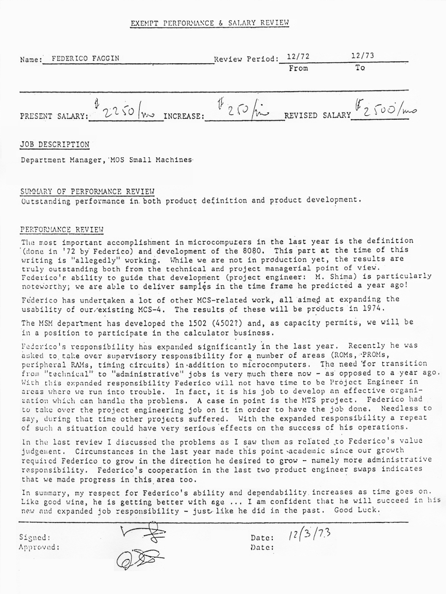
- ↑ Faggin, Federico. "Exempt performance and salary review'". Retrieved June 3, 2017.
- ↑ "History of Computing Industrial Era 1970 - 1971". 2010-10-19. Retrieved 2016-05-05.
In February Intel releases the 4004 microprocessor to the market. It has 12 sq mm die size and 16 pins which fit into a motherboard.
- ↑ "Intel 4004 datasheet" (PDF) (published 2010-07-06). 1987. Retrieved 2011-07-06.
- ↑ "Intel's Accidental Revolution". CNet.com. Archived from the original on 2012-07-11. Retrieved 2009-07-30.
- ↑ Hendrie, Gardner (2006). "Oral History of Federico Faggin" (PDF). Computer History Museum. Retrieved 2017-01-24.
- 1 2 "Federico Faggin's Signature". Intel4004.com. Retrieved 2012-08-21.
- ↑ Aspray, William (1994-05-25). "Oral-History: Tadashi Sasaki". Interview #211 for the Center for the History of Electrical Engineering. The Institute of Electrical and Electronics Engineers, Inc. Retrieved 2013-01-02.
- ↑ Intel's museum archive i4004 datasheet
- ↑ IMPORTANT section at page 25: http://www.intel.com/Assets/PDF/Manual/msc4.pdf
- ↑ "Dissertation 2004" (PDF). Retrieved 2017-11-14.
- ↑ "Intel 4004 Microprocessor 35th Anniversary". YouTube. Retrieved 2011-07-06.
- ↑ Intel 4004 Microprocessor Historical Materials, Intel Museum, 2009-11-15, accessed 2009-11-18
- ↑ "4004 @ 44: SVG Mask Artwork; New Busicom 141-PF replica PCB; Printer emulator". 2015-11-20. Retrieved 2016-05-05.
- ↑ "Intel 4004 -- 45th Anniversary Project". 2015-11-15. Retrieved 2016-04-02.
including fully functional 130x scale replicas of the 4004 built using discrete transistors, museum-durable keyboards and slide switches, and video display electronics.
- ↑ "President Obama Honors Nation's Top Scientists and Innovators" (Press release). October 15, 2010.
Patents
- US 3753011 August 14, 1973. Faggin, Federico: Power supply settable bi-stable circuit.
- US 3821715 June 28, 1974. Hoff, Marcian; Mazor, Stanley; Faggin, Federico: Memory system for multi-chip digital computer.
Historical documents
- Faggin F., Capocaccia F. "A New Integrated MOS Shift Register”, Proceedings XV International Electronics Scientific Congress, Rome, April 1968, pp. 143–152. This paper describes a novel static MOS shift register, developed at SGS-Fairchild (now ST Micro) at the end of 1967, before Federico Faggin joined Fairchild's R&D in Palo Alto (Ca) in February 1968. Faggin later used this new shift register in the MCS-4 chips, including the 4004.
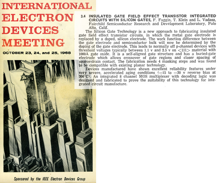
- Cover and abstract of the IEDM (International Electron Devices Meeting) Program (October 1968). The Silicon Gate Technology (SGT) was first presented by its developer, Federico Faggin, at the IEDM on October 23, 1968 in Washington, D.C. It was the only commercial process technology for the fabrication of MOS integrated circuits with self-aligned gate that was later universally adopted by the semiconductor industry. The SGT was the first technology to produce commercial dynamic RAMs, CCD image sensors, non volatile memories and the microprocessor, providing for the first time all the fundamental elements of a general purpose computer with LSI integrated circuits.
- Cover of Electronics Magazine (September 29, 1969). The Electronics article introduces the Fairchild 3708, designed by Federico Faggin in 1968. It was the world's first commercial integrated circuit using the Silicon Gate Technology, proving its viability.
- Initials F.F. (Federico Faggin) on the 4004 design (1971). The 4004 bears the initials F.F. of its designer, Federico Faggin, etched on one corner of the chip. Signing the chip was a spontaneous gesture of proud authorship and was also an original idea imitated after him by many Intel designers.
- Busicom 141-PF Printing Calculator Engineering Prototype (1971). (Gift of Federico Faggin to the Computer History Museum, Mountain View, CA). The CHM collection catalog shows pictures of the engineering prototype of the Busicom 141-PF desktop calculator. The engineering prototype used the world’s first microprocessor to have ever been produced. This one-of-a-kind prototype was a personal present by Busicom’s president Mr. Yoshio Kojima to Federico Faggin for his successful leadership of the design and development of the 4004 and three other memory and I/O chips (the MCS-4 chipset). After keeping it in his home for 25 years, Faggin donated it to the CHM in 1996.
- F. Faggin and M.E. Hoff: "Standard parts and custom design merge in four-chip processor kit". Electronics/April 24, 1972, pp. 112–116. Reprinted on pp. 6–27 to 6–31 of The Intel Memory Design Handbook: August 1973.
- F. Faggin, M. Shima, M.E. Hoff, Jr., H. Feeney, S. Mazor: "The MCS-4—An LSI micro computer system". IEEE '72 Region Six Conference. Reprinted on pp. 6–32 to 6–37 of The Intel Memory Design Handbook: August 1973.
Further reading
- Federico Faggin, Marcian E. Hoff Jr., Stanley Mazor and Masatoshi Shima. The history of the 4004. IEEE Micro, 16(6):10-20, December 1996. "The 4004 design team tells its story."
- Intel 4004 Microprocessor 35th Anniversary - Live recording of presentations by Ted Hoff and Federico Faggin at the Computer History Museum for the 35th anniversary of the first microprocessor. (youtube.com)
- IEEE Solid State Circuits Magazine, Winter 2009 Vol.1 No.1. "The 4004 microprocessor of Faggin, Hoff, Mazor, and Shima".
- The MOS Silicon Gate Technology and the First Microprocessors, by Federico Faggin published in La Rivista del Nuovo Cimento, Italian Physical Society, Vol. 38, No. 12, 2015.
- “How we made the microprocessor” by Federico Faggin. Nature Electronics, Vol. 1, January 2018. Published online: 8 January 2018
External links
- Intel's First Microprocessor—the Intel 4004: Intel Museum (Intel Corporate Archives) entry
- The Intel 4004: A testimonial from Federico Faggin, designer of the 4004 and developer of its enabling technology
- The New Methodology for Random Logic Design Used in the 4004 and in All the Early Intel Microprocessors
- Interview with Masatoshi Shima
- MCS-4 Micro Computer Set Data Sheet (12 pp)
- Intel 4004 -- 45th Anniversary Project, Schematics at the unofficial 4004 website, and a simulator in Java. Fully functional 130x scale replicas of the 4004 built using discrete transistors.
- The Crucial Role of Silicon Design in the Invention of the Microprocessor
- High resolution light microscope pictures of an Intel 4004 die together with a basic explanation of CMOS logic
- Intel 4004 Emulator, Assembler, and Disassembler: Simple programming tools for Intel 4004 in Javascript (Note this emulator currently has a bug: INC, which increments an index register, affects the carry flag, when in reality it should not.)
- Datasheet Intel 4004
- Datasheet Intel MCS-4
- BuscomV2p1 schematic
- MSC-4 Assembly Language Programming Manual
- Chip Hall of Fame: Intel 4004 Microprocessor (IEEE Spectrum website)