Intel 4040
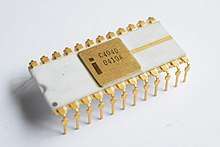 The ceramic C4040 variant. | |
| Produced | From 1974 to 1981[1] |
|---|---|
| Common manufacturer(s) |
|
| Max. CPU clock rate | 500 kHz to 740 kHz |
| Min. feature size | 10μm |
| Instruction set | 4-bit BCD oriented |
| Predecessor | Intel 4004 |
| Successor | none (Intel discontinued its 4-bit processors after the 4040.) |
| Package(s) |
|
The Intel 4040 microprocessor was the successor to the Intel 4004. It was introduced in 1974. The 4040 employed a 10 μm silicon gate enhancement load PMOS technology, was made up of 3,000 transistors[2] and could execute approximately 62,000 instructions per second. General performance, bus layout and instruction set was identical to the 4004, with the main improvements being in the addition of extra lines and instructions to recognise and service interrupts and hardware Halt/Stop commands (the latter allowing operator-controlled single-stepping for debugging purposes), an extended internal stack and general-purpose "Index" register space to handle nesting of several subroutines and/or interrupts, plus a doubling of program ROM address range.
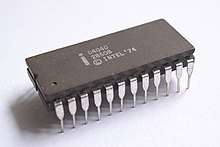 The ceramic D4040 variant. |
 The plastic P4040 variant. |
New features

- Interrupts
- Single Stepping plus both hardware and software HALTing.
- Low-power standby[Note 1]
Extensions
| Intel 4040 registers | ||||||||||||||||||||||||||||||||||||||||||||||||||||||||||||||||||||||||||||||||||||||||||||||||||||||||||||||||||||||||||||||||||||||||||||||||||||||||||||||||||||||||||||||||||||||||||||||||||||||||||||||||||||||||||||||||||||||||||||||||||||||||||||||||||||||||||||||||||||||||||||||||||||||||||||||||||||||||||||||||||||||||||||||||||||||||||||||||||||||||||||||||||||||||||||||||||||||||
| ||||||||||||||||||||||||||||||||||||||||||||||||||||||||||||||||||||||||||||||||||||||||||||||||||||||||||||||||||||||||||||||||||||||||||||||||||||||||||||||||||||||||||||||||||||||||||||||||||||||||||||||||||||||||||||||||||||||||||||||||||||||||||||||||||||||||||||||||||||||||||||||||||||||||||||||||||||||||||||||||||||||||||||||||||||||||||||||||||||||||||||||||||||||||||||||||||||||||
- Instruction Set expanded to 60 instructions (14 new instructions added to existing 46, mainly concerned with handling interrupts, halting/single stepping and ROM bank switching)
- Program memory (ROM) expanded to 8 KB (13-bit address space), using bank switching (4004's original single chip-select expanded to two mutually exclusive lines)[Note 2]
- Registers expanded to 24 (8 added to the 16 existing 4-bit-wide general-purpose "Index Register" set, mainly for use with interrupt processing)[Note 3]
- Subroutine/interrupt stack expanded to 7 levels deep (using dedicated internal registers)[Note 4]
Characteristics
- Data Bus: 4-bit
- Address Bus: 12-bit for ROM (multiplexed onto data bus; addresses took three bus cycles to transmit, same as in the 4004), effectively 13-bit with use of bank-switching commands; effectively 10-bit or 8-bit for RAM (8-bit direct address plus one-of-four, ie 2-bit equivalent, bank select; the additional 256 "status" memory locations required use of IO commands to read or write, from an overall 8-bit address space)
- Voltage: -15V DC
- Operating Frequency: 500 to 740 kHz main clock (2-phase, overlapping); 62500 to 92500 8-clock machine cycles per second, each instruction requiring either one or two machine cycles to read and execute, meaning a rough average of 62 kIPS at 740 kHz with an equal mix.[Note 5]
- Performance: Claimed approximate execution time of ~850 µs to add two 32-bit (8-digit BCD) numbers, or around 1175 such operations per second and approx 10 machine cycles per digit-pair.[Note 6]
Designers
Federico Faggin proposed the project, formulated the architecture and led the design. The detailed design was done by Tom Innes (Tinnes of Bristol).
New support chips
- 3216 and 3226 4-bit parallel bus drivers[Note 7]
- 4101 – 256 x 4-bit Static RAM[Note 8]
- 4201 – Clock Generator, 500 to 740 kHz, using 4.000 to 5.185 MHz crystals
- 4207 – General Purpose 8-bit Output port
- 4209 – General Purpose 8-bit Input port
- 4211 – General Purpose 8-bit I/O port
- 4265 - Programmable general-purpose I/O
- 4269 - Programmable keyboard/display
- 4289 – Standard Memory Interface (replaces 4008/4009)[Note 9]
- 4308 – 1K x 8-bit ROM plus 4 x 4-bit IO ports[Note 10]
- 4316 – 2K x 8-bit ROM[Note 11]
- 4702 – 256 x 8-bit EPROM[Note 12]
Production
Notes
- ↑ Essentially a side function of Halt/Single Step; all internal processing would be suspended, and most of the chip hardware put into a low-drain high-impedance condition, but the machine cycle clocks would be kept running for the benefit of external devices, including any interrupt controllers which would be needed to wake the chip back up, that relied on them to stay in sync.
- ↑ RAM space remained unchanged from the 4004, as did the inability to run programs from RAM
- ↑ Only 16 of the so-called "Index" registers (which operated and were usable in a way that would be more familiar as general purpose registers in a modern CPU, where an Index register has a much more specific application to memory addressing) could be accessed at any one time, with a particular bank switch command being required to swap-in one or other bank of 8 to logical registers 0-7, and registers 8-15 remaining continually accessible. The idea was that any mission-critical context should be kept in the first 8, as when an interrupt occurred it would not only push an exception handler address onto the stack but also switch Index Register banks, automatically preserving that state until the handler returned control to the normal program flow - assuming, of course, you hadn't already deliberately swapped banks in order to make use of the additional internal memory space. If an interrupt routine wanted to make use of the latter eight registers, it was up to the programmer to first save any data held in them to another location, and then restore it before returning from the routine.
- ↑ by default only one level of interrupt was supported, as further servicing was disabled once an initial interrupt was acknowledged and only re-enabled on RTI, essentially allowing three levels of subroutine stacking within an interrupt itself occurring within a three-deep subroutine, but detection could be forced back on with a specific command
- ↑ This may not be entirely accurate, and is based off the 4004 characteristics; some of the added instructions may require additional cycles to execute, especially any external register stacking required for interrupt handling, but it is not made clear in the documentation as to whether this is the case; halt/step are special cases which naturally take potentially many millions of cycles to "execute", but as these essentially occur "outside" of the usual program flow, they don't count for speed calculation.
- ↑ Likewise, based on claimed 4004 performance; "850 µs" is a somewhat rounded-off figure claimed in an early Intel brochure and may not be particularly precise, but the total execution time works out to approximately 79 or 80 machine cycles, which fits neatly with either 10 cycles per digit pair, 9 cycles per pair plus 7 for setup and any necessary post-processing, or 8 per pair plus 15 extra (...etc). The actual instruction mix wasn't specified, so without both source code and a list of instruction execution times it's impossible to be sure. A more efficient addition routine might have been possible on the 4040 vs the 4004, but the extra instructions don't suggest any obvious method for achieving this and appear to be focussed on addressing the earlier chip's more obvious shortcomings, e.g. a lack of interrupts and haltability.
- ↑ Provides "high" current (~25mA) handling capacity for external I/O devices. Allegedly intended solely for use with the 4289, but design appears fairly generic and may be adaptable to a bare 4004/4040?
- ↑ i.e. combining the main storage of four 4002s into a single individually-selectable chip, but with neither the 4-bit IO port nor additional 64 words of IO-command-accessed "status" memory. As it has a dedicated, 8-bit address bus, and two separate 4-bit data input and output buses, the 4101 is intended only for use as a downstream peripheral of the 4289. This is further emphasised by the SRAM's claim to be "used for writeable Program Memory", something not achievable by a bare 4004 or 4040.
- ↑ Allows connection of "standard" memory (8-bit parallel data and/or upto 12-bit parallel addressing, the latter in the form of 8-bit address plus 4-bit binary chip select) and devices to the 4004 or 4040, as well as the use of RAM as Program Memory (the 4289 can be installed so as to appear like a regular 4001 ROM to the processor regardless of what's connected on the other side; furthering the illusion, it also provides the same four I/O lines that a 4001 would offer). A 4040 making use of two 4289s could offer various combinations of ROM and RAM in 2KB segments up to 8KB total with a relatively simplistic segregated addressing scheme and a small number of 4101s and 4308s, e.g. 3x 4308 and 8x 4101 for 6KB ROM and 1KB RAM.
- ↑ Directly replaces four separate 4001s with a single chip, including being available in four "metal" variants that respond to logical chip addresses 0-3, 4-7, 8-11 and 12-15, simulating the sixteen original versions of the 4001
- ↑ Intended for use downstream of a 4289, as it presents an 11-bit parallel address input bus and separate 8-bit parallel data output bus, as well as three binary-coded chip select lines (thus allowing provision of upto 16KByte ROM with an addressing scheme incompatible with the 4004/4040 on several different levels - although only two 4316s, thus 4KBytes of ROM, or one 4316 plus RAM, can be directly addressed by a 4289 without additional hardware and/or special programming techniques)
- ↑ i.e. UV-erased rather than electronically, and is again intended for use with the 4289, as it has separate, 8-bit parallel, address input and data output buses