Kyropoulos process
The Kyropoulos process is a method of bulk crystal growth used to obtain single crystals. The process is named for Spyro Kyropoulos, who proposed the technique in 1926 as a method to grow brittle alkali halide and alkali earth metal crystals for precision optics.[1] [2]
The largest application is the growth of large boules of single crystal sapphire used in the electronics industry as a substrate used to manufacture gallium nitride-based LEDs, and in other industries as a durable optical material.[3]
Application
The Kyropoulos process (often referred to as the KY process) for sapphire crystal growth was developed in the 1970s in the Soviet Union. It is currently used by several companies around the world to produce sapphire for the electronics and optics industries.[4]
Production of Kyropoulos sapphire

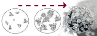
High-purity, aluminum oxide (only a few parts per million of impurities) is melted in a crucible at over 2100 degrees Celsius. Typically the crucible is made of tungsten or molybdenum. A precisely oriented seed crystal is dipped into the molten alumina. The seed crystal is slowly pulled upwards and may be rotated simultaneously. By precisely controlling the temperature gradients, rate of pulling and rate of temperature decrease, it is possible to produce a large, single-crystal, roughly cylindrical ingot from the melt. In contrast with the Czochralski process, the Kyropoulos process crystallizes the entire feedstock volume into the boule. The size and aspect ratio of the crucible is close to that of the final crystal, and the crystal grows downward into the crucible, rather than being pulled up and out of the crucible as in the Czochralski method. The upward pulling of the seed is at a much slower rate than the downward growth of the crystal, and serves primarily to shape the meniscus of the solid-liquid interface via surface tension. The growth rate is controlled by slowly decreasing the temperature of the furnace until the entire melt has solidified. Hanging the seed from a weight sensor can provide feedback to determine the growth rate, although precise measurements are complicated by the changing and imperfect shape of the crystal diameter, the unknown convex shape of the solid-liquid interface, and these features' interaction with buoyant forces and convection within the melt.[5] The Kyropoulos method is characterized by smaller temperature gradients at the crystallization front than the Czochralski method. Like the Czochralski method, the crystal grows free of any external mechanical shaping forces, and thus has few lattice defects and low internal stress.[3] This process can be performed in an inert atmosphere, such as argon, or under high vacuum.
Crystal sizes
The sizes of sapphire crystals grown by the Kyropoulos method have increased dramatically since the 1980s. In the mid-2000s sapphire crystals up to 30 kg were developed which could yield 150 mm diameter substrates. By 2017, the largest reported sapphire grown by the Kyropoulos method was 350 kg, and could produce 300 mm diameter substrates.[6] Because of sapphire's anisotropic crystal structure, the orientation of the cylindrical axis of the boules grown by the Kyropoulos process is perpendicular to the orientation required for deposition of GaN on the LED substrates.[7] This means that cores must be drilled through the sides of the boule before being sliced into wafers. This means the as-grown boules have a significantly larger diameter than the resulting wafers. As of 2017 the leading manufacturers of blue and white LEDs use 150 mm diameter sapphire substrates, with some manufacturers still using 100 mm, and 2 inch substrates.
See also
References
- ↑ "Evolution and Application of the Kyropoulos Crystal Growth Method", David F. Bliss, in "50 Years of Progress in Crystal Growth: A Reprint Collection", Ed. Robert Feigelson, Elsevier, 2005 ISBN 0080489931
- ↑ Kyropoulos, S. (1926). "Ein Verfahren zur Herstellung großer Kristalle". Zeitschrift für anorganische und allgemeine Chemie (in German). 154: 308–313. doi:10.1002/zaac.19261540129.
- 1 2 Dobrovinskaya, Elena R., Leonid A. Lytvynov, and Valerian Pishchik. Sapphire: material, manufacturing, applications. Springer Science & Business Media, 2009. ISBN 0387856943
- ↑ "Status Of the Sapphire Industry." Eric Virey. Yole-CIOE Sapphire Forum, Shenzhen, August 31st 2015. Yole Development. p. 32.
- ↑ Winkler, Jan; Neubert, Michael (2015). "Automation of Crystal Growth from Melt". In Rudolph, Peter. Handbook of Crystal Growth (2nd ed.). Elsevier B.V. pp. 1176–1178.
- ↑ "Monocrystal introduced world's first 350 kg KY sapphire crystal" (PDF). Monocrystal. Retrieved 16 January 2018.
- ↑ Tang, Huili; Li, Hongjun; Xu, Jun (2013). "Growth and Development of Sapphire Crystal for LED Applications". In Ferreira, Sukarno. Advanced Topics on Crystal Growth. InTech.