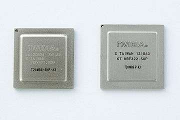
Tegra
Tegra is a system on a chip (SoC) series developed by Nvidia for mobile devices such as smartphones, personal digital assistants, and mobile Internet devices. The Tegra integrates an ARM architecture central processing unit (CPU), graphics processing unit (GPU), northbridge, southbridge, and memory controller onto one package. Early Tegra SoCs are designed as efficient multimedia processors, while more recent models emphasize performance for gaming and machine learning applications, without sacrificing power efficiency.[1]
History
The Tegra APX 2500 was announced on February 12, 2008. The Tegra 6xx product line was revealed on June 2, 2008,[2] and the APX 2600 was announced in February 2009. The APX chips were designed for smartphones, while the Tegra 600 and 650 chips were intended for smartbooks and mobile Internet devices (MID).[3]
The first product to use the Tegra was Microsoft's Zune HD media player in September 2009, followed by the Samsung M1.[4] Microsoft's Kin was the first cellular phone to use the Tegra;[5] however, the phone did not have an app store, so the Tegra's power did not provide much advantage. In September 2008, Nvidia and Opera Software announced that they would produce a version of the Opera 9.5 browser optimised for the Tegra on Windows Mobile and Windows CE.[6][7] At Mobile World Congress 2009, Nvidia introduced its port of Google's Android to the Tegra.
On January 7, 2010, Nvidia officially announced and demonstrated its next generation Tegra system-on-a-chip, the Nvidia Tegra 250, at Consumer Electronics Show 2010.[8] Nvidia primarily supports Android on Tegra 2, but booting other ARM-supporting operating systems is possible on devices where the bootloader is accessible. Tegra 2 support for the Ubuntu GNU/Linux distribution was also announced on the Nvidia developer forum.[9]
Nvidia announced the first quad-core SoC at the February 2011 Mobile World Congress event in Barcelona. Though the chip was codenamed Kal-El, it is now branded as Tegra 3. Early benchmark results show impressive gains over Tegra 2,[10][11] and the chip was used in many of the tablets released in the second half of 2011.
In January 2012, Nvidia announced that Audi had selected the Tegra 3 processor for its In-Vehicle Infotainment systems and digital instruments display.[12] The processor will be integrated into Audi's entire line of vehicles worldwide, beginning in 2013. The process is ISO 26262-certified.[13]
In summer of 2012 Tesla Motors began shipping the Model S all electric, high performance sedan, which contains two NVIDIA Tegra 3D Visual Computing Modules (VCM). One VCM powers the 17-inch touchscreen infotainment system, and one drives the 12.3-inch all digital instrument cluster."[14]
In March 2015, Nvidia announced the Tegra X1, the first SoC to have a graphics performance of 1 teraflop. At the announcement event, Nvidia showed off Epic Games' Unreal Engine 4 "Elemental" demo, running on a Tegra X1.
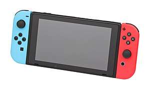
On October 20, 2016, Nvidia announced that Nintendo's then upcoming Switch hybrid home/portable game console will be powered by Tegra hardware.[15] On March 15, 2017, TechInsights revealed the Nintendo Switch is powered by a custom Tegra X1 (model T210), with lower clockspeeds.[16]
Specifications
Tegra APX
- Tegra APX 2500
- Processor: ARM11 600 MHz MPCore (originally GeForce ULV)
- Suffix: APX (formerly CSX)
- Memory: NOR or NAND flash, Mobile DDR
- Graphics: Image processor (FWVGA 854×480 pixels)
- Up to 12 megapixels camera support
- LCD controller supports resolutions up to 1280×1024
- Storage: IDE for SSD
- Video codecs: up to 720p MPEG-4 AVC/H.264 and VC-1 decoding
- Includes GeForce ULV support for OpenGL ES 2.0, Direct3D Mobile, and programmable shaders
- Output: HDMI, VGA, composite video, S-Video, stereo jack, USB
- USB On-The-Go
- Tegra APX 2600
- Enhanced NAND flash
- Video codecs:[17]
- 720p H.264 Baseline Profile encode or decode
- 720p VC-1/WMV9 Advanced Profile decode
- D-1 MPEG-4 Simple Profile encode or decode
Tegra 6xx
- Tegra 600
- Targeted for GPS segment and automotive
- Processor: ARM11 700 MHz MPCore
- Memory: low-power DDR (DDR-333, 166 MHz)
- SXGA, HDMI, USB, stereo jack
- HD camera 720p
- Tegra 650
- Targeted for GTX of handheld and notebook
- Processor: ARM11 800 MHz MPCore
- Low power DDR (DDR-400, 200 MHz)
- Less than 1 watt envelope
- HD image processing for advanced digital still camera and HD camcorder functions
- Display supports 1080p at 24 frame/s, HDMI v1.3, WSXGA+ LCD and CRT, and NTSC/PAL TV output
- Direct support for Wi-Fi, disk drives, keyboard, mouse, and other peripherals
- A complete board support package (BSP) to enable fast time to market for Windows Mobile-based designs
Tegra 2

The second generation Tegra SoC has a dual-core ARM Cortex-A9 CPU, an ultra low power (ULP) GeForce GPU,[18] a 32-bit memory controller with either LPDDR2-600 or DDR2-667 memory, a 32KB/32KB L1 cache per core and a shared 1MB L2 cache.[19] Tegra 2's Cortex A9 implementation does not include ARM's SIMD extension, NEON. There is a version of the Tegra 2 SoC supporting 3D displays; this SoC uses a higher clocked CPU and GPU.
The Tegra 2 video decoder is largely unchanged from the original Tegra and has limited support for HD formats.[20] The lack of support for high-profile H.264 is particularly troublesome when using online video streaming services.
Common features:
- CPU cache: L1: 32 KB instruction + 32 KB data, L2: 1 MB
- 40 nm semiconductor technology
| Model number |
CPU | GPU | Memory | Adoption | |||||||
|---|---|---|---|---|---|---|---|---|---|---|---|
| Processor | Cores | Frequency | Micro- architecture |
Core configuration1 |
Frequency | Type | Amount | Bus width |
Band- width |
Availability | |
| AP20H (Ventana/Unknown) | Cortex-A9 | 2 | 1.0 GHz | VLIW-based VEC4 units[21] | 4:4:?:? | 300 MHz | LPDDR2 300 MHz DDR2 333 MHz | ? | 32 bit single-channel | 2.4 GB/s 2.7 GB/s |
Q1 2010 |
| T20 (Harmony/Ventana) | 333 MHz | ||||||||||
| AP25 | 1.2 GHz | 400 MHz | Q1 2011 | ||||||||
| T25 | |||||||||||
Devices
| Model | Devices |
|---|---|
| AP20H | Motorola Atrix 4G, Motorola Droid X2, Motorola Photon, LG Optimus 2X / LG Optimus Dual P990 / Optimus 2x SU660 (?), Samsung Galaxy R, Samsung Captivate Glide, T-Mobile G2X P999, Acer Iconia Tab A200 and A500, LG Optimus Pad, Motorola Xoom,[22] Sony Tablet S, Dell Streak Pro[23], Toshiba Thrive[24] tablet, T-Mobile G-Slate |
| T20 | Avionic Design Tamonten Processor Board,[25] Notion Ink Adam tablet, Olivetti OliPad 100, ViewSonic G Tablet, ASUS Eee Pad Transformer, Samsung Galaxy Tab 10.1, Toshiba AC100, CompuLab Trim-Slice nettop, Velocity Micro Cruz Tablet L510, Acer Iconia Tab A100 |
| AP25 | Fusion Garage Grid 10 |
| Unknown | Tesla Motors models 2013~2014 instrument cluster (IC)[26][27] |
Tegra 3
NVIDIA's Tegra 3 (codenamed "Kal-El")[28] is functionally a SoC with a quad-core ARM Cortex-A9 MPCore CPU, but includes a fifth "companion" core in what Nvidia refers to as a "variable SMP architecture".[29] While all cores are Cortex-A9s, the companion core is manufactured with a low-power silicon process. This core operates transparently to applications and is used to reduce power consumption when processing load is minimal. The main quad-core portion of the CPU powers off in these situations.
Tegra 3 is the first Tegra release to support ARM's SIMD extension, NEON.
The GPU in Tegra 3 is an evolution of the Tegra 2 GPU, with 4 additional pixel shader units and higher clock frequency. It can also output video up to 2560×1600 resolution and supports 1080p MPEG-4 AVC/h.264 40 Mbit/s High-Profile, VC1-AP, and simpler forms of MPEG-4 such as DivX and Xvid.[30]
The Tegra 3 was released on November 9, 2011.[31]
Common features:
- CPU cache: L1: 32 KB instruction + 32 KB data, L2: 1 MB
- 40 nm LPG semiconductor technology by TSMC
| Model number |
CPU | GPU | Memory | Adoption | |||||||
|---|---|---|---|---|---|---|---|---|---|---|---|
| Processor | Cores | Frequency (multi- / single-core mode) |
Micro- architecture |
Core configuration1 |
Frequency | Type | Amount | Bus width |
Band- width |
Availability | |
| T30L | Cortex-A9 | 4+1 | 1.2 GHz / up to 1.3 GHz | VLIW-based VEC4 units[21] | 8:4:?:? | 416 MHz | DDR3-1333 | ? | 32 bit single-channel | 5.3 GB/s[32] | Q1 2012 |
| T30 | 1.4 GHz / up to 1.5 GHz | 520 MHz | LPDDR2-1066 DDR3-L-1500 | ? | 4.3 GB/s 6.0 GB/s[33] |
Q4 2011 | |||||
| AP33 | |||||||||||
| T33 | 1.6 GHz / up to 1.7 GHz[32] | DDR3-1600 | ? | 6.4 GB/s[32] | Q2 2012 | ||||||
Devices
| Model | Devices |
|---|---|
| T30L | Asus Transformer Pad TF300T, Microsoft Surface, Nexus 7 (2012),[34] Sony Xperia Tablet S, Acer Iconia Tab A210, Toshiba AT300 (Excite 10),[35] BLU Quattro 4.5,[36] |
| T30 | Asus Eee Pad Transformer Prime,[37] IdeaTab K2 / LePad K2,[38] Acer Iconia Tab A510, Fuhu Inc. nabi 2 Tablet,[39] Tesla Motors models 2013~2014 center information display (CID),[26][27] Tesla Model S of 2015 instrument cluster (IC),[40] Microsoft Surface,[41] Lenovo IdeaPad Yoga 11,[42][43] |
| AP33 | LG Optimus 4X HD, HTC One X, XOLO Play T1000,[44] |
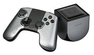
| T33 | Asus Transformer Pad Infinity (TF700T), Fujitsu ARROWS X F-02E, Ouya, HTC One X+ |
Tegra 4
The Tegra 4 (codenamed "Wayne") was announced on January 6, 2013 and is a SoC with a quad-core CPU, but includes a fifth low-power Cortex A15 companion core which is invisible to the OS and performs background tasks to save power. This power-saving configuration is referred to as "variable SMP architecture" and operates like the similar configuration in Tegra 3.[45]
The GeForce GPU in Tegra 4 is again an evolution of its predecessors. However, numerous feature additions and efficiency improvements were implemented. The number of processing resources was dramatically increased, and clock rate increased as well. In 3D tests, the Tegra 4 GPU is typically several times faster than that of Tegra 3.[46] Additionally, the Tegra 4 video processor has full support for hardware decoding and encoding of WebM video (up to 1080p 60Mbit/s @ 60fps).[47]
Along with Tegra 4, Nvidia also introduced i500, an optional software modem based on Nvidia's acquisition of Icera, which can be reprogrammed to support new network standards. It supports category 3 (100Mbit/s) LTE but will later be updated to Category 4 (150Mbit/s).
Common features:
- CPU cache: L1: 32 KB instruction + 32 KB data, L2: 2 MB
- 28 nm HPL semiconductor technology
| Model number |
CPU | GPU | Memory | Adoption | |||||||
|---|---|---|---|---|---|---|---|---|---|---|---|
| Processor | Cores | Frequency | Microarchitecture | Core configuration1 |
Frequency | Type | Amount | Bus width |
Band- width |
Availability | |
| T114[48] | Cortex-A15 | 4+1 | up to 1.9 GHz | VLIW-based VEC4 units[49] | 72 (48:24:4)[21][49] | 672 MHz[50] | DDR3L or LPDDR3 | ? | 32 bit dual-channel | up to 14.9 GB/s (1866 MT/s data rate)[51][52] | Q2 2013[53] |
1 Pixel shaders : Vertex shaders : Pixel pipelines
Devices
| Model | Devices |
|---|---|
| T114 | Nvidia Shield Portable, Tegra Note 7, Microsoft Surface 2, HP Slate 7 Extreme,[54] HP Slate 7 Beats Special Edition,[55] HP Slate 8 Pro,[56] HP SlateBook x2,[57] HP SlateBook 14,[58] HP Slate 21,[59] ZTE N988S, nabi Big Tab, Nuvola NP-1, Project Mojo, Asus Transformer Pad TF701T, Toshiba AT10-LE-A (Excite Pro), Vizio 10" tablet, Wexler.Terra 7, Wexler.Terra 10, Acer TA272HUL AIO, Xiaomi Phone 3,[60] Coolpad 大观 4,[61] Audi Tablet,[62] Le Pan TC1020 10.1",[63] Matrimax iPLAY 7,[64] Kobo Arc 10HD,[65] Tesla Model S of 2015 center information display (CID)[40] |
Tegra 4i
The Tegra 4i (codenamed "Grey") was announced on February 19, 2013. With hardware support for the same audio and video formats,[47] but using Cortex-A9 cores instead of Cortex-A15, the Tegra 4i is a low-power variant of the Tegra 4 and is designed for phones and tablets. Unlike its Tegra 4 counterpart, the Tegra 4i also integrates the Icera i500 LTE/HSPA+ baseband processor onto the same die.
Common features:
- 28 nm HPM semiconductor technology
- CPU cache: L1: 32 KB instruction + 32 KB data, L2: 1 MB
| Model number |
CPU | GPU | Memory | Adoption | |||||||
|---|---|---|---|---|---|---|---|---|---|---|---|
| Processor | Cores | Frequency | Microarchitecture | Core configuration1 |
Frequency | Type | Amount | Bus width |
Band- width |
Availability | |
| T148?[66] | Cortex-A9 "R4" | 4+1 | up to 2.0 GHz | VLIW-based VEC4 units[49] | 60 (48:12:2)[49] | 660 MHz[50] | LPDDR3 | 32 bit single-channel | 6.4–7.5 GB/s (800–933 MHz)[52] | Q1 2014 | |
1 Pixel shaders : Vertex shaders : Pixel pipelines
Devices
| Model | Devices |
|---|---|
| T148? | Blackphone, LG G2 mini LTE, Wiko Highway 4G,[67] Explay 4Game,[68] Wiko Wax[69][70] QMobile Noir LT-250[71] |
Tegra K1
Nvidia’s Tegra K1 (codenamed "Logan") features ARM Cortex-A15 cores in a 4+1 configuration similar to Tegra 4, or Nvidia's 64-bit Project Denver dual-core processor as well as a Kepler graphics processing unit with support for Direct3D 12, OpenGL ES 3.1, CUDA 6.5, OpenGL 4.4/OpenGL 4.5, and Vulkan.[72][73] Nvidia claims that it outperforms both the Xbox 360 and the PS3, whilst consuming significantly less power.[74]
Support Adaptive Scalable Texture Compression.[75]
In late April 2014, Nvidia shipped the "Jetson TK1" development board containing a Tegra K1 SoC and running Ubuntu Linux.[76]
- Processor:
- 32-bit variant quad-core ARM Cortex-A15 MPCore R3 + low power companion core
- or 64-bit variant with dual-core Project Denver[77] (variant once codenamed "Stark"[78])
- GPU consisting of 192 ALUs using Kepler technology
- 28 nm HPM process
- Released in Q2 2014
- Power consumption: 8 watts[74]
| Model number |
CPU | GPU | Memory | Adoption | ||||||||
|---|---|---|---|---|---|---|---|---|---|---|---|---|
| Processor | Cores | Frequency | Micro- architecture |
Core configuration1 |
Frequency | GFLOPS (FP32) |
Type | Amount | Bus width |
Band- width |
Availability | |
| T124[79] | Cortex-A15 R3 (32-bit) |
4+1 | up to 2.3 GHz[80] | GK20A (Kepler) |
192:8:4[81] | 756–951 MHz | 290–365[82] | DDR3L LPDDR3[81] |
max 8 GB with 40-bit address extension2 |
64 bit | 17 GB/s[81] | Q2 2014 |
| T132 | Denver (64-bit) |
2[81] | up to 2.5 GHz[80] | max 8 GB | ? | ? | Q3 2014 | |||||
1 Unified Shaders : Texture mapping units : Render output units
2 ARM Large Physical Page Extension (LPAE) supports 1 TiB (240 bytes). The 8 GiB limitation is part-specific.
Devices
| Model | Devices |
|---|---|
| T124 | Jetson TK1 development board,[83] Nvidia Shield Tablet,[84] Acer Chromebook 13,[85] HP Chromebook 14 G3,[86] Xiaomi MiPad,[87] Snail Games OBox, UTStarcom MC8718, Google Project Tango tablet,[88] Apalis TK1 System on Module,[89] Fuze Tomahawk F1,[90] JXD Singularity S192[91] |
| T132 | HTC Nexus 9[92][93] |
In December 2015, the web page of wccftech.com published an article stating that Tesla is going to use a Tegra K1 based design derived from the template of the Nvidia Visual Computing Module (VCM) for driving the infotainment systems and providing visual driving aid in the respective vehicle models of that time.[94] This news has, as of now, found no similar successor or other clear confirmation later on in any other place on such a combination of a multimedia with an auto pilot system for these vehicle models.
Tegra X1
Nvidia's Tegra X1 (codenamed "Erista") features four ARM Cortex-A57 cores and four unused ARM Cortex-A53 cores, as well as a Maxwell-based graphics processing unit.[95][96] It supports Adaptive Scalable Texture Compression.[75] Contrary to initial belief, Nvidia does not use the eight cores in ARM big.LITTLE configuration. Instead, devices utilizing the Tegra X1 always show themselves as having only four ARM Cortex-A57 cores available. The other four ARM Cortex-A53 cores cannot be accessed by the operating system, are unused in known devices, and have been removed by Nvidia from later versions of technical documentation, implying that a silicon erratum prevents their normal usage.[97][98]
A revision with faster clock speeds, known officially as Tegra X1+ was released in 2019.[99] It's also known as T214, Mariko and T210B01.
- CPU: ARMv8 ARM Cortex-A57 quad-core (64-bit) + (unused?) ARM Cortex-A53 quad-core (64-bit)
- GPU: Maxwell-based 256 core GPU (Jetson Nano: only 128 cores)
- MPEG-4 HEVC & VP9 encoding/decoding support[100] (Jetson Nano: encoders are H.265, H.264/Stereo, VP8, JPEG; decoders are H.265, H.264/Stereo, VP8, VP9, VC-1, MPEG-2, JPEG)
- TSMC 20 nm process for the Tegra X1, TSMC 16 nm process for the Tegra X1+.
- TDP:
- The chip used on the Jetson Nano module is the TM660M[103]
| Model number |
Process | CPU | GPU | Memory | Adoption | |||||||||
|---|---|---|---|---|---|---|---|---|---|---|---|---|---|---|
| Processor | Cores | Frequency | Micro- architecture |
Core configuration1 |
Frequency | GFLOPS (FP32) |
GFLOPS (FP16) |
Type | Amount | Bus width |
Band- width |
Availability | ||
| T210 | TSMC 20nm | Cortex-A57 + Cortex-A53[104]:753 |
A57: 4 A53: 4[104] |
A57: 1.9 GHz A53: 1.3 GHz |
GM20B (Maxwell)[104]:14 |
256:[104]16:16 | 1000 MHz | 512 | 1024 | LPDDR3/LPDDR4 | 8 GB[104] | 64 bit[104] | 25.6 GB/s | Q2 2015 |
| T214 | TSMC 16nm | 1267 MHz[105] | 649 | 1298 | LPDDR4/LPDDR4X | Q2 2019 | ||||||||
| TM660M | ? | Cortex-A57 | 4 | 1.428 GHz | GM20B (Maxwell) |
128:16:16 | 921 MHz | 236 | 472 | LPDDR3?/LPDDR4:773 | 4 GB (8?) | 64 bit | March 2019 | |
Devices
| Model | Devices |
|---|---|
| T210 | Nvidia Shield Android TV (2015 & 2017), Nvidia Jetson TX1 development board,[106] Nvidia Drive CX & PX, Google Pixel C, Nintendo Switch (2017)[107][16] |
| T214 | Nvidia Shield Android TV (2019), Nintendo Switch (2019 model, HAC-001(-01)), Nintendo Switch Lite |
| TM660M | Jetson Nano |
Tegra X2
Nvidia's Tegra X2[108][109] (codenamed "Parker") features Nvidia's own custom general-purpose ARMv8-compatible core Denver 2 as well as code-named Pascal graphics processing core with GPGPU support.[110] The chips are made using FinFET process technology using TSMC's 16 nm FinFET+ manufacturing process.[111][112][113]
- CPU: Nvidia Denver2 ARMv8 (64-bit) dual-core + ARMv8 ARM Cortex-A57 quad-core (64-bit)
- RAM: up to 8GB LPDDR4[114]
- GPU: Pascal-based, 256 CUDA cores
- TSMC 16 nm, FinFET process
- TDP: 7.5–15 W[115]
| Model number |
CPU | GPU | Memory | Adoption | |||||||||
|---|---|---|---|---|---|---|---|---|---|---|---|---|---|
| Processor | Cores | Frequency | Micro- architecture |
Core configuration1 |
Frequency | GFLOPS (FP32) |
GFLOPS (FP16) |
Type | Amount | Bus width |
Band- width |
Availability | |
| T186 | Denver2 + Cortex-A57 |
2 + 4 | Denver2: 1.4–2.0 GHz A57: 1.2–2.0 GHz |
GP10B (Pascal)[116] | 256:?:? | 854–1465 MHz | 437–750 | 874–1500 | LPDDR4 | 8 GB | 128 bit | 59.7 GB/s | |
Devices
| Model | Devices |
|---|---|
| T186 | Nvidia Drive PX2 (variants), ZF ProAI 1.1[117] |
| Unknown | Nvidia Jetson TX2[115] |
| Unknown | Mercedes-Benz MBUX (infotainment system)[118] |
| Unknown | 1 unit along with 1 GPU semiconductor is part of the ECU for "Tesla vision" functionality in all Tesla vehicles since October 2016[119][120] |
| Unknown | Magic Leap One[121][122] (mixed environment glasses) |
| Unknown | Skydio 2 (drone)[123] |
Xavier
The most recent Tegra SoC, Xavier, named after the comic book character Professor X, was announced on 28 September 2016, and by March 2019, it had been released.[124] It contains 7 billion transistors and 8 custom ARMv8 cores, a Volta GPU with 512 CUDA cores, an open sourced TPU (Tensor Processing Unit) called DLA (Deep Learning Accelerator)[125][126] It is able to encode and decode 8K Ultra HD (7680×4320). Users can configure operating modes at 10 W, 15 W, and 30 W TDP as needed and the die size is 350 mm2.[127][128][129] Nvidia confirmed the fabrication process to be 12 nm FinFET at CES 2018.[130]
- CPU: Nvidia custom Carmel ARMv8.2-A (64-bit), 8 cores 10-wide superscalar[131]
- GPU: Volta-based, 512 CUDA cores with 1.4 TFLOPS[132]
- TSMC 12 nm, FinFET process[130]
- 20 TOPS DL and 160 SPECint @ 20 W;[127] 30 TOPS DL @ 30 W[129] (TOPS DL = Deep Learning Tera-Ops)
- 20 TOPS DL via the GPU based tensor cores
- 10 TOPS DL (INT8) via the DLA unit that shall achieve 5 TFLOPS (FP16)[132]
- 1.6 TOPS in the PVA unit (Programmable Vision Accelerator,[133] for StereoDisparity/OpticalFlow/ImageProcessing)
- 1.5 GPix/s in the ISP unit (Image Signal Processor, with native full-range HDR and tile processing support)
- Video processor for 1.2 GPix/s encoding and 1.8 GPix/s decode[132] including 8k video support[134]
- MIPI-CSI-3 with 16 lanes[135][136]
- 1 Gbit/s Ethernet
- 10 Gbit/s Ethernet
| Model number |
CPU | GPU | Memory | Adoption | |||||||||
|---|---|---|---|---|---|---|---|---|---|---|---|---|---|
| Processor | Cores | Frequency | Micro- architecture |
Core configuration1 |
Frequency | GFLOPS (FP32) |
GFLOPS (FP16) |
Type | Amount | Bus width |
Band- width |
Availability | |
| T194[137] | Carmel | 8 | up to 2.26 GHz | GV10B?[138] (Volta) | 512:32:16 | 854–1377 MHz | 874–1410 | 1748–2820 | LPDDR4X | 16 GB | 256-bit | 137 GB/s | March 2019 |
| NX (15W) | Carmel | 2, 4 or 6 | up to 1.4 GHz (Hexa and Quad Core) or up to 1.9 GHz (Dual Core) | (Volta) | 384:?:? | 1100 MHz | 845 | 1690 | LPDDR4X | 8 GB | 128-bit | 51.2 GB/s | March 2020 |
| NX (10W) | Carmel | 2 or 4 | up to 1.2 GHz (Quad Core) or up to 1.5 GHz (Dual Core) | (Volta) | 384:?:? | 800 MHz | 614 | 1229 | LPDDR4X | 8 GB | 128-bit | 51.2 GB/s | March 2020 |
Devices
| Model | Devices |
|---|---|
| Unknown | Nvidia Drive Xavier (Drive PX-series)[139] (formerly named Xavier AI Car Supercomputer) |
| Unknown | Nvidia Drive Pegasus (Drive PX-series)[139] |
| Unknown | Nvidia Drive AGX Xavier Developer Kit[140] |
| Unknown | Nvidia Jetson AGX Xavier Developer Kit[141] |
| Unknown | Nvidia Jetson Xavier[142] |
| Unknown | Nvidia Jetson Xavier NX[143] |
| Unknown | Nvidia Clara AGX[144] "Clara AGX is based on NVIDIA Xavier and NVIDIA Turing GPUs."[145] |
| Unknown | Bosch and Nvidia designed Self Driving System[146] |
| Unknown | ZF ProAI[147][148] |
On the Linux Kernel Mailing List, a Tegra194 based development board with type ID "P2972-0000" got reported: The board consists of the P2888 compute module and the P2822 baseboard.[149]
Orin
Nvidia announced the next-gen SoC codename Orin (resembling the name of a character from the Aquaman franchise[150]) on March 27, 2018 at GPU Technology Conference 2018.[151] The Drive AGX Orin family was announced on December 18, 2019 at GTC China 2019. It contains 17 billion transistors and 12 Arm Hercules cores and is capable of 200 INT8 TOPs @ 65W.[152]
- CPU: 12x Arm Cortex-A78 (Hercules) ARMv8.2-A (64-bit)
- GPU: Ampere-based, ? CUDA cores with ? TFLOPS
- 200 TOPS DL
- ? TOPS DL (INT8) via the GPU based tensor cores
- ? TOPS DL (INT8) via the DLA unit
- 5 TOPS in the PVA unit (Programmable Vision Accelerator for Feature Tracking
- ? GPix/s in the ISP unit (Image Signal Processor, with native full-range HDR and tile processing support)
- Video processor for ? GPix/s encoding and ? GPix/s decode
- 4x 10 Gbit/s Ethernet
| Model number |
CPU | GPU | Memory | Adoption | |||||||||
|---|---|---|---|---|---|---|---|---|---|---|---|---|---|
| Processor | Cores | Frequency | Micro- architecture |
Core configuration1 |
Frequency | GFLOPS (FP32) |
GFLOPS (FP16) |
Type | Amount | Bus width |
Band- width |
Availability | |
| ? | Cortex-A78 (Hercules) | 12 | up to ? GHz | Ampere | ?:?:? | ? MHz | ? | ? | LPDDR5? | ? GB | 256-bit? | 200 GB/s | 2021? |
Models comparison
| Series/ Generation |
Tegra 2 | Tegra 3 | Tegra 4 | Tegra 4i | Tegra K1 | Tegra X1 | Tegra X2 | Xavier | Orin | ||
|---|---|---|---|---|---|---|---|---|---|---|---|
| Model/Device | all | all | all | T148? | T124 | T132 | T210 | T186 | T194 | ? | |
| CPU | Instruction set | ARMv7-A (32 bit) | ARMv8-A (64 bit) | ARMv8.2-A (64 bit) | ARMv8.2-A (64 bit) | ||||||
| Cores | 2 A9 | 4+1 A9 | 4+1 A15 | 4+1 A9 | 4+1 A15 | 2 Denver | 4 A53 + 4 A57 | 2 Denver2 + 4 A57 | 8 Nvidia Carmel | 12 Arm Cortex-A78 (Hercules) | |
| L1 Cache (I / D) | 32 / 32 KB | 128 / 64 KB | 32 / 32 KB + 64 / 32 KB | 128 / 64 KB + 48 / 32 KB | 64 / 64 KB | ? | |||||
| L2 Cache | 1 MB | 2 MB | 128 KB + 2 MB | 2 MB + 2 MB | 8 MB | ? | |||||
| L3 Cache | NA | 4 MB | ? | ||||||||
| GPU | Architecture | Vec4 | Kepler | Maxwell | Pascal | Volta | Ampere | ||||
| CUDA Cores | 4+4* | 8+4* | 48+24* | 48+12* | 192 | 256 | 512 | ? | |||
| RAM | Protocol | DDR2 | DDR3/DDR2 | DDR3 | LPDDR3/LPDDR4 | LPDDR4/LPDDR4X | LPDDR5? | ||||
| Max. size | 1 GB | 2 GB | 4 GB | 4 GB | 8 GB | 8 GB | 8 GB | 32 GB | ? | ||
| Bandwidth | 2.7 GB/s | 6.4 GB/s | 7.5 GB/s | 14.88 GB/s | 25.6 GB/s | 59.7 GB/s | 136.5 GB/s | 200 GB/s | |||
| Process | 40 nm | 28 nm HPL | 28 nm HPM | 20 nm SOC | 16 nm FF | 12 nm FFN | ? | ||||
* VLIW-based Vec4: Pixel shaders + Vertex shaders. Since Kepler, Unified shaders are used.
Software support
Linux
Nvidia distributes proprietary device drivers for Tegra through OEMs and as part of its "Linux for Tegra" (formerly "L4T") development kit. The newer and more powerful devices of the Tegra family are now supported by Nvidia's own Vibrante Linux distribution. Vibrante comes with a larger set of GNU/Linux tools plus several Nvidia provided libraries for acceleration in the area of data processing and especially image processing for driving safety and automated driving up to the level of deep learning and neuronal networks that make e.g. heavy use of the CUDA capable accelerator blocks, and via OpenCV can make use of the NEON vector extensions of the ARM cores.
As of April 2012, due to different "business needs" from that of their GeForce line of graphics cards, Nvidia and one of their Embedded Partners, Avionic Design GmbH from Germany, are also working on submitting open-source drivers for Tegra upstream to the mainline Linux kernel.[153][154] Nvidia co-founder & CEO laid out the Tegra processor roadmap using Ubuntu Unity in GPU Technology Conference 2013.[155]
By end of 2018 its evident that Nvidia employees have contributed substantial code parts to make the T186 and T194 models run for HDMI display and audio with the upcoming official Linux kernel 4.21 in about Q1 2019. The thus positively affected software modules are the open source Nouveau and the closed source Nvidia graphics drivers along with the Nvidia proprietary CUDA interface.[156]
Similar platforms
SoCs and platforms with comparable specifications (e.g. audio/video input, output and processing capability, connectivity, programmability, entertainment/embedded/automotive capabilities & certifications, power consumption) are:
- A-Series by AllWinner
- Apple Silicon by Apple
- Atom by Intel
- Exynos by Samsung
- i.MX by Freescale Semiconductor
- Jaguar and Puma by AMD
- K3Vx/Kirin by HiSilicon
- MTxxxx by MediaTek
- NovaThor by ST-Ericsson
- OCTEON by Cavium
- OMAP by Texas Instruments
- Qualcomm Snapdragon
- R-Car by Renesas
- RK3xxx by Rockchip
- VideoCore by Broadcom
See also
References
- "A Survey on Optimized Implementation of Deep Learning Models on the NVIDIA Jetson Platform", Journal of Systems Architecture, 2010
- "Techtree.com India > News > Hardware > Nvidia Rolls out "Tegra" Chips". web.archive.org. June 4, 2008.
- "NVIDIA Tegra FAQ" (PDF). Nvidia.com. Retrieved June 4, 2008.
- "Nvidia prepara Tegra 3 a 1,5 GHz". TugaTech. January 27, 2011. Retrieved July 10, 2016.
- "Microsoft's Kin are the first Tegra smartphones – PC World Australia". Pcworld.idg.com.au. April 13, 2010. Retrieved July 10, 2016.
- "Nvidia and Opera team to accelerate the full Web on mobile devices" (Press release). Opera Software. September 9, 2008. Retrieved January 9, 2009.
- "Nvidia And Opera Team To Accelerate The Full Web On Mobile Devices" (Press release). NVIDIA. September 9, 2008. Retrieved April 17, 2009.
- "New Nvidia Tegra Processor Powers The Tablet Revolution". Nvidia. January 7, 2010. Retrieved March 19, 2010.
- "What operating systems does Tegra support?" (Press release). NVIDIA. August 17, 2011. Retrieved September 14, 2011.
- "Why nVidia's Tegra 3 is faster than a Core 2 Duo T7200". Brightsideofnews.com. February 21, 2011. Retrieved August 12, 2011.
- Hruska, Joel (February 22, 2011). "Nvidia's Kal-El Demonstration Marred By Benchmark Confusion". HotHardware. Retrieved July 15, 2016.
- "Audi selects Tegra processor for infotainment and dashboard". EE Times. January 18, 2012. Retrieved July 15, 2016.
- "What Is Automotive Grade? Here's What It Means". The Official NVIDIA Blog. Retrieved October 11, 2016.
- "Tegra Automotive Infotainment and Navigation". NVIDIA. Retrieved January 4, 2013.
- "NVIDIA Gaming Technology Powers Nintendo Switch | NVIDIA Blog". The Official NVIDIA Blog. October 20, 2016. Retrieved October 20, 2016.
- techinsights.com. "Nintendo Switch Teardown". www.techinsights.com. Retrieved March 15, 2017.
- "Nvidia Tegra APX Specifications". Retrieved February 17, 2011.
- "LG Optimus 2X & Nvidia Tegra 2 Review: The First Dual-Core Smartphone". AnandTech. Retrieved August 12, 2011.
- "NVidia Tegra 2 Product Information". NVidia. Retrieved September 5, 2011.
- "NVidia Tegra 2 Product Information". NVidia. Retrieved November 1, 2015.
- Shimpi, Anand Lal. "The Tegra 4 GPU, NVIDIA Claims Better Performance Than iPad 4". AnandTech. Retrieved November 5, 2015.
- "Motorola Xoom Specifications Table". Motorola Mobility, Inc. February 16, 2011. Archived from the original on February 20, 2011. Retrieved February 16, 2011.
- Savov, Vlad (May 19, 2011). "Dell Streak Pro Honeycomb tablet pictured, likely to be with us in June". Engadget. Retrieved February 5, 2016.
- "Toshiba Thrive Review". TabletPCReview. TechTarget, Inc. August 3, 2011. Retrieved November 21, 2013.
- "Avionic Design Tegra 2 (T290) Tamonten Processor Module — Product Brief" (PDF). Avionic Design. Archived from the original (PDF) on May 21, 2014. Retrieved May 25, 2012.
- Nvidia inside: Hands on with Audi, Lamborghini, and Tesla by Megan Geuss in May 2014
- Processors Analysis and Count in May 2013
- "Nvidia announces the Tegra 3 – Kal-El brings PC class performance to Android". Android Central. November 9, 2011. Retrieved July 10, 2016.
- "Tegra 3 Multi-Core Processors". NVIDIA. Retrieved July 15, 2016.
- "ASUS Transformer Prime introduced and examined". HEXUS.net. Retrieved November 11, 2011.
- "NVIDIA Quad-Core Tegra 3 Chip Sets New Standards of Mobile Computing Performance, Energy Efficiency – NVIDIA Newsroom". web.archive.org. January 11, 2012.
- "A Faster Tegra 3, More Memory Bandwidth – ASUS Transformer Pad Infinity (TF700T) Review". Anandtech.com. Retrieved July 10, 2016.
- "Tegra 3 Multi-Core Processors". NVIDIA. Retrieved July 10, 2016.
- "Nexus 7 tablet hands-on". Engadget. Retrieved June 27, 2012.
- "Toshiba Excite 10 Benchmark Test". YouTube. Retrieved November 25, 2012.
- "Blu Products: Quattro45". web.archive.org. April 20, 2013.
- "Asus Eee Pad Transformer Prime (Nvidia Tegra 3 Processor; 10.1-inch display) Review". December 30, 2011. Archived from the original on April 2, 2013.
- "GFXBench – unified graphics benchmark based on DXBenchmark (DirectX) and GLBenchmark (OpenGL ES)". Glbenchmark.com. Retrieved July 15, 2016.
- Summerson, Cameron. "Fuhu Nabi 2 Review: A Quad-Core Android 4.0 Tablet Designed Just For Your Kids – And It's Surprisingly Awesome". Androidpolice.com. Retrieved July 15, 2016.
- Hacking a Tesla Model S: What we found and what we learned by Kevin Mahaffey on August 7, 2015
- "Microsoft Announces New Surface Details | News Center". Microsoft.com. October 16, 2012. Retrieved July 15, 2016.
- "Lenovo Introduces The IdeaPad Yoga 11 and 13, The First Tablet & Laptop Ultrabook Hybrid". TechCrunch. October 9, 2012. Retrieved July 15, 2016.
- Jackson, Jerry (October 9, 2012). "Lenovo Launches IdeaPad Yoga 11, Yoga 13". Notebookreview.com. Retrieved July 15, 2016.
- "XOLO – The Next Level". web.archive.org. July 21, 2013.
- "Tegra 4 Processors". NVIDIA. Retrieved July 15, 2016.
- Parrish, Kevin. "Results: GPU Benchmarks – EVGA Tegra Note 7 Review: Nvidia's Tegra 4 For $200". Tomshardware.com. Retrieved July 15, 2016.
- "NVIDIA Tegra Multi-processor Architecture" (PDF). Retrieved July 10, 2013.
- Larabel, Michael (December 20, 2012). "NVIDIA Publishes Their Next-Gen Tegra 4 Code". phoronix.com. Retrieved August 2, 2013.
- Walrath, Josh. "NVIDIA Details Tegra 4 and Tegra 4i Graphics". PC Perspective. Retrieved September 2, 2013.
- Angelini, Chris. "Nvidia's Tegra 4 GPU: Doubling Down On Efficiency". Tom's Hardware. Retrieved September 2, 2013.
- "Tegra 4 Processors". NVIDIA. Retrieved July 10, 2013.
- "NVIDIA Tegra 4 Architecture Deep Dive, Plus Tegra 4i, Icera i500 & Phoenix Hands On". AnandTech. Retrieved July 10, 2013.
- "Tegra 4 Shipment Date: Still Q2 2013". AnandTech. Retrieved July 10, 2013.
- "HP Slate 7 Extreme 4400CA Tablet Product Specifications". .hp.com. Retrieved September 22, 2016.
- "HP Slate7 Beats Special Edition 4501 Tablet Product Specifications". .hp.com. Retrieved September 22, 2016.
- "HP Slate 8 Pro 7600us Tablet Product Specifications". hp.com. Retrieved September 22, 2016.
- "HP SlateBook x2 Overview – Android Tablet Notebook | HP® Official Site". .hp.com. Retrieved July 10, 2013.
- "HP SlateBook 14-p010nr Product Specifications". hp.com. Retrieved September 22, 2016.
- "HP Slate 21-s100 All-in-One Desktop PC – Product Specifications". hp.com. Retrieved September 22, 2016.
- "Cintiq Companion Hybrid – Wacom". web.archive.org. August 23, 2013.
- "用户太多,系统繁忙". Shop.coolpad.cn. Retrieved July 15, 2016.
- Shapiro, Danny. "Audi Offers Taste of Tegra-Powered Future at Geneva Motor Show | NVIDIA Blog". Blogs.nvidia.com. Retrieved July 10, 2016.
- "Le Pan – TC1020". Lepantab.com. Retrieved September 22, 2016.
- "[Test] Matrimax iPlay". Open-consoles-news.com. Retrieved September 22, 2016.
- "Kobo Arc 10 HD Specs". C-Net. Retrieved July 8, 2017.
- Cunningham, Andrew (February 19, 2013). "Project Grey becomes Tegra 4i, Nvidia's latest play for smartphones". Ars Technica. Retrieved July 10, 2013.
- "Wiko Mobile – HIGHWAY 4G". web.archive.org. September 17, 2014.
- "Explay 4Game | Четырехъядерный смартфон на базе Tegra 4i | NVIDIA". Blogs.nvidia.com. Retrieved July 10, 2016.
- Han, Mike (February 24, 2014). "NVIDIA LTE Modem Makes Landfall in Europe, with Launch of Wiko Tegra 4i LTE Smartphone | The Official NVIDIA Blog". Blogs.nvidia.com. Retrieved July 10, 2016.
- "Wiko WAX". DeviceSpecifications. Retrieved May 21, 2014.
- "QMobile Noir LT-250". DeviceSpecifications. Retrieved February 10, 2014.
- Park, Will (May 15, 2014). "NVIDIA’s Tegra K1 Powers Xiaomi’s First Tablet | The Official NVIDIA Blog". Blogs.nvidia.com. Retrieved July 15, 2016.
- "NVIDIA Shield Tablet K1 gets Vulkan support with Android 6.0.1 update".
- Kelion, Leo (January 6, 2014). "CES 2014: Nvidia Tegra K1 offers leap in graphics power". BBC. Retrieved January 11, 2014.
- "Vulkan API" (PDF).
- Larabel, Michael (April 29, 2014). "NVIDIA's Tegra TK1 Jetson Board Is Now Shipping". Phoronix.
- Anthony, Sebastian (January 6, 2014). "Tegra K1 64-bit Denver core analysis: Are Nvidia's x86 efforts hidden within?". ExtremeTech. Retrieved January 7, 2014.
- NVIDIA CEO confirms Tegra roadmap, building all now: Kal-El, Wayne, Logan, Stark, October 21, 2011: Finally, he confirmed that the inner workings we've heard about in Project Denver will first be present in the Tegra line with the introduction of Stark(...)
- "Tegra K1 Next-Gen Mobile Processor | NVIDIA Tegra". NVIDIA. Retrieved July 15, 2016.
- Stam, Nick. "Mile High Milestone: Tegra K1 “Denver� Will Be First 64-bit ARM Processor for Android | The Official NVIDIA Blog". Blogs.nvidia.com. Retrieved July 15, 2016.
- Klug, Brian; Shimpi, Anand Lal (January 6, 2014). "NVIDIA Tegra K1 Preview & Architecture Analysis". AnandTech. p. 3. Retrieved May 2, 2014.
- Ho, Joshua (5 January 2015). "NVIDIA Tegra X1 Preview & Architecture Analysis". Anandtech. Retrieved December 3, 2018.
- "Jetson TK1 development board".
- "SHIELD Tablet, The Ultimate Tablet For Gamers". GeForce. July 22, 2014. Retrieved July 15, 2016.
- "Tegra K1 Lands in Acer's Newest Chromebook". Anandtech. August 11, 2014.
- "HP Chromebook 14 G3 – Specifications". HP. August 30, 2018.
- "Xiaomi MiPad Mi515". DeviceSpecifications. Retrieved May 18, 2014.
- "Google". Google. Retrieved July 15, 2016.
- "NVIDIA Tegra K1 System/Computer on Module – Apalis TK1 SOM". Toradex.com. Retrieved July 15, 2016.
- Rothman, Chelsea. "Fuze Tomahawk F1: The Chinese Android XStation 4". Comics Gaming Magazine. Retrieved June 1, 2016.
- "JXD S192 "retro" gaming tablet is powered by Nvidia's Tegra K1 chipset". GSMArena.com.
- "Nexus 9". Google. Retrieved July 15, 2016.
- "Google Nexus 9 Specs and Reviews | HTC United States". Htc.com. Archived from the original on November 2, 2014. Retrieved July 15, 2016.
- Exclusive: The Tesla AutoPilot – An In-Depth Look At The Technology Behind the Engineering Marvel by Usman Pirzada on Dec 3, 2015
- "Tegra X1 Super Chip | NVIDIA Tegra". NVIDIA. Retrieved July 10, 2016.
- "NVIDIA Tegra X1 Preview & Architecture Analysis". Anandtech.com. Retrieved July 10, 2016.
- "Tegra X1 advertised as four core to developers". NVIDIA. Retrieved April 4, 2017.
- "Tegra X1's A53 cores are disabled on the Pixel C". Anandtech. Retrieved April 4, 2017.
- "NVIDIA Shield Android TV 2019 review". Guru3D.com. Retrieved March 25, 2020.
- Crider, Michael. "NVIDIA Announces The New Tegra X1 Mobile Chipset With 256-Core Maxwell GPU". Androidpolice.com. Retrieved July 10, 2016.
- "NVIDIA® Jetson™ TX1 Supercomputer-on-Module Drives Next Wave of Autonomous Machines | Parallel Forall". Devblogs.nvidia.com. November 11, 2015. Retrieved July 15, 2016.
- Slide set from Jetson Nano webinar
- Auvidea product page with image of SoC
- "Tegra X1 (SoC) Technical Reference Manual". developer.nvidia.com (v1.2p ed.). Retrieved February 20, 2018. (registration required)
- Leadbetter, Richard (June 27, 2019). "Switch's next Tegra X1 looks set to deliver more performance and longer battery life". Eurogamer. Retrieved July 19, 2019.
- "Embedded Systems Development Solutions from NVIDIA Jetson". NVIDIA. March 18, 2015. Retrieved July 10, 2016.
- "3.3 Hardware Specifications". dystify.com. Archived from the original on February 13, 2017. Retrieved February 27, 2017.
- "DATA SHEET – NVIDIA Jetson TX2 System-on-Module".
- NVIDIA Jetson TX2 Delivers Twice the Intelligence to the Edge by Dustin Franklin on March 7, 2017 at Nvidia Developer Blogs
- https://developer.nvidia.com/embedded/dlc/jetson-tx2-module-data-sheet (registration required)
- "NVIDIA Discloses Next-Generation Tegra SoC; Parker Inbound?". Anandtech.com. January 5, 2016. Retrieved July 10, 2016.
- Ho, Joshua. "Hot Chips 2016: NVIDIA Discloses Tegra Parker Details". www.anandtech.com.
- Ho, Joshua (August 25, 2016). "Hot Chips 2016: NVIDIA Discloses Tegra Parker Details". Anandtech. Retrieved August 25, 2016.
- "High Performance AI at the Edge NVIDIA Jetson TX2".
- NVIDIA Announces Jetson TX2: Parker Comes To NVIDIA’s Embedded System Kit, March 7, 2017
- NVIDIA Rolls Out Tegra X2 GPU Support In Nouveau by Michael Larabel at phoronix.com on March 29, 2017
- Shapiro, Danny (January 4, 2017). "ZF Launches ProAI, DRIVE PX 2 Self-Driving System for Cars, Trucks, Factories – NVIDIA Blog". The Official NVIDIA Blog.
- NVIDIA Powers Mercedes-Benz MBUX, Its Next-Gen AI Cockpit by Danny Shapiro on January 9, 2018 via Nvidia company blogs
- Look inside Tesla’s onboard Nvidia supercomputer for self-driving by Fred Lambert on May 22, 2017
- Tesla Working With AMD on Self-Driving Car Processor by Joel Hruska on September 21, 2017
- "Magic Leap One will ship this summer with Nvidia Tegra X2 processor". VentureBeat. July 11, 2018. Retrieved July 11, 2018.
- Magic Leap One teardown at ifixit.com
- Skydio's second-gen drone, a $1,000 self-flying action cam, sells out for 2019 by Stephen Shankland on October 2, 2019
- Franklin, Dustin (December 12, 2018). "NVIDIA Jetson AGX Xavier Delivers 32 TeraOps for New Era of AI in Robotics". devblogs.nvidia.com.
- Smith, Ryan. "The NVIDIA GPU Tech Conference 2017 Keynote Live Blog". www.anandtech.com.
- Jensen Huang from Nvidia blogging with the headline AI Is Eating Software
- Smith, Ryan. "NVIDIA Teases Xavier, a High-Performance ARM SoC for Drive PX & AI". Retrieved September 28, 2016.
- Shapiro, Danny (September 28, 2016). "Introducing NVIDIA Xavier – NVIDIA Blog". The Official NVIDIA Blog.
- Cutress, Ian; Tallis, Billy (January 4, 2016). "CES 2017: Nvidia Keynote Liveblog". Anandtech.com. Retrieved January 9, 2017.
- Baldwin, Roberto (January 8, 2018). "NVIDIA unveils its powerful Xavier SOC for self-driving cars". Engadget. Retrieved January 8, 2018.
- NVIDIA Drive Xavier SOC Detailed by Hassan Mujtaba on Jan 8, 2018 via WccfTech
- Abazovic, Fuad. "Nvidia Xavier sampling in Q1 18". www.fudzilla.com.
- "Programmable Vision Accelerator".
- Shapiro, Danny (September 28, 2016). "Introducing NVIDIA Xavier – NVIDIA Blog". The Official NVIDIA Blog.
- "Understanding MIPI Alliance Interface Specifications". Electronic Design. April 1, 2014.
- Mujtaba, Hassan (January 8, 2018). "NVIDIA Xavier SOC Is The Most Biggest and Complex SOC To Date".
- "Linux-Kernel Archive: [PATCH v3 0/7] Initial support for NVIDIA Tegra194". lkml.iu.edu.
- Nvidia Xavier Specs on TechPowerUp (preliminary)
- Schilling, Andreas. "Auf Pegasus folgt Orin: Drive-PX-Plattform mit Turing- oder Ampere-Architektur". Hardwareluxx.
- Sundaram, Shri (September 12, 2018). "Introducing NVIDIA DRIVE AGX Xavier Developer Kit – NVIDIA Blog". The Official NVIDIA Blog.
- "Jetson AGX Xavier Developer Kit". NVIDIA Developer. July 9, 2018.
- "Jetson AGX Xavier Developer Kit". NVIDIA Developer. July 9, 2018.
- "Jetson Xavier NX Developer Kit". NVIDIA Developer. November 6, 2019.
- Powell, Kimberly (September 12, 2018). "NVIDIA Clara Platform to Usher in Next Generation of Medical Instruments – NVIDIA Blog". The Official NVIDIA Blog.
- "NVIDIA Rolls Out Tesla T4 GPUs, DRIVE AGX Xavier & Clara Platform – Phoronix". www.phoronix.com.
- Shilov, Anton (March 18, 2017). "Bosch and Nvidia Team Up for Xavier based Self-Driving Systems for Mass Market Cars". Anandtech.com. Retrieved June 22, 2017.
- "Dream safety: 'Dream Car' learns to drive autonomously". vision.zf.com.
- "Baidu, NVIDIA and ZF team to drive autonomous vehicles in China". Tech Wire Asia. January 8, 2018.
- Linux Kernel Mailing List: (PATCH v3 7/7) arm64: tegra: Add device tree for the Tegra194 P2972-0000 board by Mikko Perttunen on Feb 15 2018
- "Orin". DC Database.
- Smith, Ryan. "NVIDIA ARM SoC Roadmap Updated: After Xavier Comes Orin". www.anandtech.com.
- Smith, Ryan. "NVIDIA Details DRIVE AGX Orin: A Herculean Arm Automotive SoC For 2022". www.anandtech.com. Retrieved December 21, 2019.
- Mayo, Jon (April 20, 2012). "[RFC 0/4] Add NVIDIA Tegra DRM support". dri-devel (Mailing list). Retrieved August 21, 2012.
- Larabel, Michael (April 11, 2012). "A NVIDIA Tegra 2 DRM/KMS Driver Tips Up". Phoronix Media. Retrieved August 21, 2012.
- "GTC 2013: NVIDIA's Tegra Roadmap (6 of 11)". YouTube. Retrieved July 10, 2013.
- "NVIDIA Tegra X2 & Xavier Get HDMI Audio With Linux 4.21 – Phoronix". www.phoronix.com.
- eSOMTK1 – nVIDIA Tegra K1 System on Module, e-consystems.com. Retrieved 16 Aug 2016