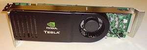
Nvidia Tesla
Nvidia Tesla is the name of Nvidia's line of products targeted at stream processing or general-purpose graphics processing units (GPGPU), named after pioneering electrical engineer Nikola Tesla. Its products began using GPUs from the G80 series, and have continued to accompany the release of new chips. They are programmable using the CUDA or OpenCL APIs.
 |
The Nvidia Tesla product line directly competes with AMD's Radeon Instinct and Intel Xeon Phi lines of deep learning and GPGPU cards.
Nvidia has retired the Tesla brand with the release of the Nvidia Ampere A100 GPU.[1]
Overview

Offering computational power much greater than traditional microprocessors, the Tesla products target the high-performance computing market.[2] As of 2012, Nvidia Teslas power some of the world's fastest supercomputers, including Summit at Oak Ridge National Laboratory and Tianhe-1A, in Tianjin, China.
Compared to GeForce cards, Tesla cards have four times the double precision performance of a Fermi-based Nvidia GeForce card of similar single precision performance. Contrarily to Nvidia's consumer level GeForce cards and the professional level Nvidia Quadro cards, Tesla cards were originally unable to output images to a display. However, the latest Tesla C-class products include one Dual-Link DVI port.[3]
As part of Project Denver, Nvidia intends to offer ARMv8 processor cores embedded into future Tesla GPUs.[4] This will be a 64-bit follow-up to the 32-bit Tegra chips.
The Tesla P100 uses TSMC's 16 nanometer FinFET semiconductor manufacturing process, which is more advanced than the 28 nanometer process previously used by AMD and Nvidia GPUs between 2012 and 2016. The P100 also uses Samsung's HBM2 memory.[5]
Applications
Tesla products are primarily used in simulations and in large scale calculations (especially floating-point calculations), and for high-end image generation for applications in professional and scientific fields.[6]
The defense industry currently accounts for less than a sixth of Tesla sales, but Sumit Gupta predicts further sales to the geospatial intelligence market.[7]
Specifications
| Model | Micro- architecture |
Launch | Chips | Core clock (MHz) |
Shaders | Memory | Processing power (GFLOPS)[lower-alpha 1] | CUDA compute ability[lower-alpha 2] |
TDP (watts) |
Notes, form_factor | ||||||||
|---|---|---|---|---|---|---|---|---|---|---|---|---|---|---|---|---|---|---|
| Cuda cores (total) |
Base clock (MHz) | Max boost clock (MHz)[lower-alpha 3] |
Bus type | Bus width (bit) |
Size (GB) |
Clock (MT/s) |
Bandwidth (GB/s) |
Single precision (MAD+MUL) |
Single precision (MAD or FMA) |
Double precision (FMA) | ||||||||
| Units | MHz | MHz | W | |||||||||||||||
| C870 GPU Computing Module[lower-alpha 4] | Tesla | May 2, 2007 | 1× G80 | 600 | 128 | 1350 | N/A | GDDR3 | 384 | 1.5 | 1600 | 76.8 | 518.4 | 345.6 | No | 1.0 | 170.9 | Internal PCIe GPU (full-height, dual-slot) |
| D870 Deskside Computer[lower-alpha 4] | May 2, 2007 | 2× G80 | 600 | 256 | 1350 | N/A | GDDR3 | 2× 384 | 2× 1.5 | 1600 | 2× 76.8 | 1036.8 | 691.2 | No | 1.0 | 520 | Deskside or 3U rack-mount external GPUs | |
| S870 GPU Computing Server[lower-alpha 4] | May 2, 2007 | 4× G80 | 600 | 512 | 1350 | N/A | GDDR3 | 4× 384 | 4× 1.5 | 1600 | 4× 76.8 | 2073.6 | 1382.4 | No | 1.0 | 1U rack-mount external GPUs, connect via 2× PCIe (×16) | ||
| C1060 GPU Computing Module[lower-alpha 5] | April 9, 2009 | 1× GT200 | 602 | 240 | 1296[9] | N/A | GDDR3 | 512 | 4 | 1600 | 102.4 | 933.12 | 622.08 | 77.76 | 1.3 | 187.8 | Internal PCIe GPU (full-height, dual-slot) | |
| S1070 GPU Computing Server "400 configuration"[lower-alpha 5] | June 1, 2008 | 4× GT200 | 602 | 960 | 1296 | N/A | GDDR3 | 4× 512 | 4× 4 | 1538.4 | 4× 98.5 | 3732.5 | 2488.3 | 311.0 | 1.3 | 800 | 1U rack-mount external GPUs, connect via 2× PCIe (×8 or ×16) | |
| S1070 GPU Computing Server "500 configuration"[lower-alpha 5] | 1440 | N/A | 4147.2 | 2764.8 | 345.6 | |||||||||||||
| S1075 GPU Computing Server[lower-alpha 5][10] | June 1, 2008 | 4× GT200 | 602 | 960 | 1440 | N/A | GDDR3 | 4× 512 | 4× 4 | 1538.4 | 4× 98.5 | 4147.2 | 2764.8 | 345.6 | 1.3 | 1U rack-mount external GPUs, connect via 1× PCIe (×8 or ×16) | ||
| Quadro Plex 2200 D2 Visual Computing System[lower-alpha 6] | 2× GT200GL | 648 | 480 | 1296 | N/A | GDDR3 | 2× 512 | 2× 4 | 1600 | 2× 102.4 | 1866.2 | 1244.2 | 155.5 | 1.3 | Deskside or 3U rack-mount external GPUs with 4 dual-link DVI outputs | |||
| Quadro Plex 2200 S4 Visual Computing System[lower-alpha 6] | 4× GT200GL | 648 | 960 | 1296 | N/A | GDDR3 | 4× 512 | 4× 4 | 1600 | 4× 102.4 | 3732.5 | 2488.3 | 311.0 | 1.3 | 1200 | 1U rack-mount external GPUs, connect via 2× PCIe (×8 or ×16) | ||
| C2050 GPU Computing Module[11] | Fermi | July 25, 2011 | 1× GF100 | 575 | 448 | 1150 | N/A | GDDR5 | 384 | 3[lower-alpha 7] | 3000 | 144 | No | 1030.4 | 515.2 | 2.0 | 247 | Internal PCIe GPU (full-height, dual-slot) |
| M2050 GPU Computing Module[12] | July 25, 2011 | N/A | 3092 | 148.4 | No | 225 | ||||||||||||
| C2070 GPU Computing Module[11] | July 25, 2011 | 1× GF100 | 575 | 448 | 1150 | N/A | GDDR5 | 384 | 6[lower-alpha 7] | 3000 | 144 | No | 1030.4 | 515.2 | 2.0 | 247 | Internal PCIe GPU (full-height, dual-slot) | |
| C2075 GPU Computing Module[13] | July 25, 2011 | N/A | 3000 | 144 | No | 225 | ||||||||||||
| M2070/M2070Q GPU Computing Module[14] | July 25, 2011 | N/A | 3132 | 150.336 | No | 225 | ||||||||||||
| M2090 GPU Computing Module[15] | July 25, 2011 | 1× GF110 | 650 | 512 | 1300 | N/A | GDDR5 | 384 | 6[lower-alpha 7] | 3700 | 177.6 | No | 1331.2 | 665.6 | 2.0 | 225 | Internal PCIe GPU (full-height, dual-slot) | |
| S2050 GPU Computing Server | July 25, 2011 | 4× GF100 | 575 | 1792 | 1150 | N/A | GDDR5 | 4× 384 | 4× 3[lower-alpha 7] | 3 | 4× 148.4 | No | 4121.6 | 2060.8 | 2.0 | 900 | 1U rack-mount external GPUs, connect via 2× PCIe (×8 or ×16) | |
| S2070 GPU Computing Server | N/A | 4× 6[lower-alpha 7] | No | |||||||||||||||
| K10 GPU accelerator[16] | Kepler | May 1, 2012 | 2× GK104 | N/A | 3072 | 745 | ? | GDDR5 | 2× 256 | 2× 4 | 5000 | 2× 160 | No | 4577 | 190.7 | 3.0 | 225 | Internal PCIe GPU (full-height, dual-slot) |
| K20 GPU accelerator[17][18] | November 12, 2012 | 1× GK110 | N/A | 2496 | 706 | 758 | GDDR5 | 320 | 5 | 5200 | 208 | No | 3524 | 1175 | 3.5 | 225 | Internal PCIe GPU (full-height, dual-slot) | |
| K20X GPU accelerator[19] | November 12, 2012 | 1× GK110 | N/A | 2688 | 732 | ? | GDDR5 | 384 | 6 | 5200 | 250 | No | 3935 | 1312 | 3.5 | 235 | Internal PCIe GPU (full-height, dual-slot) | |
| K40 GPU accelerator[20] | October 8, 2013 | 1× GK110B | N/A | 2880 | 745 | 875 | GDDR5 | 384 | 12[lower-alpha 7] | 6000 | 288 | No | 4291–5040 | 1430–1680 | 3.5 | 235 | Internal PCIe GPU (full-height, dual-slot) | |
| K80 GPU accelerator[21] | November 17, 2014 | 2× GK210 | N/A | 4992 | 560 | 875 | GDDR5 | 2× 384 | 2× 12 | 5000 | 2× 240 | No | 5591–8736 | 1864–2912 | 3.7 | 300 | Internal PCIe GPU (full-height, dual-slot) | |
| M4 GPU accelerator[22][23] | Maxwell | November 10, 2015 | 1× GM206 | N/A | 1024 | 872 | 1072 | GDDR5 | 128 | 4 | 5500 | 88 | No | 1786–2195 | 55.81–68.61 | 5.2 | 50–75 | Internal PCIe GPU (half-height, single-slot) |
| M6 GPU accelerator[24] | August 30, 2015 | 1× GM204 | N/A | 1536 | 722 | 1051 | GDDR5 | 256 | 8 | 4600 | 147.2 | No | 2218–3229 | 69.3–100.9 | 5.2 | 75–100 | Internal MXM GPU | |
| M10 GPU accelerator[25] | 4× GM107 | N/A | 2560 | 1033 | ? | GDDR5 | 4× 128 | 4× 8 | 5188 | 4× 83 | No | 5289 | 165.3 | 5.2 | 225 | Internal PCIe GPU (full-height, dual-slot) | ||
| M40 GPU accelerator[23][26] | November 10, 2015 | 1× GM200 | N/A | 3072 | 948 | 1114 | GDDR5 | 384 | 12 | 6000 | 288 | No | 5825–6844 | 182.0–213.9 | 5.2 | 250 | Internal PCIe GPU (full-height, dual-slot) | |
| M60 GPU accelerator[27] | August 30, 2015 | 2× GM204 | N/A | 4096 | 899 | 1178 | GDDR5 | 2× 256 | 2× 8 | 5000 | 2× 160 | No | 7365–9650 | 230.1–301.6 | 5.2 | 225–300 | Internal PCIe GPU (full-height, dual-slot) | |
| P4 GPU accelerator[28] | Pascal | September 13, 2016 | 1× GP104 | N/A | 2560 | 810 | 1063 | GDDR5 | 256 | 8 | 6000 | 192.0 | No | 4147–5443 | 129.6–170.1 | 6.1 | 50-75 | PCIe card |
| P6 GPU accelerator[29][30] | March 24, 2017 | 1× GP104-995 | N/A | 2048 | 1012 | 1506 | GDDR5 | 256 | 16 | 3003 | 192.2 | No | 6169 | 192.8 | 6.1 | 90 | MXM card | |
| P40 GPU accelerator[28] | September 13, 2016 | 1× GP102 | N/A | 3840 | 1303 | 1531 | GDDR5 | 384 | 24 | 7200 | 345.6 | No | 10007–11758 | 312.7–367.4 | 6.1 | 250 | PCIe card | |
| P100 GPU accelerator (mezzanine)[31][32] | April 5, 2016 | 1× GP100 | N/A | 3584 | 1328 | 1480 | HBM2 | 4096 | 16 | 1430 | 732 | No | 9519–10609 | 4760–5304 | 6.0 | 300 | NVLink card | |
| P100 GPU accelerator (16 GB card)[33] | June 20, 2016 | N/A | 1126 | 1303 | No | 8071‒9340 | 4036‒4670 | 250 | PCIe card | |||||||||
| P100 GPU accelerator (12 GB card)[33] | June 20, 2016 | N/A | 3072 | 12 | 549 | No | 8071‒9340 | 4036‒4670 | ||||||||||
| V100 GPU accelerator (mezzanine)[34][35][36] | Volta | 1× GV100 | N/A | 5120 | Unknown | 1455 | HBM2 | 4096 | 16 or 32 | 1750 | 900 | No | 14899 | 7450 | 7.0 | 300 | NVlink card | |
| V100 GPU accelerator (PCIe card)[34][35][36] | June 21, 2017 | N/A | Unknown | 1370 | No | 14028 | 7014 | 250 | PCIe card | |||||||||
| T4 GPU accelerator (PCIe card)[37][38] | Turing | September 12, 2018 | 1× TU104 | N/A | 2560 | 585 | 1590 | GDDR6 | 256 | 16 | Unknown | 320 | No | 8100 | Unknown | 7.5 | 70 | PCIe card |
| Model | Micro- architecture |
Launch | Chips | Core clock (MHz) |
Shaders | Memory | Processing power (GFLOPS)[lower-alpha 1] | CUDA compute ability |
TDP (watts) |
Notes, form factor | ||||||||
| Cuda cores (total) |
Base clock (MHz) | Max boost clock (MHz)[lower-alpha 3] |
Bus type | Bus width (bit) |
Size (GB) |
Clock (MT/s) |
Bandwidth (total) (GB/s) |
Single precision (MAD+MUL) |
Single precision (MAD or FMA) |
Double precision (FMA) | ||||||||
Notes
- To calculate the processing power see Tesla (microarchitecture)#Performance, Fermi (microarchitecture)#Performance, Kepler (microarchitecture)#Performance, Maxwell (microarchitecture)#Performance, or Pascal (microarchitecture)#Performance. A number range specifies the minimum and maximum processing power at, respectively, the base clock and maximum boost clock.
- Core architecture version according to the CUDA programming guide.
- GPU Boost is a default feature that increases the core clock rate while remaining under the card's predetermined power budget. Multiple boost clocks are available, but this table lists the highest clock supported by each card.[8]
- Specifications not specified by Nvidia assumed to be based on the GeForce 8800GTX
- Specifications not specified by Nvidia assumed to be based on the GeForce GTX 280
- Specifications not specified by Nvidia assumed to be based on the Quadro FX 5800
- With ECC on, a portion of the dedicated memory is used for ECC bits, so the available user memory is reduced by 12.5%. (e.g. 4 GB total memory yields 3.5 GB of user available memory.)
See also
References
- https://www.nvidia.com/en-us/data-center/a100/
- "High Performance Computing - Supercomputing with Tesla GPUs".
- "Professional Workstation Solutions".
- "Nvidia to Integrate ARM Processors in Tesla". 1 November 2012.
- Walton, Mark (6 April 2016). "Nvidia unveils first Pascal graphics card, the monstrous Tesla P100". Ars Technica. Retrieved 19 June 2019.
- Tesla Technical Brief (PDF)
- "Nvidia chases defense, intelligence ISVs with GPUs."
- "Nvidia GPU Boost For Tesla" (PDF). January 2014. Retrieved 7 December 2015.
- "Tesla C1060 Computing Processor Board" (PDF). Nvidia.com. Retrieved 11 December 2015.
- "Difference between Tesla S1070 and S1075". 31 October 2008. Retrieved 29 January 2017.
S1075 has one interface card
- "Tesla C2050 and Tesla C2070 Computing Processor" (PDF). Nvidia.com. Retrieved 11 December 2015.
- "Tesla M2050 and Tesla M2070/M2070Q Dual-Slot Computing Processor Modules" (PDF). Nvidia.com. Retrieved 11 December 2015.
- "Tesla C2075 Computing Processor Board" (PDF). Nvidia.com. Retrieved 11 December 2015.
- Hand, Randall (23 August 2010). "NVidia Tesla M2050 & M2070/M2070Q Specs OnlineVizWorld.com". VizWorld.com. Retrieved 11 December 2015.
- "Tesla M2090 Dual-Slot Computing Processor Module" (PDF). Nvidia.com. Retrieved 11 December 2015.
- "Tesla K10 GPU accelerator" (PDF). Nvidia.com. Retrieved 11 December 2015.
- "Tesla K20 GPU active accelerator" (PDF). Nvidia.com. Retrieved 11 December 2015.
- "Tesla K20 GPU accelerator" (PDF). Nvidia.com. Retrieved 11 December 2015.
- "Tesla K20X GPU accelerator" (PDF). Nvidia.com. Retrieved 11 December 2015.
- "Tesla K40 GPU accelerator" (PDF). Nvidia.com. Retrieved 11 December 2015.
- "Tesla K80 GPU accelerator" (PDF). Images.nvidia.com. Retrieved 11 December 2015.
- "Nvidia Announces Tesla M40 & M4 Server Cards - Data Center Machine Learning". Anandtech.com. Retrieved 11 December 2015.
- "Accelerating Hyperscale Datacenter Applications with Tesla GPUs | Parallel Forall". Devblogs.nvidia.com. 10 November 2015. Retrieved 11 December 2015.
- "Tesla M6" (PDF). Images.nvidia.com. Retrieved 28 May 2016.
- "Tesla M10" (PDF). Images.nvidia.com. Retrieved 29 October 2016.
- "Tesla M40" (PDF). Images.nvidia.com. Retrieved 11 December 2015.
- "Tesla M60" (PDF). Images.nvidia.com. Retrieved 27 May 2016.
- Smith, Ryan (13 September 2016). "Nvidia Announces Tesla P40 & Tesla P4 - Network Inference, Big & Small". Anandtech. Retrieved 13 September 2016.
- "Tesla P6" (PDF). www.nvidia.com. Retrieved 7 March 2019.
- "Tesla P6 Specs". www.techpowerup.com. Retrieved 7 March 2019.
- Smith, Ryan (5 April 2016). "Nvidia Announces Tesla P100 Accelerator - Pascal GP100 for HPC". Anandtech.com. Anandtech.com. Retrieved 5 April 2016.
- Harris, Mark. "Inside Pascal: Nvidia's Newest Computing Platform". Retrieved 13 September 2016.
- Smith, Ryan (20 June 2016). "NVidia Announces PCI Express Tesla P100". Anandtech.com. Retrieved 21 June 2016.
- Smith, Ryan (10 May 2017). "The Nvidia GPU Technology Conference 2017 Keynote Live Blog". Anandtech. Retrieved 10 May 2017.
- Smith, Ryan (10 May 2017). "NVIDIA Volta Unveiled: GV100 GPU and Tesla V100 Accelerator Announced". Anandtech. Retrieved 10 May 2017.
- Oh, Nate (20 June 2017). "NVIDIA Formally Announces V100: Available later this Year". Anandtech.com. Retrieved 20 June 2017.
- "NVIDIA TESLA T4 TENSOR CORE GPU". NVIDIA. Retrieved 17 October 2018.
- "NVIDIA Tesla T4 Tensor Core Product Brief" (PDF). www.nvidia.com. Retrieved 10 July 2019.
External links
| Wikimedia Commons has media related to Nvidia Tesla series. |