Extreme ultraviolet lithography
Extreme ultraviolet lithography (also known as EUV or EUVL) is a lithography technology using a range of extreme ultraviolet (EUV) wavelengths, roughly spanning a 2% FWHM bandwidth about 13.5 nm.
.svg.png)
While EUV technology is available for mass production, fewer than fifty machines worldwide are capable of producing wafers using the technique;[1] by comparison, as of 2013, over 200 Deep Ultraviolet Lithography (DUV) immersion systems were already deployed.[2] As of Q3 2019, 5.7 million wafers have been exposed on EUV production tools; 1.7 million wafers were exposed in Q1-Q3 alone, while the number of tools increased from 31 to 45 (on the order of 10 WPH per tool).[3] Issues that make EUV adoption difficult are tool costs (ASML's EUV scanners can cost up to US$120 Million[4][5]), tool uptime and stochastic phenomena.[6]
Masks
EUV photomasks work by reflecting light,[7] which is achieved by using multiple alternating layers of molybdenum and silicon. An EUV mask consists of 40 alternating silicon and molybdenum layers;[8] this multilayer acts to reflect the extreme ultraviolet light through Bragg diffraction; the reflectance is a strong function of incident angle and wavelength, with longer wavelengths reflecting more near normal incidence and shorter wavelengths reflecting more away from normal incidence. The pattern is defined in a tantalum-based absorbing layer over the multilayer.[9]
Manufacturing
Blank photomasks are mainly made by two companies: AGC Inc. and Hoya Corporation.[10][11] A blank photomask is covered with photoresist, which is then exposed using a laser, using maskless lithography.[12] The exposed photoresist is developed (removed) and the unprotected areas are etched. The remaining photoresist is then removed. Masks are then inspected and later repaired using an electron beam.[13] Etching must be done to a very specific depth thus making etching difficult when compared with conventional photomask manufacturing.[14]
Tool
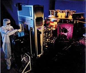
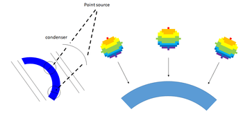
The tool consists of a laser-driven tin (Sn) plasma light source, reflective optics comprising multilayer mirrors, contained within a hydrogen gas ambient. The hydrogen is used for keeping the EUV collector mirror in the source free of Sn deposition.[15]
EUVL is a significant departure from the deep ultraviolet lithography standard. All matter absorbs EUV radiation. Hence, EUV lithography requires a vacuum. All optical elements, including the photomask, must use defect-free molybdenum/silicon (Mo/Si) multilayers (consisting of 40 Mo/Si bilayers) that act to reflect light by means of interlayer interference; any one of these mirrors absorb around 30% of the incident light.
Current EUVL systems contain at least two condenser multilayer mirrors, six projection multilayer mirrors and a multilayer object (mask). Since the mirrors absorb 96% of the EUV light, the ideal EUV source needs to be much brighter than its predecessors. EUV source development has focused on plasmas generated by laser or discharge pulses. The mirror responsible for collecting the light is directly exposed to the plasma and is vulnerable to damage from high-energy ions[16][17] and other debris.[18]
Resource requirements
| Utility | 200 W output EUV | 90 W output ArF immersion double patterning |
|---|---|---|
| Electrical power (kW) | 532 | 49 |
| Cooling water flow (L/min) | 1600 | 75 |
| Gas lines | 6 | 3 |
Source: Gigaphoton, Sematech Symposium Japan, September 15, 2010
The required utility resources are significantly larger for EUV compared to 193 nm immersion, even with two exposures using the latter. Hynix reported at the 2009 EUV Symposium that the wall plug efficiency was ~0.02% for EUV, i.e., to get 200-watts at intermediate focus for 100 wafers-per-hour, one would require 1-megawatt of input power, compared to 165-kilowatts for an ArF immersion scanner, and that even at the same throughput, the footprint of the EUV scanner was ~3x the footprint of an ArF immersion scanner, resulting in productivity loss.[19] Additionally, to confine ion debris, a superconducting magnet may be required.[20]
A typical EUV tool weighs 180 tons.[21]
Summary of key features
The following table summarizes key differences between EUV systems in development and ArF immersion systems which are widely used in production today:
| EUV | ArF immersion | |
|---|---|---|
| Wavelength | 2% FWHM bandwidth about 13.5 nm | 193 nm |
| Photon energy | 91-93 eV | 6.4 eV |
| Light source | CO2 laser + Sn plasma | ArF excimer laser |
| Wavelength bandwidth | 5.9%[22] | <0.16%[23] |
| Secondary electrons produced by absorption | Yes | No |
| Optics | Reflective multilayers (~40% absorbing per mirror) | Transmissive lenses |
| Numerical aperture (NA) | 0.25: NXE:3100 0.33: NXE:33x0 and NXE:3400B High NA (0.55): in development |
1.2, 1.35 |
| Resolution spec Note: k1 defined here as resolution/(wavelength/numerical aperture) |
NXE:3100: 27 nm (k1=0.5) NXE:3300B: 22 nm (k1=0.54), 18 nm (k1=0.44) with off-axis illumination NXE:3350B: 16 nm (k1=0.39) NXE:3400B: 13 nm (k1=0.32) |
38 nm (k1=0.27) |
| Flare | 4%[24] | <1%[25] |
| Illumination | Central angle 6 degrees off axis onto reticle | On axis |
| Field size | 0.25 and 0.33 NA: 26 mm X 33 mm High NA: 26 mm X 16.5 mm[26] |
26 mm X 33 mm |
| Magnification | 0.25 and 0.33 NA: 4X isomorphic High NA: 4X/8X anamorphic |
4X |
| Ambient | Vacuum hydrogen | Air (exposed wafer area underwater) |
| Aberration control (including thermal) | None | Yes, e.g., FlexWave[27] |
| Illumination slit | Arc-shaped[28] | Rectangular[29] |
| Reticle | Pattern on reflective multilayer | Pattern on transmissive substrate |
| Wafer pattern shift with reticle vertical position | Yes (due to reflection); ~1:40[30] | No |
| Pellicle | Available, but has issues | Yes |
| Wafers per day (Note: depends on tool and dose) | 1000 | 6000 |
| # tools in field | 36 (all 0.33 NA tool models) | > 400 |
The different degrees of resolution among the 0.33 NA tools are due to the different illumination options. Despite the potential of the optics to reach sub-20 nm resolution, secondary electrons in resist practically limit the resolution to around 20 nm.[31]
Light source power, throughput, and uptime
.png)
Neutral atoms or condensed matter cannot emit EUV radiation. Ionization must precede EUV emission in matter. The thermal production of multicharged positive ions is only possible in a hot dense plasma, which itself strongly absorbs EUV.[32] As of 2016, the established EUV light source is a laser-pulsed tin plasma.[33] The ions absorb the EUV light they emit, and are easily neutralized by electrons in the plasma to lower charge states which produce light mainly at other, unusable wavelengths, which results in a much reduced efficiency of light generation for lithography at higher plasma power density.
The throughput is tied to the source power, divided by the dose.[34] A higher dose requires a slower stage motion (lower throughput) if pulse power cannot be increased.
EUV collector reflectivity degrades ~0.1-0.3% per billion 50kHz pulses (~10% in ~2 weeks), leading to loss of uptime and throughput, while even for the first few billion pulses (within one day), there is still 20% (+/-10%) fluctuation.[35] This could be due to the accumulating Sn residue mentioned above which is not completely cleaned off.[36][37] On the other hand, conventional immersion lithography tools for double patterning provide consistent output for up to a year.[38]
Recently, the NXE:3400B illuminator features a smaller pupil fill ratio (PFR) down to 20% without transmission loss.[39] PFR is maximized and greater than 0.2 around a metal pitch of 45 nm.[40]
Due to the use of EUV mirrors which also absorb EUV light, only a small fraction of the source light is finally available at the wafer. There are 4 mirrors used for the illumination optics, and 6 mirrors for the projection optics. The EUV mask or reticle is itself an additional mirror. With 11 reflections, only ~ 2% of the EUV source light is available at the wafer.[41]
A further complication for EUV tool throughput is the ring shape of the exposure slit, in contrast to the conventional rectangular shape.[42] Consequently, slit width and height are effectively confounded in a complicated fashion.
Tool uptime
The EUV light source limits tool uptime besides throughput. In a two-week period, for example, over seven hours downtime may be scheduled, while total actual downtime including unscheduled issues could easily exceed a day.[41] A dose error over 2% warrants tool downtime.[41]
Comparison to other lithography light sources
While state-of-the-art 193 nm ArF excimer lasers offer intensities of 200 W/cm2,[43] lasers for producing EUV-generating plasmas need to be much more intense, on the order of 1011 W/cm2.[44] A state-of-the-art ArF immersion lithography 120 W light source requires no more than 40 kW[45] while EUV sources are targeted to exceed 40 kW.[46]
The power target for EUV lithography is at least 250 W, while for other conventional lithography sources, it is much less.[41] For example, immersion lithography light sources target 90 W, dry ArF sources 45 W, and KrF sources 40 W. High-NA EUV sources are expected to require at least 500 W.[41]
EUV stochastic issues


EUV lithography is particularly sensitive to stochastic effects.[47] In a large population of features printed by EUV, although the overwhelming majority are resolved, some suffer complete failure to print, e.g. missing holes or bridging lines. A known significant contribution to this effect is the dose used to print.[48] This is related to shot noise , to be discussed further below. Due to the stochastic variations in arriving photon numbers, some areas designated to print actually fail to reach the threshold to print, leaving unexposed defect regions. Some areas may be overexposed, leading to excessive resist loss or crosslinking. The probability of stochastic failure increases exponentially as feature size decreases, and for the same feature size, increasing distance between features also significantly increases the probability.[48] Line cuts which are relatively widely spaced are a significant issue. Yield requires detection of stochastic failures down to below 1e-12.[48]
The tendency to stochastic defects is worse when the image consists of photons from different patterns, such as from a large-area pattern[49] or from defocus over a large pupil fill.[50][51]
Multiple failure modes may exist for the same population. For example, besides bridging of trenches, the lines separating the trenches may be broken.[48] This can be attributed to stochastic resist loss,[47] from secondary electrons.[52][53]
The coexistence of stochastically underexposed and overexposed defect regions leads to a loss of dose window at a certain post-etch defect level between the low-dose and high-dose patterning cliffs.[54] Hence, the resolution benefit from shorter wavelength is lost.
The resist underlayer also plays an important role.[48] This could be due to the secondary electrons generated by the underlayer.[55] Secondary electrons may remove over 10 nm of resist from the exposed edge.[52][56]
The defect level is on the order of 1K/mm2.[57]

Photon shot noise can be linked to stochastic defects through the presence of dose-dependent blur (modeled as Gaussian).[58]
EUV-specific optical issues
Multilayer reflectivity random variations
GlobalFoundries and Lawrence Berkeley Labs carried out a Monte Carlo study to simulate the effects of intermixing between the molybdenum (Mo) and silicon (Si) layes in the multilayer that is used to reflect EUV light from the EUV mask.[59] The results indicated high sensitivity to the atomic-scale variations of layer thickness. Such variations could not be detected by wide-area reflectivity measurements, but would be significant on the scale of the critical dimension (CD).[59]
Wavelength bandwidth (chromatic aberration)
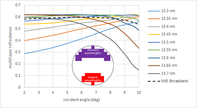
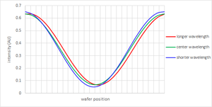
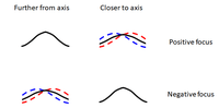
Unlike DUV lithography sources, based on excimer lasers, EUV plasma sources produce light across a broad range of wavelengths.[61] Though the EUV spectrum is not completely monochromatic, nor even as spectrally pure as DUV laser sources, the working wavelength has generally been taken to be 13.5 nm. In actuality, the reflected power is distributed mostly in the 13.3-13.7 nm range.[62] The bandwidth of EUV light reflected by a multilayer mirror used for EUV lithography is over +/-2% (>270 pm);[63] the phase changes due to wavelength changes at a given illumination angle may be calculated[64] and compared to the aberration budget.[65] Wavelength dependence of reflectance[64][62] also affects the apodization, or illumination distribution across the pupil (for different angles); different wavelengths effectively 'see' different illuminations as they are reflected differently by the multilayer of the mask.[66][62] This effective source illumination tilt can lead to large image shifts due to defocus.[67] Conversely, the peak reflected wavelength varies across the pupil due to different incident angles.[62][68] This is aggravated when the angles span a wide radius, e.g., annular illumination. The peak reflectance wavelength increases for smaller incident angles.[69] Aperiodic multilayers have been proposed to reduce the sensitivity at the cost of lower reflectivity but are too sensitive to random fluctuations of layer thicknesses, such as from thickness control imprecision or interdiffusion.[70] In particular, defocused dense lines at pitches up to twice the minimum resolvable pitch suffer wavelength-dependent edge shifts.[71]
A narrower bandwidth would increase sensitivity to mask absorber and buffer thickness on the 1 nm scale.[72][73]
Mask absorber phase effects

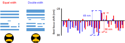
The EUV mask absorber, due to partial transmission, generates a phase difference between the 0th and 1st diffraction orders of a line-space pattern, resulting in image shifts (at a given illumination angle) as well as changes in peak intensity (leading to linewidth changes)[74] which are further enhanced due to defocus.[75][76] Ultimately, this results in different positions of best focus for different pitches and different illumination angles. Generally, the image shift is balanced out due to illumination source points being paired (each on opposite sides of the optical axis). However, the separate images are superposed and the resulting image contrast is degraded when the individual source image shifts are large enough. The phase difference ultimately also determines the best focus position.
Reflective optics

A fundamental aspect of EUVL tools, resulting from the use of reflective optics, is the off-axis illumination (at an angle of 6 degrees, in different direction at different positions within the illumination slit)[77] on a multilayer mask. This leads to shadowing effects resulting in asymmetry in the diffraction pattern that degrade pattern fidelity in various ways as described below.[78]
Thick mask shadowing effects
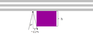
The oblique incidence in a reflective optical system leads to shadowing effects in the presence of a mask absorber. For example, one side (behind the shadow) would appear brighter than the other (within the shadow).[79]
H-V asymmetry

Most fundamentally, the behavior of light rays within the plane of reflection (affecting horizontal lines) is different from the behavior of light rays out of the plane of reflection (affecting vertical lines).[80] Most conspicuously, identically sized horizontal and vertical lines on the EUV mask are printed at different sizes on the wafer.

Asymmetries in sets of parallel lines
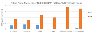
The combination of the off-axis asymmetry and the mask shadowing effect leads to a fundamental inability of two identical features even in close proximity to be in focus simultaneously.[81] One of EUVL's key issues is the asymmetry between the top and bottom line of a pair of horizontal lines (the so-called "two-bar"). Some ways to partly compensate are the use of assist features as well as asymmetric illumination.[82]
An extension of the two-bar case to a grating consisting of many horizontal lines shows similar sensitivity to defocus.[83] It is manifest in the CD difference between the top and bottom edge lines of the set of 11 horizontal lines. The table below lists the CD difference over 100 nm focus range under quasar illumination (quasar illumination will be described in the section on optimum illumination vs. pitch).
| Pitch | Horizontal 11-bar bottom-top CD difference over 100 nm focus range (quasar) |
|---|---|
| 36 nm | 3.5 nm |
| 40 nm | 2.5 nm |
| 44 nm | 1.7 nm |
For pitches of 40 nm or below, the linewidths are 20 nm or less, while the CD difference is at least 2.5 nm, resulting in at least 12.5% difference.

Pattern shift from defocus (non-telecentricity)
Mask feature vertical placement
The use of reflection causes wafer exposure position to be extremely sensitive to the reticle flatness and the reticle clamp. Reticle clamp cleanliness is therefore required to be maintained. Small (mrad-scale) deviations in mask flatness in the local slope, coupled with wafer defocus.[84] More significantly, mask defocus has been found to result in large overlay errors.[85][86] In particular, for a 10 nm node metal 1 layer (including 48 nm, 64 nm, 70 nm pitches, isolated, and power lines), the uncorrectable pattern placement error was 1 nm for 40 nm mask z-position shift.[87] This is a global pattern shift of the layer with respect to previously defined layers. However, features at different locations will also shift differently due to different local deviations from mask flatness, e.g., from defects buried under the multilayer. It can be estimated that the contribution of mask non-flatness to overlay error is roughly 1/40 times the peak-to-valley thickness variation.[88] With the blank peak-to-valley spec of 50 nm, ~1.25 nm image placement error is possible. Blank thickness variations up to 80 nm also contribute, which lead to up to 2 nm image shift.[88]
Wafer defocus
The off-axis illumination of the reticle is also the cause of non-telecentricity in wafer defocus, which consumes most of the 1.4 nm overlay budget of the NXE:3400 EUV scanner[89] even for design rules as loose as 100 nm pitch.[90] The worst uncorrectable pattern placement error for a 24 nm line was about 1.1 nm, relative to an adjacent 72 nm power line, per 80 nm wafer focus position shift at a single slit position; when across-slit performance is included, the worst error is over 1.5 nm in the wafer defocus window[87] In 2017, an actinic microscope mimicking a 0.33 NA EUV lithography system with 0.2/0.9 quasar 45 illumination showed that an 80 nm pitch contact array shifted -0.6 to 1.0 nm while a 56 nm pitch contact array shifted -1.7 to 1.0 nm relative to a horizontal reference line, within a +/- 50 nm defocus window.[91]
Wafer defocus also leads to image placement errors due to deviations from local mask flatness. If the local slope is indicated by an angle α, the image is projected to be shifted in a 4x projection tool by 8 α x (DOF/2) = 4 α DOF, where DOF is the depth of focus.[92] For a depth of focus of 100 nm, a small local deviation from flatness of 2.5 mrad (0.14°) can lead to a pattern shift of 1 nm.
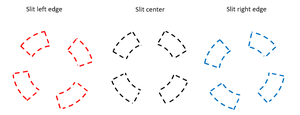
Slit position dependence
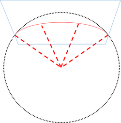
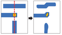
The direction of illumination is also highly dependent on slit position, essentially rotated azimuthally.[96][97][28][98][99][100] The reason for this is a mirror is used to transform straight rectangular fields into arc-shaped fields.[101][102] More generally, so-called "ring-field" systems reduce aberrations by relying on the radial symmetry of an arc-shaped field derived from an off-axis annulus.[103] This is preferred, as reflective systems must use off-axis paths, which aggravate aberrations. Hence identical die patterns within different halves of the arc-shaped slit would require different OPC. This renders them uninspectable by die-to-die comparison, as they are no longer truly identical dies. For pitches requiring dipole, quadrupole, or hexapole illumination, the rotation also causes mismatch with the same pattern layout at a different slit position, i.e., edge vs. center. Even with annular or circular illumination, the rotational symmetry is destroyed by the angle-dependent multilayer reflectance described above. Although the azimuthal angle range is +/- ~20° on 0.33 NA scanners,[28][98][104][105] at 7nm design rules (36-40 nm pitch), the tolerance for (quasar) illumination can be +/-15°,[106][107] or even less.[108][109] Annular illumination nonuniformity and asymmetry also significantly impact the imaging.[110]
The slit position dependence is particularly difficult for the tilted patterns encountered in DRAM.[99] Besides the more complicated effects due to shadowing and pupil rotation, tilted edges are converted to stair shape, which may be distorted by OPC.

Aberrations, originating from deviations of optical surfaces from subatomic (<0.1 nm) specifications[111] as well as thermal deformations[112][113] and possibly including polarized reflectance effects,[114] are also dependent on slit position,[115][113] as will be further discussed below, with regard to source-mask optimization (SMO). The thermally induced aberrations are expected to exhibit differences among different positions across the slit, corresponding to different field positions, as each position encounters different parts of the deformed mirrors.[116] Ironically, the use of substrate materials with high thermal and mechanical stability make it more difficult to compensate wavefront errors[117]
Flare
Flare is the presence of background light originating from scattering off of surface features which are not resolved by the light. In EUV systems, this light can be EUV or out-of-band (OoB) light that is also produced by the EUV source. The OoB light adds the complication of affecting the resist exposure in ways other than accounted for by the EUV exposure. OoB light exposure may be alleviated by a layer coated above the resist, as well as 'black border' features on the EUV mask.[118] However, the layer coating inevitably absorbs EUV light, and the black border adds EUV mask processing cost.
Line tip effects


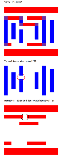
A key challenge for EUV is the counter-scaling behavior of the line tip-to-tip (T2T) distance as half-pitch (hp) is scaled down.[108] This is in part due to lower image contrast for the binary masks used in EUV lithography, which is not encountered with the use of phase shift masks in immersion lithography.[119][120] The rounding of the corners of the line end leads to line end shortening,[121] and this is worse for binary masks.[122] The use of phase-shift masks in EUV lithography has been studied but encounters difficulties from phase control in thin layers[123] as well as the bandwidth of the EUV light itself.[124] More conventionally, optical proximity correction (OPC) is used to address the corner rounding and line-end shortening. In spite of this, it has been shown that the tip-to-tip resolution and the line tip printability are traded off against each other, being effectively CDs of opposite polarity.[125] In addition, the effectiveness of optical corrections depends on other non-optical causes such as resist blur and diffusion effects, which may also include secondary electron blur (discussed in the section on photoresist exposure).[126] Also, larger molecular weights and sizes appear to reduce corner rounding.[127]
In unidirectional metal layers, tip-to-tip spacing is one of the more severe issues for single exposure patterning. For the 40 nm pitch vertical lines, an 18 nm nominal tip-to-tip drawn gap resulted in an actual tip-to-tip distance of 29 nm with OPC (optical proximity correction),[108] while for 32 nm pitch horizontal lines, the tip-to-tip distance with a 14 nm nominal gap went to 31 nm with OPC.[128] These actual tip-to-tip distances define a lower limit of the half-pitch of the metal running in the direction perpendicular to the tip. In this case, the lower limit is around 30 nm. With further optimization of the illumination (discussed in the section on source-mask optimization), the lower limit can be further reduced to around 25 nm.[129]
For larger pitches, where conventional illumination can be used, the line tip-to-tip distance is generally larger. For the 24 nm half-pitch lines, with a 20 nm nominally drawn gap, the distance was actually 45 nm, while for 32 nm half-pitch lines, the same nominal gap resulted in a tip-to-tip distance of 34 nm.[128] With OPC, these become 39 nm and 28 nm for 24 nm half-pitch and 32 nm half-pitch, respectively.[130]
The printed space between a line tip and a perpendicular line it faces is 25-35 nm for 22 nm half-pitch lines (with a 20 nm nominally drawn gap).[130] For a 22 nm line-space pattern with 22 nm nominal gap, conventional illumination yields a 38 nm tip-to-line distance, while quasar illumination yields a 28 nm distance.[131] The tip-to-side gap is one of the hardest features to print in a bidirectional pattern.[130]
Summary of EUV line tip and corner effects:[132]
| Corner rounding | Tip to tip | Tip to side |
|---|---|---|
| ~25 nm | 28 nm | 28 nm |
Source: Semicon West 2017, IBM
The line end clearance distance of 28 nm essentially forces pitches to be at least 56 nm for EUV single exposure bi-directional patterning. 7 nm node minimum metal pitch is already at 40 nm or below, while gate pitch can also be below 56 nm,[133][134] so this is an indication that multiple patterning would be needed even for EUV at 7 nm.[135]
Enhancement opportunities for EUV patterning
Assist features

Assist features are often used to help balance asymmetry from non-telecentricity at different slit positions, due to different illumination angles, starting at the 7 nm node,[136][137] where the pitch is ~ 41 nm for a wavelength ~13.5 nm and NA=0.33, corresponding to k1 ~ 0.5.[138] However, the asymmetry is reduced but not completely eliminated, since the assist features mainly enhance the highest spatial frequencies, whereas intermediate spatial frequencies, which also affect feature focus and position, are not much affected. The coupling between the primary image and the self images is too strong for the asymmetry to be completely eliminated by assist features; only asymmetric illumination can achieve this.[82] Assist features may also get in the way of access to power/ground rails. Power rails are expected to be wider, which also limits the effectiveness of using assist features, by constraining the local pitch. Local pitches between 1x and 2x the minimum pitch forbid assist feature placement, as there is simply no room to preserve the local pitch symmetry. In fact, for the application to the two-bar asymmetry case, the optimum assist feature placement may be less than or exceed the two-bar pitch.[137] Depending on the parameter to be optimized (process window area, depth of focus, exposure latitude), the optimum assist feature configuration can be very different, e.g., pitch between assist feature and bar being different from two-bar pitch, symmetric or asymmetric, etc..
At pitches smaller than 58 nm, there is a tradeoff between depth of focus enhancement and contrast loss by assist feature placement.[137] Generally, there is still a focus-exposure tradeoff as the dose window is constrained by the need to have the assist features not print accidentally.
An additional concern comes from shot noise;[139] sub-resolution assist features (SRAFs) cause the required dose to be lower, so as not to print the assist features accidentally.[140] This results in fewer photons defining smaller features (see discussion in section on shot noise).
It is now known that the underlying mechanism for the asymmetry is different shadowing from different angles of incidence. Hence, reducing absorber thickness would be the most direct way to resolve the issue.[141]
Stochastic printing of SRAFs

As SRAFs are smaller features than primary features and are not supposed to receive doses high enough to print, they are more susceptible to stochastic dose variations causing printing errors.[142] This is particularly prohibitive for EUV, where even when the primary feature is printed at 80 mJ/cm2, the SRAF suffers from stochastic printing.
Source-mask optimization

Due to the effects of non-telecentricity, standard illumination pupil shapes, such as disc or annular, are not sufficient to be used for feature sizes of ~20 nm or below (10 nm node and beyond).[90] Instead certain parts of the pupil (often over 50%) must be asymmetrically excluded. The parts to be excluded depend on the pattern. In particular, the densest allowed lines need to be aligned along one direction and prefer a dipole shape. For this situation, double exposure lithography would be required for 2D patterns, due to the presence of both X- and Y-oriented patterns, each requiring its own 1D pattern mask and dipole orientation.[143][144] There may be 200–400 illuminating points, each contributing its weight of the dose to balance the overall image through focus. Thus the shot noise effect (to be discussed later) critically affects the image position through focus, in a large population of features.
Double or multiple patterning would also be required if a pattern consists of sub-patterns which require significantly different optimized illuminations, due to different pitches, orientations, shapes, and sizes.
Impact of slit position and aberrations
Largely due to the slit shape,[104] and the presence of residual aberrations,[145] the effectiveness of SMO varies across slit position.[146] At each slit position, there are different aberrations[115] and different azimuthal angles of incidence leading to different shadowing.[28] Consequently, there could be uncorrected variations across slit for aberration-sensitive features, which may not be obviously seen with regular line-space patterns.[137] At each slit position, although optical proximity correction (OPC), including the assist features mentioned above, may also be applied to address the aberrations,[147][148] they also feedback into the illumination specification,[149][146][150][151] since the benefits differ for different illumination conditions.[147] This would necessitate the use of different source-mask combinations at each slit position, i.e., multiple mask exposures per layer.[115]
The above-mentioned chromatic aberrations, due to mask-induced apodization,[66] also lead to inconsistent source-mask optimizations for different wavelengths.
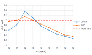
Optimum illumination vs. pitch

The optimum illumination, taking into account both exposure dose and focus windows, is a strong function of pitch in the range between 32 nm and 48 nm (relevant to 7 nm and 10 nm foundry nodes), which is where most of the work on EUV application has been focused. For pitches larger than 44 nm, the illumination pupil shape is preferably conventional, which is a circular disc, possibly including a central obscuration to provide an annular appearance.[128] For pitches in the range 44 nm down to 34 nm, the optimum shape is no longer conventional or annular but more shaped like the "quasar" (Quadrupole-shaped annular)[152] source, i.e., an arc within each quadrant of the pupil.[128] For pitches of 32 nm and below, the optimum illumination becomes more dipole like, i.e., concentrated toward the top and bottom or the left and right ends of the pupil.[108] When source-mask optimization is performed, the resulting shape will resemble the closest of the standard set (conventional, annular, quasar, dipole). For pitches less than 41 nm, the central portion of the pupil must be excluded for a tool with NA=0.33, as 13.5 nm EUV light going through that portion would only contribute the zeroth diffraction order (unscattered light), effectively adding flare.[153]
| Pitch | Standard illumination shape closest to optimum |
|---|---|
| 48 nm | Conventional/annular |
| 44 nm | Quasar or conventional/annular |
| 40 nm | Quasar |
| 36 nm | Quasar |
| 32 nm | Dipole |
| 28 nm | Dipole |
Pitch-dependent focus windows
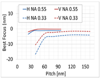
The best focus for a given feature size varies as a strong function of pitch, polarity, and orientation under a given illumination.[154] At 36 nm pitch, horizontal and vertical darkfield features have more than 30 nm difference of focus. The 34 nm pitch and 48 nm pitch features have the largest difference of best focus regardless of feature type. In the 48-64 nm pitch range, the best focus position shifts roughly linearly as a function of pitch, by as much as 10-20 nm.[155] For the 34-48 nm pitch range, the best focus position shifts roughly linearly in the opposite direction as a function of pitch. This can be correlated with the phase difference between the zero and first diffraction orders.[156] Assist features, if they can fit within the pitch, were found not to reduce this tendency much, for a range of intermediate pitches,[157] or even worsened it for the case of 18-27 nm and quasar illumination.[158] 50 nm contact holes on 100 nm and 150 pitches had best focus positions separated by roughly 25 nm; smaller features are expected to be worse.[159] Contact holes in the 48-100 nm pitch range showed a 37 nm best focus range.[160] The best focus position vs. pitch is also dependent on resist.[161] Critical layers often contain lines at one minimum pitch of one polarity, e.g., darkfield trenches, in one orientation, e.g., vertical, mixed with spaces of the other polarity of the other orientation. This often magnifies the best focus differences, and challenges the tip-to-tip and tip-to-line imaging.[162]
Illuminations for advanced nodes
For the foundry "5nm" node, the minimum metal pitch for horizontal lines is taken to be around 32 nm,[163] for which dipole-like illumination is preferred, but the minimum metal pitch for vertical lines (parallel to the gates) is taken to be around 40 nm,[163] for which quasar-like illumination is preferred. Moreover, for the foundry "7nm" node, the minimum metal pitch for horizontal lines is taken to be around 40 nm,[163] for which quasar-like illumination is expected, while the minimum metal pitch for vertical lines can be taken to be around 50 nm,[163] for which conventional or annular illumination is preferred. For the quasar illumination, the best focus position varies strongly as a function of pitch, particularly 36-40 nm vs. 48-60 nm, as well as over the 48-72 nm range.[164] For these nodes, it is impossible to have a single EUV exposure illumination setting that fits both metal line directions at different respective pitches. Unidirectional metal layers are expected for these nodes anyway.[163] The line tip-to-tip gap in this case is expected to be kept small enough by using cut exposures in a multiple patterning scenario.[108]
Phase shift masks
A commonly touted advantage of EUV has been the relative ease of lithography, as indicated by the ratio of feature size to the wavelength multiplied by the numerical aperture, also known as the k1 ratio. An 18 nm metal linewidth has a k1 of 0.44 for 13.5 nm wavelength, 0.33 NA, for example. For the k1 approaching 0.5, some weak resolution enhancement including attenuated phase shift masks has been used as essential to production with the ArF laser wavelength (193 nm),[165][166][167][168][169][170] whereas this resolution enhancement is not available for EUV.[171][172] In particular, 3D mask effects including scattering at the absorber edges distort the desired phase profile.[172] Also, the phase profile is effectively derived from the plane wave spectrum reflected from the multilayer through the absorber rather than the incident plane wave.[173] Without absorbers, near-field distortion also occurs at an etched multilayer sidewall due to the oblique incidence illumination;[174] some light traverses only a limited number of bilayers near the sidewall.[79] Additionally, the different polarizations (TE and TM) have different phase shifts.[79]
Secondary electrons
EUV light generates photoelectrons upon absorption by matter. These photoelectrons in turn generate secondary electrons, which slow down before engaging in chemical reactions.[175] At sufficient doses 40 eV electrons are known to penetrate 180 nm thick resist leading to development.[176] At a dose of 160 μC/cm2, corresponding to 15 mJ/cm2 EUV dose assuming one electron/photon, 30 eV electrons removed 7 nm of PMMA resist after standard development.[177] For a higher 30 eV dose of 380 μC/cm2, equivalent to 36 mJ/cm2 at one electron/photon, 10.4 nm of PMMA resist are removed.[178] These indicate the distances the electrons can travel in resist, regardless of direction.[179]
In the most recent measurement of the significant impact of secondary electrons on resolution, it was found that 93 eV photoelectrons (from a gold underlayer) had a 1/e attenuation length of 28 nm in resist.[180] The electron number attenuation was measured from the fraction of electrons captured in an electrical current from the resist. This indicates 37% of the released electrons still migrate beyond 28 nm from the exposure release point.
More details on secondary electrons in EUV photoresist exposure are provided below.
Photoresist exposure
When an EUV photon is absorbed, photoelectrons and secondary electrons are generated by ionization, much like what happens when X-rays or electron beams are absorbed by matter.[181] 10 mJ/cm2 EUV photon dose results in the generation of 109 uC/cm2 dose of photoelectrons. The more highly absorbing resist removes more light in the top of the resist, leaving less for the bottom of the resist. The larger absorption leads to larger, more significant differences between the absorbed doses at the top and the bottom of the resist.
| Resist depth | Absorption (1/um) | Absorption (5/um) | Absorption (20/um) |
|---|---|---|---|
| Top 10 nm | 1% | 5% | 18% |
| 10–20 nm deep | 1% | 4.5% | 15% |
| 20–30 nm deep | 1% | 4.5% | 12% |
| 30–40 nm deep | 1% | 4% | 10% |
| 40–50 nm deep | 1% | 4% | 8% |
In other words, the less absorbing the resist, the more vertically uniform the absorption. Conventionally, photoresists are made as transparent as possible to strive for this vertical uniformity, which enables straighter resist profiles. On the other hand, for EUV, this conflicts with the goal of increasing absorption for more sensitivity at current EUV power levels. Shot noise is another concern, to be explained further below.
Impact of photoelectron and secondary electron travel on resolution
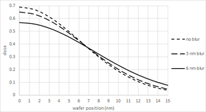
.png)
A study by the College of Nanoscale Science and Engineering (CNSE) presented at the 2013 EUVL Workshop indicated that, as a measure of EUV photoelectron and secondary electron blur, 50–100 eV electrons easily penetrated beyond 15 nm of resist thickness (PMMA or commercial resist), indicating more than 30 nm range of resist affected centered on the EUV point of absorption, for doses exceeding 200–300 uC/cm2.[182] This can be compared with the image contrast degradation reported for sub-40 nm pitches later in 2015.[55]
The process of electron penetration through a resist is essentially a stochastic process; there is a finite probability that resist exposure by released electrons can occur quite far from the point of photon absorption.[183][184] Increasing the dose increases the number of far-reaching electrons, resulting in more extended resist loss. A leading EUV chemically amplified resist exposed to 80 eV electrons at a dose up to 80 uc/cm2 showed up to 7.5 nm resist thickness loss.[185] For an open-source resist exposed near 200 uC/cm2 by 80 eV electrons, the resist thickness lost after post-exposure bake and development was around 13 nm, while doubling the dose resulted in increasing the loss to 15 nm.[52] On the other hand, for doses >500 uC/cm2, the resist begins to thicken due to crosslinking.[185]
The degree of photoelectron emission from the layer underlying the EUV photoresist has been shown to affect the depth of focus.[186] Unfortunately, hardmask layers tend to increase photoelectron emission, degrading the depth of focus.
Secondary electron blur vs. dose
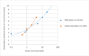

Direct photocurrent measurements have been used to obtain secondary electron yields in response to EUV radiation. Simulations roughly calibrated to this yield show that the secondary electron blur increases with dose.[187] This is associated with fewer trapping sites as dose is increased and the reactions depleting the trapping sites proceed.
Low-energy electron-induced events also increase in number at a given distance from the photon absorption site, as dose is increased. This has been confirmed by resist thickness loss measurements as a function of low-energy electron dose.[188] The dose-dependent spread of secondary electrons was also known before from electron beam lithography.[189]
The increased secondary electron blur with increased dose makes control of stochastic defects more difficult.[190]
Charging and electron trapping
Due to the production of secondary electrons of various energies, the charge of the resist may locally fluctuate.[191] An EUV exposure with less blur leads to more pronounced charge differences at the feature edge,[192] which can lead to larger electric fields.[193] Such large electric fields have been observed to lead to dielectric breakdown.[191] The trapping of secondary electrons leads to a reduction of secondary electrons emitted from the film;[191] however, the trap sites may themselves be depleted, resulting in effectively extended secondary electron blur for larger doses.[187] Electron trapping is predicted to occur as part of polaronic behavior,[194][195] which confines the electron's final energy deposition to trap site locations. The polaron size can be quite large in resists, e.g., 46 nm in PMMA.[195]
DUV sensitivity
EUV resists are also exposable by wavelengths longer than EUV, particular VUV and DUV wavelengths in the 150–250 nm range.[196]
Resist outgassing

Due to the high efficiency of absorption of EUV by photoresists, heating and outgassing become primary concerns. Organic photoresists outgas hydrocarbons[197] while metal oxide photoresists outgas water and oxygen[198] and metal (in a hydrogen ambient); the last is uncleanable.[37] The carbon contamination is known to affect multilayer reflectivity[199] while the oxygen is particularly harmful for the ruthenium capping layers on the EUV multilayer optics.[200]
Contamination effects
One well-known issue is contamination deposition on the resist from ambient or outgassed hydrocarbons, which results from EUV- or electron-driven reactions.[201]
Side effects of hydrogen for contamination removal: tin redeposition, blistering, resist erosion
Atomic hydrogen in the tool chambers is used to clean tin and carbon which deposit on the EUV optical surfaces.[202] The reaction with tin in the light source or resist or on an optical surface to form volatile SnH4 proceeds via the reaction:
Sn(s) + 4H(g) => SnH4(g).[202]
The SnH4 can reach the coatings of other EUV optical surfaces, where it redeposits Sn via the reaction:
SnH4 => Sn(s) + 2H2(g).[202]
Redeposition may also occur by other intermediate reactions.[203]
The redeposited Sn[36][37] might be subsequently removed by atomic hydrogen exposure. However, overall, the tin cleaning efficiency is less than 0.01%, due to both redeposition and hydrogen desorption, leading to formation of hydrogen molecules at the expense of atomic hydrogen.[202]
The removal of carbon proceeds by methane formation at lower temperatures or acetyelene formation at higher temperatures:[202]
H(ads) + C => CH(ads)
Methane formation:
CH(ads) + H(ads) => CH2(ads)
CH2(ads) + H(ads) => CH3(ads)
CH3(ads) + H(ads) => CH4(g)
Acetylene formation:
CH(ads) + CH(ads) => C2H2(g)
Atomic hydrogen is produced by EUV light directly photoionizing H2:
hν + H2 => H+ + H + e−[204]
Electrons generated in the above reaction may also dissociate H2 to form atomic hydrogen:
e− + H2 => H+ + H + 2e−[204]

Hydrogen also reacts with metal-containing compounds to reduce them to metal,[205] and diffuses through the silicon[206] and molybdenum[207] in the multilayer, eventually causing blistering.[208][209] Capping layers that mitigate hydrogen-related damage often reduce reflectivity to well below 70%.[208] Capping layers are known to be permeable to ambient gases including oxygen[210] and hydrogen,[211][212][213][214] as well as susceptible to the hydrogen-induced blistering defects.[215] Hydrogen may also react with the capping layer, resulting in its removal.[216] Hydrogen also reacts with resists to etch[217][218] or decompose[219] them. Besides photoresist, hydrogen plasmas can also etch silicon, albeit very slowly.[220]
Membrane
To help mitigate the above effects, the latest EUV tool introduced in 2017, the NXE:3400B, features a membrane that separates the wafer from the projection optics of the tool, protecting the latter from outgassing from the resist on the wafer.[39] The membrane contains layers which absorb DUV and IR radiation, and transmits 85-90% of the incident EUV radiation. There is of course, accumulated contamination from wafer outgassing as well as particles in general (although the latter are out of focus, they may still obstruct light).
Mask defects
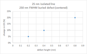
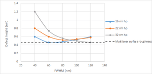
Reducing defects on extreme ultraviolet (EUV) masks is currently one of the most critical issues to be addressed for commercialization of EUV lithography.[221] Defects can be buried underneath or within the multilayer stack[222] or be on top of the multilayer stack. Mesas or protrusions form on the sputtering targets used for multilayer deposition, which may fall off as particles during the multilayer deposition.[223] In fact, defects of atomic scale height (0.3–0.5 nm) with 100 nm FWHM can still be printable by exhibiting 10% CD impact.[224] IBM and Toppan reported at Photomask Japan 2015 that smaller defects, e.g., 50 nm size, can have 10% CD impact even with 0.6 nm height, yet remain undetectable.[225]
Furthermore, the edge of a phase defect will further reduce reflectivity by more than 10% if its deviation from flatness exceeds 3 degrees, due to the deviation from the target angle of incidence of 84 degrees with respect to the surface. Even if the defect height is shallow, the edge still deforms the overlying multilayer, producing an extended region where the multilayer is sloped. The more abrupt the deformation, the narrower the defect edge extension, the greater the loss in reflectivity.
EUV mask defect repair is also more complicated due to the across-slit illumination variation mentioned above. Due to the varying shadowing sensitivity across the slit, the repair deposition height must be controlled very carefully, being different at different positions across the EUV mask illumination slit.[226]
Multilayer damage
Multiple EUV pulses at less than 10 mJ/cm2 could accumulate damage to a Ru-capped Mo/Si multilayer mirror optic element.[227] The angle of incidence was 16° or 0.28 rads, which is within the range of angles for a 0.33 NA optical system.
Pellicles
Production EUV tools need a pellicle to protect the mask from contamination. Currently, the pellicle is not yet guaranteed to withstand 250 W power necessary for high volume manufacturing; the specification is 40 W.[228]
Pellicles are normally expected to protect the mask from particles during transport, entry into or exit from the exposure chamber, as well as the exposure itself. Without pellicles, particle adders would reduce yield, which has not been an issue for conventional optical lithography with 193 nm light and pellicles. However, for EUV, the feasibility of pellicle use is severely challenged, due to the required thinness of the shielding films to prevent excessive EUV absorption. Particle contamination would be prohibitive if pellicles were not stable above 200 W, i.e., the targeted power for manufacturing.[229]
Heating of the EUV mask pellicle (film temperature up to 750 K for 80 W incident power) is a significant concern, due to the resulting deformation and transmission decrease.[230] ASML developed a 70 nm thick polysilicon pellicle membrane, which allows EUV transmission of 82%; however, less than half of the membranes survived expected EUV power levels.[231] SiNx pellicle membranes also failed at 82 W equivalent EUV source power levels.[232] At target 250 W levels, the pellicle is expected to reach 686 degrees Celsius,[233] well over the melting point of aluminum. Alternative materials need to allow sufficient transmission as well as maintain mechanical and thermal stability. However, graphite, graphene or other carbon nanomaterials (nanosheets, nanotubes) are damaged by EUV due to the release of electrons[234] and also too easily etched in the hydrogen cleaning plasma expected to be deployed in EUV scanners.[235] Hydrogen plasmas can also etch silicon as well.[236][237] A coating helps improve hydrogen resistance, but this reduces transmission and/or emissivity, and may also affect mechanical stability (e.g., bulging).[238] The current lack of any suitable pellicle material, aggravated by the use of hydrogen plasma cleaning in the EUV scanner,[239][240] presents an obstacle to volume production.[241]
ASML, the sole EUV tool supplier, reported in June 2019 that pellicles required for critical layers still required improvements.[242]
In the absence of pellicles, EUV mask cleanliness would have to be checked before actual product wafers are exposed, using wafers specially prepared for defect inspection.[243] These wafers are inspected after printing for repeating defects indicating a dirty mask; if any are found, the mask must be cleaned and another set of inspection wafers are exposed, repeating the flow until the mask is clean. Any affected product wafers must be reworked.
Hydrogen bulging defects
As discussed above, with regard to contamination removal, hydrogen used in recent EUV systems can penetrate into the EUV mask layers. Once trapped, bulge defects were produced.[215] These are essentially the blister defects which arise after a sufficient number of EUV mask exposures in the hydrogen environment.
Throughput-scaling limits
The resolution of EUV lithography for the future faces challenges in maintaining throughput, i.e., how many wafers are processed by an EUV tool per day. These challenges arise from smaller fields, additional mirrors, and shot noise. In order to maintain throughput, the power at intermediate focus (IF) must be continually increased.
Reduced fields
Preparation of an anamorphic lens with an NA between 0.5 and 0.6 is underway as of 2016. The demagnification will be 8X in one dimension and 4X in the other, and the angle of reflection will increase.[244]
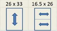
Higher demagnification will increase the mask size or reduce the size of the printed field. Reduced field size would divide full-size chip patterns (normally taking up 26 mm × 33 mm) among two or more conventional 6-inch EUV masks. Large (approaching or exceeding 500 mm2) chips, typically used for GPUs[245] or servers,[246] would have to be stitched together from two or more sub-patterns from different masks.[247] Without field stitching, die size would be limited. With field stitching, features that cross field boundaries would have alignment errors, and the extra time required to change masks would reduce the throughput of the EUV system.[248]
Shot noise: the statistical resolution limit
With the natural Poisson distribution due to the random arrival and absorption times of the photons,[249][250] there is an expected natural dose (photon number) variation of at least several percent 3 sigma, making the exposure process susceptible to stochastic variations. The dose variation leads to a variation of the feature edge position, effectively becoming a blur component. Unlike the hard resolution limit imposed by diffraction, shot noise imposes a softer limit, with the main guideline being the ITRS line width roughness (LWR) spec of 8% (3s) of linewidth.[251] Increasing the dose will reduce the shot noise,[252] but this also requires higher source power.
A 10 nm wide, 10 nm long assist feature region, at a target non-printing dose of 15 mJ/cm2, with 10% absorption, is defined by just over 100 photons, which leads to a 6s noise of 59%, corresponding to a stochastic dose range of 6 to 24 mJ/cm2, which could affect the printability.
A 2017 study by Intel showed that for semi-isolated vias (whose Airy disk can be approximated by a Gaussian), the sensitivity of CD to dose was particularly strong,[253] strong enough that a reduction of dose could nonlinearly lead to failure to print the via.

Minimum dose to restrain shot noise for process variation tolerance areas:
| Tolerance width | Tolerance area | Dose for 3s=7% noise (1800 absorbed EUV photons, 33% absorption) |
|---|---|---|
| 4 nm | 16 nm2 | 496 mJ/cm2 |
| 2 nm | 4 nm2 | 1980 mJ/cm2 |
+ A process variation tolerance area is the largest region over which process variation is allowed.
The two issues of shot noise and EUV-released electrons point out two constraining factors: 1) keeping dose high enough to reduce shot noise to tolerable levels, but also 2) avoiding too high a dose due to the increased contribution of EUV-released photoelectrons and secondary electrons to the resist exposure process, increasing the edge blur and thereby limiting the resolution. Aside from the resolution impact, higher dose also increases outgassing[254] and limits throughput, and crosslinking[255] occurs at very high dose levels. For chemically amplified resists, higher dose exposure also increases line edge roughness due to acid generator decomposition.[256]
As mentioned earlier, a more absorbing resist actually leads to less vertical dose uniformity. This also means shot noise is worse toward the bottom of a highly absorbing EUV resist layer.

Even with higher absorption, EUV has a larger shot noise concern than the ArF (193 nm) wavelength, mainly because it is applied to smaller dimensions and current dose targets are lower due to currently available source power levels.
| Wavelength | Resist type | Absorbance | Thickness | Absorption | Target dose | Absorbed photon dose |
|---|---|---|---|---|---|---|
| ArF (193 nm) | CAR | 1.2/μm[257] | 0.08 μm | 9% | 30 mJ/cm2[258] | 27 photons/nm2 |
| EUV (13.5 nm) | CAR | 5/μm[259] | 0.05 μm | 22% | 30 mJ/cm2[260] | 4.5 photons/nm2 |
| EUV (13.5 nm) | Metal oxide | 20/μm[259] | 0.02 μm | 33% | 30 mJ/cm2[260] | 7 photons/nm2 |
As can be seen above, at the target incident dose levels, significantly fewer EUV photons are absorbed in EUV resists compared to ArF photons in ArF resists. Despite greater transparency of the resist, the incident photon flux is about 14 times larger (193/13.5) for the same energy dose per unit area. The resist thickness is limited by transparency as well as resist collapse[261] and resist strip[262] considerations.
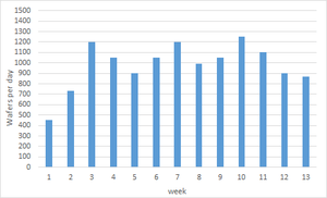
Uptime and productivity
Current throughput at customer site is 1,200 wafers per day with 80% availability,[263] while conventional tools produce 5,000 wafers per day with 95% availability.[264] As of 2017, the cost of a 7 nm process with 3 metal layers patterned by single EUV exposure is still 20% higher than the current 10 nm non-EUV multipatterned process.[265] Hence, multiple patterning with immersion lithography has been deployed for volume manufacturing, while deployment of EUV is expected in 2018–2020.
Deployment history
The deployment of EUVL for volume manufacturing has been delayed for a decade,[266][267] though the forecasts for deployment had timelines of 2–5 years. Deployment was targeted in 2007 (5 years after the forecast was made in 2002),[266] in 2009 (5 years after the forecast), in 2012–2013 (3–4 years), in 2013–2015 (2–4 years),[268][269] in 2016–2017 (2–3 years),[270] and in 2018–2020 (2–4 years after the forecasts).[271][272] However, deployment could be delayed further.[273]
Shipments of the NXE:3350 system began at the end of 2015, with claimed throughput of 1,250 wafers/day or 65 wafers per hour (WPH) assuming 80% uptime.[274][275] By comparison, the 300-unit installed base of NXT 193-nm immersion systems had 96% availability and 275 WPH in 2015.[276][277]
| Year | WPH | Forecast WPH | Availability | Forecast avail. |
|---|---|---|---|---|
| 2014 | 55[278] | 70[279] | 50%[278] | |
| 2015 | 55[280] | 75;[278] 125[279] | 70%[281] | 70%[278] |
| 2016 | 85[281] | 125[279] | 80%[281] | 80%[278] |
| 2017 | 125[281] | 85%[281] | ||
| 2018 | 140[281] | 90%[281] |
Twenty EUV units were shipped in 2010–2016, short of the number that would be required for volume manufacturing. By comparison, ASML shipped over 60 NXT 193-nm immersion systems in 2016, and forecasts that 48 EUV units will be shipped in 2019.[282][283] Six NXE:3100 units were shipped in 2010–2011.[284][285] Eight NXE:3300B units were shipped in 2013Q3–2015Q1,[277] fewer than the forecast 11 units.[286] Two NXE:3350B units were shipped in late 2015,[276] compared to a forecast six units.[277] Four units were shipped in 2016, compared to a forecast six or seven units from the start of the year.[287]
As of 2016, 12 units were forecast to ship in 2017,[287] and 24 units in 2018.[282] However, the shipment forecast for 2017 was halved at the beginning of the year to six or seven units.[288] The NXE:3350B is planned to be discontinued by 2017, to be replaced by the NXE:3400B. At the time of shipping of the first NXE:3400B,[289] eight NXE:3300B and six NXE:3350B systems were up and working in the field.[290]
A total of ten NXE3400B systems were shipped in 2017.[291] In Q1 2018, three EUV systems were shipped.[292] In Q2 2018, 4 more were shipped.[293]
EUV tool sales recognized (ASML quarterly reports)
| Year | Q1 | Q2 | Q3 | Q4 |
|---|---|---|---|---|
| 2017 | 0 | 3 | 4 | 5 |
| 2018 | 1 | 7 | 5 | 5 |
| 2019 | 4 | 7 | 7 (incl. 3 NXE:3400C)[294] | 8 (incl. 6 NXE:3400C)[294][295][296] |
Forty-five (45) NXE:3400B systems in total will be shipped by end of 2019.[1] By comparison, 27 immersion tools were shipped to Samsung in 2010 alone.[297] As of 2011, over 80 immersion tools were being used worldwide for 32-45 nm lithography.[298] As of 2013, over 200 immersion tools were being used, in anticipation of 14-20nm nodes.[2] Intel had around 200 SVG Micrascan DUV tools to support 200mm manufacturing.[299] Thus, EUV volume is negligible compared to DUV use at mature nodes.
ASML expects to ship about 35 EUV systems in 2020 and between 45 and 50 EUV systems in 2021.[295]
Ongoing issues for improvement
The NXE:3400C was announced to be introduced in 2019, including features that focused on improving uptime significantly, such as a modular design for faster changing, continuous tin supply, and better collector degradation control.[300] However, aberration improvements have yet to be implemented, as aberrations have to be measured directly in-situ first.[301]
ASML plans to introduce an improved EUV system late 2021.[302] It will be called NXE:3600[303] and based on previous roadmaps it should improve throughput to over 185 wafers per hour and have an overlay of 1.1 nm.
Use with multiple patterning
EUV is anticipated to use double patterning at around 34 nm pitch with 0.33 NA.[304][305] This resolution is equivalent to '1Y' for DRAM.[306][307] In H2 2018, TSMC confirmed that its 5 nm EUV scheme still used multi-patterning,[308] also indicating that mask count did not decrease from its 7 nm node, which used extensive DUV multi-patterning, to its 5 nm node, which used extensive EUV.[309] EDA vendors also indicated the continued use of multi-patterning flows.[310][311] While Samsung introduced its own 7 nm process with EUV single patterning,[312] it encountered severe photon shot noise causing excessive line roughness, which required higher dose, resulting in lower throughput.[249] TSMC's 5 nm node uses even tighter design rules.[313] Samsung indicated smaller dimensions would have more severe shot noise.[249]
In Intel's complementary lithography scheme at 20 nm half-pitch, EUV would be used only in a second line-cutting exposure after a first 193 nm line-printing exposure.[314]
Multiple exposures would also be expected where two or more patterns in the same layer, e.g., different pitches or widths, must use different optimized source pupil shapes.[315][316][317][318] For example, when considering a staggered bar array of 64 nm vertical pitch, changing the horizontal pitch from 64 nm to 90 nm changes the optimized illumination significantly.[40] Source-mask optimization that is based on line-space gratings and tip-to-tip gratings only does not entail improvements for all parts of a logic pattern, e.g., a dense trench with a gap on one side.[319][320]
For the 24-36 nm metal pitch, it was found that using EUV as a (second) cutting exposure had a significantly wider process window than as a complete single exposure for the metal layer.[321][319]
Multiple exposures of the same mask are also expected for defect management without pellicles, limiting productivity similarly to multiple patterning.[243]
Single patterning extension: anamorphic high-NA
A return to extended generations of single exposure patterning would be possible with higher numerical aperture (NA) tools. An NA of 0.45 could require retuning of a few percent.[322] Increasing demagnification could avoid this retuning, but the reduced field size severely affects large patterns (one die per 26 mm × 33 mm field) such as the many-core multi-billion transistor 14 nm Xeon chips.[323] by requiring field stitching.
In 2015, ASML disclosed details of its anamorphic next-generation EUV scanner, with an NA of 0.55. The demagnification is increased from 4x to 8x only in one direction (in the plane of incidence).[324] However, the 0.55 NA has a much smaller depth of focus than immersion lithography.[325] Also, an anamorphic 0.52 NA tool has been found to exhibit too much CD and placement variability for 5 nm node single exposure and multi-patterning cutting.[326]
Depth of focus[327] being reduced by increasing NA is also a concern,[328] especially in comparison with multipatterning exposures using 193 nm immersion lithography:
| Wavelength | Refractive index | NA | DOF (normalized)[327] |
|---|---|---|---|
| 193 nm | 1.44 | 1.35 | 1 |
| 13.3-13.7 nm | 1 | 0.33 | 1.17 |
| 13.3-13.7 nm | 1 | 0.55 | 0.4 |
The first high-NA tools are expected by 2020 at earliest.[329]
Beyond EUV wavelength
A much shorter wavelength (~6.7 nm) would be beyond EUV, and is often referred to as BEUV (beyond extreme ultraviolet).[330] A shorter wavelength would have worse shot noise effects without ensuring sufficient dose.[331]
References
- "ASML Starts NXE:3400C Shipment, But Supply Constraints Loom". October 17, 2019.
- ASML Q2 2013 report.
- ISS 2020 outlook for EUV
- "EUV tool costs hit $120 million". EETimes. November 19, 2010.
- "Leading Chipmakers Eye EUV Lithography to Save Moore's Law". IEEE Spectrum. October 31, 2016. "The list price of ASML’s newest EUV machine exceeds €100 million"
- "Why EUV Is So Difficult". November 17, 2016.
- https://www.nist.gov/sites/default/files/documents/pml/div683/conference/Rice_2011.pdf
- Montcalm, C. (March 10, 1998). "Multilayer reflective coatings for extreme-ultraviolet lithography". OSTI 310916. Cite journal requires
|journal=(help) - "Next EUV Issue: Mask 3D Effects". April 25, 2018.
- "AGC to Further Expand its Supply System for EUVL Mask Blanks | News | AGC". AGC.
- "Semiconductor Engineering - EUV Mask Blank Battle Brewing". November 15, 2018.
- "ULTRA Semiconductor Laser Mask Writer | Heidelberg Instruments". www.himt.de.
- "MeRiT® neXT". www.zeiss.com.
- "Centura® Tetra™ EUV Advanced Reticle Etch | Applied Materials". www.appliedmaterials.com.
- "EUV collector cleaning" (PDF).
- H. Komori et al., Proc. SPIE 5374, pp. 839–846 (2004).
- B. A. M. Hansson et al., Proc. SPIE 4688, pp. 102–109 (2002).
- S. N. Srivastava et al., J. Appl. Phys.' 102, 023301 (2007).
- "H. S. Kim, Future of Memory Devices and EUV Lithography, 2009 EUV Symposium" (PDF). Archived from the original (PDF) on 2015-07-10. Retrieved 2012-10-25.
- H. Mizoguchi, "Laser Produced Plasma EUV Light Source Gigaphoton Update," EUVL Source Workshop, May 12, 2008.
- "Cookies op ed.nl | ed.nl".
- "Gigaphoton" (PDF).
- "Cymer SPIE 2018" (PDF).
- "Zeiss 2018 EUVL Workshop update" (PDF).
- "SPIE 2007 paper" (PDF).
- "ASML, 2016 EUVL Workshop, p.14" (PDF).
- Y. Wang and Y. Liu, Proc. SPIE 9283, 928314 (2014).
- "R. Capelli et al., Proc. SPIE 9231, 923109 (2014)" (PDF).
- "M. van den Brink et al., Proc. SPIE 2726 (1996)" (PDF).
- Schmoeller, Thomas; Klimpel, T; Kim, I; F. Lorusso, G; Myers, A; Jonckheere, Rik; Goethals, Anne-Marie; Ronse, K (14 March 2008). "EUV pattern shift compensation strategies - art. no. 69211B". Proceedings of SPIE. 6921. doi:10.1117/12.772640 – via ResearchGate.
- A. N. Broers, IEEE Trans. Elec. Dev. 28, 1268 (1981).
- Tao, Y.; et al. (2005). "Characterization of density profile of laser-produced Sn plasma for 13.5 nm extreme ultraviolet source". Appl. Phys. Lett. 86 (20): 201501. Bibcode:2005ApPhL..86t1501T. doi:10.1063/1.1931825.
- "Abstract 107 Last Page". www.nifs.ac.jp.
- I. Fomenkov et al., Adv. Opt. Tech. 6, 173 (2017).
- I. V. Fomenkov, Proc. SPIE 10957, 1095719 (2019).
- "Rutgers University Department of Physics and Astronomy" (PDF). www.physics.rutgers.edu. Archived from the original (PDF) on 2016-12-20. Retrieved 2016-12-14.
- "Metal outgassing study at EIDEC" (PDF).
- R. Rokitski et al., Proc. SPIE 7640, 76401Q (2010).
- M. van de Kerkhof et al., Proc. SPIE 10143, 101430D (2017).
- Y. Chen et al., J.Vac. Sci. Tech. B35, 06G601 (2017).
- "H. Mizoguchi et al., 2017 EUV-FEL Workshop, p. 4" (PDF).
- "M. A. van den Brink et al., Proc. SPIE 2726, 734 (1996)" (PDF).
- Paetzel, R.; et al. (2003). Yen, Anthony (ed.). "Excimer lasers for superhigh NA 193-nm lithography". Proc. SPIE. Optical Microlithography XVI. 5040: 1665. Bibcode:2003SPIE.5040.1665P. doi:10.1117/12.485344.
- Harilal, S. S.; et al. (2006). "Spectral control of emissions from tin doped targets for extreme ultraviolet lithography". J. Phys. D. 39 (3): 484–487. Bibcode:2006JPhD...39..484H. doi:10.1088/0022-3727/39/3/010. S2CID 34621555.
- T. Asayama et al., Proc. SPIE vol. 8683, 86831G (2013).
- "ASML update Nov. 2013, Dublin" (PDF).
- P. De Bisschop, “Stochastic effects in EUV lithography: random, local CD variability, and printing failures”, J. Micro/Nanolith. MEMS MOEMS 16(4), 041013 (2017).
- P. De Bisschop and E. Hendrickx, Proc. SPIE 10583, 105831K (2018).
- The Stochastic Variation of EUV Source Illumination
- The Stochastic Impact of Defocus in EUV Lithography
- The Stochastic Impact of Defocus in EUV Lithography
- A. Narasimhan et al., Proc. SPIE 9422, 942208 (2015).
- Fukuda, Hiroshi (February 23, 2019). "Localized and cascading secondary electron generation as causes of stochastic defects in extreme ultraviolet projection lithography". Journal of Micro/Nanolithography, MEMS, and MOEMS. 18 (1): 013503. Bibcode:2019JMM&M..18a3503F. doi:10.1117/1.JMM.18.1.013503.
- L. Meli et al., J. Micro/Nanolith. MEMS MOEMS 18, 011006 (2019).
- N. Felix et al., Proc. SPIE 9776, 97761O (2015).
- "S. Bhattarai, PhD Thesis,"Study of Line Edge Roughness and Interactions of Secondary Electrons in Photoresists for EUV Lithography," U. Calif. Berkeley, 2017" (PDF).
- S. Larivière et al., Proc. SPIE 10583, 105830U (2018).
- "From Shot Noise to Stochastic Defects: Dose-Dependent Gaussian Blur in Lithography". www.linkedin.com.
- Y. Chen et al., Proc. SPIE 10143, 101431S (2017).
- J. Ruoff, Proc. SPIE 7823, 78231N (2010).
- George, Simi A.; Nauleau, Patrick; Rekawa, Senajith; Gullikson, Eric; Kemp, Charles D. (February 23, 2009). Schellenberg, Frank M; La Fontaine, Bruno M (eds.). "Out-of-band exposure characterization with the SEMATECH Berkeley 0.3-NA microfield exposure tool". Journal of Micronano Lithography, MEMS and MOEMS. Alternative Lithographic Technologies. 7271: 72710X. Bibcode:2009SPIE.7271E..0XG. doi:10.1117/12.814429. OSTI 960237.
- "Measurement and characterization of EUV mask performance at high-NA | EECS at UC Berkeley". www2.eecs.berkeley.edu.
- "Carl Zeiss SMT GMbH, Semicon Europa, Nov. 16 2018" (PDF).
- "Multilayer Reflectivity". henke.lbl.gov.
- Y. Nakajima et al., Proc. SPIE 7379, 73790P (2009).
- N. Davydova et al., Proc. SPIE 8166, 816624 (2011).
- G. J. Stagaman et al., Proc. SPIE 2726, 146 (1996).
- M.F. Ravet et al., Proc. SPIE 5250, 99 (2004).
- F. Scholze et al., Proc. SPIE 6151, 615137 (2006).
- "[PDF] Properties of broadband depth-graded multilayer mirrors for EUV optical systems. | Semantic Scholar". doi:10.1364/OE.18.006957. PMID 20389715. S2CID 16163302. Cite journal requires
|journal=(help) - Chromatic Blur in EUV Lithography
- "The Very Different Wavelengths of EUV Lithography". www.linkedin.com.
- M. Sugawara et al., J. Micro/Nanolith. MEMS MOEMS 2, 27-33 (2003).
- https://www.linkedin.com/pulse/uncertain-phase-shifts-euv-masks-frederick-chen
- M. Burkhardt et al., Proc. SPIE 10957, 1095710 (2019).
- A. Erdmann, P. Evanschitzky, T. Fuhrer, Proc. SPIE 7271, 72711E (2009).
- L. Peters, "Double Patterning Leads Race for 32 nm", Semiconductor International, October 18, 2007.
- M. Sugawara et al., J. Vac. Sci. Tech. B 21, 2701 (2003).
- "Proceedings" (PDF). doi:10.1117/12.484986. Cite journal requires
|journal=(help) - G. McIntyre et al., Proc. SPIE vol. 7271, 72711C (2009).
- T. Last et al., Proc. SPIE 9985, 99850W (2016).
- T. Last et al., Proc. SPIE vol. 10143, 1014311 (2017).
- W. Gao et al., Proc. SPIE vol. 10143, 101430I (2017).
- "EUV Mask Flatness Requirements" (PDF). Archived from the original (PDF) on 2015-06-26. Retrieved 2015-06-26.
- T. Schmoeller et al., Proc. SPIE vol. 6921, 69211B (2008).
- P. Liu et al., Proc. SPIE vol. 8679, 86790W (2013).
- M. Sugawara et al., Proc. SPIE 9048, 90480V (2014).
- X. Chen et al., Proc. SPIE 10143, 101431F (2017).
- "ASML: Products - TWINSCAN NXE:3400B". asml.com.
- X. Liu et al., Proc. SPIE vol. 9048, 90480Q (2014).
- O. Wood et al., Proc. SPIE 10450, 1045008 (2017).
- S. Yoshitake et al., EUV Mask Flatness Requirements: E-beam Mask Writer Supplier Perspective.
- H. N. Chapman and K. A. Nugent, Proc. SPIE 3767, 225 (1999).
- H. Komatsuda, Proc. SPIE 3997, 765 (2000).
- Q. Mei et al., Proc. SPIE 8679, 867923 (2013).
- D. Hellweg et al., Proc. SPIE 7969, 79690H (2011).
- K. Hooker et al., Proc. SPIE 10446, 1044604 (2017).
- A. Garetto et al., J. Micro/Nanolith. MEMS MOEMS 13, 043006 (2014).
- T-S. Eom et al., Proc. SPIE 8679, 86791J (2013).
- R. Capelli et al., Proc. SPIE 10957, 109570X (2019).
- S. Koo et al., Proc. SPIE 7969, 79691N (2011).
- US Patent Application 20070030948.
- D. M. Williamson, Proc. SPIE 3482, 369 (1998).
- "Carl Zeiss 2018" (PDF).
- S. D. Hsu et al. (ASML), Semicon Taiwan 2015.
- L. van Look et al., Proc. SPIE 10809, 108090M (2018)
- R-H. Kim et al., Proc. SPIE 9776, 97761R (2016).
- E. van Setten et al., Proc. SPIE 9661, 96610G (2015).
- T. E. Brist and G. E. Bailey, Proc. SPIE 5042, 153 (2003).
- G. Zhang et al., Proc. SPIE 5040, 45 (2003).
- K. A. Goldberg et al., Proc. SPIE 5900, 59000G (2005).
- Y. Liu and Y. Li, Opt. Eng. 55, 095108 (2016).
- R., Saathof (1 December 2018). "Adaptive Optics to Counteract Thermal Aberrations: System Design for EUV-Lithography with Sub-nm Precision". Cite journal requires
|journal=(help) - T. S. Jota and R. A. Chipman, Proc. SPIE 9776, 977617 (2016).
- "Mentor Graphics Director Details Challenges for Edge Placement Control in 2020". nikonereview.com.
- M. Habets et al., Proc. SPIE 9776, 97762D (2016).
- M. Bayraktar et al., Opt. Exp. 22, 30623 (2014).
- J. Heo et al., Opt. Exp. 25, 4621 (2017).
- C. S. Choi et al., Proc. SPIE 9235, 92351R (2014).
- Fundamental Principles of Optical Lithography Chris A. Mack, p. 37.
- C. A. Mack, Microlith. World, 9-4, 25 (2000)
- J. S. Petersen et al., Proc. SPIE 3546, 288 (1998).
- "Archived copy" (PDF). Archived from the original (PDF) on 2017-02-05. Retrieved 2017-02-05.CS1 maint: archived copy as title (link)
- Thin Half-tone Phase Shift Mask Stack for Extreme Ultraviolet Lithography Inhwan Lee, Sangsul Lee, Jae Uk Lee, Chang Young Jeong2, Sunyoung Koo, Changmoon Lim, and Jinho Ahn
- L. Yuan et al., Proc. SPIE 8322, 832229 (2012).
- "Study of Line Edge Roughness and Interactions of Secondary Electrons in Photoresists for EUV Lithography | EECS at UC Berkeley".
- Anderson, Christopher; Daggett, Joe; Naulleau, Patrick (31 December 2009). "Corner rounding in EUV photoresist: tuning through molecular weight, PAG size, and development time". OSTI 982925. Cite journal requires
|journal=(help) - E. van Setten et al., Intl. Symp. on EUV Lithography, 2014.
- V. M. Blanco Carballo et al., Proc. SPIE 10143, 1014318 (2017).
- E. van Setten et al., Proc. SPIE 9231, 923108 (2014).
- K. van Ingen Schenau, 2013 EUVL Symposium.
- "SemiWiki.com - SEMICON West - Advanced Interconnect Challenges". www.semiwiki.com.
- "SemiWiki.com - Exclusive - GLOBALFOUNDRIES discloses 7nm process detail". www.semiwiki.com.
- L. T. Clark et al., Microelec. Journ. 53, 105 (2016).
- "ASML 2014 Investor Day slide 46" (PDF).
- F. Jiang et al., Proc. SPIE vol. 9422, 94220U (2015).
- I. Mochi et al., Proc. SPIE 9776, 97761S (2015).
- J. G. Garofalo et al., Proc. SPIE 2440, 302 (1995).
- "Understanding EUV Shot Noise".
- D. Civay et al., Proc. SPIE 9048, 90483D (2014).
- T. Last et al., J. Micro/Nanolith. MEMS MOEMS 15, 043508 (2016).
- "Stochastic Printing of Sub-Resolution Assist Features". www.linkedin.com.
- A-Y. Je et al., Proc. SPIE 7823, 78230Z (2010).
- T. Huynh-Bao et al., Proc. SPIE 9781, 978102 (2016).
- V. Philipsen et al., Proc. SPIE 9235, 92350J (2014).
- W. Gillijns et al., Proc. SPIE 10143, 1014314 (2017).
- Y-G Wang et al., Proc. SPIE 10143, 1014320 (2017).
- US Patent 9715170.
- S. Nagahara et al., Proc. SPIE 7640, 76401H (2010).
- L. Pang et al., Proc. SPIE 7520, 75200X (2009).
- Hsu, Stephen D.; Liu, Jingjing (1 January 2017). "Challenges of anamorphic high-NA lithography and mask making". Advanced Optical Technologies. 6 (3–4): 293. Bibcode:2017AdOT....6..293H. doi:10.1515/aot-2017-0024.
- "Semicon/Japan 99" (PDF).
- Image formation. Number of diffracted orders. (Spatial Fourier components) 2002 November 20
- "IMEC EUVL 2018 Workshop" (PDF).
- C. Krautschik et al., Proc. SPIE 4343, 392 (2001).
- A. Erdmann, P. Evanschitzky, and T. Fuhner, Proc. SPIE 7271, 72711E (2009).
- A. Erdmann et al., J. Micro/Nanolith. MEMS MOEMS 15, 021205 (2016).
- M. Burkhardt and A. Raghunathan, Proc. SPIE 9422, 94220X (2015).
- Z. Zhu et al., Proc. SPIE 5037, 494 (2003)
- V. Philipsen et al., Proc. SPIE 10143, 1014310 (2017).
- "Download Limit Exceeded". CiteSeerX 10.1.1.215.7131. Cite journal requires
|journal=(help) - A. Erdmann et al., J. Micro/Nanolith. MEMS MOEMS 15(2), 021205 (2016).
- L. Liebmann et al. Proc. SPIE 10148, 101480F (2017).
- V. Phiipsen et al., Proc. SPIE 10143, 104310(2017).
- C-H. Chang et al., Proc. SPIE 5377, 902 (2004).
- T. Devoivre et al., MTDT 2002.
- L. C. Choo et al., Proc. SPIE vol. 4000, 1193 (2000).
- J. Word and K. Sakajiri, Proc. SPIE 6156, 61561I (2006).
- T. Winkler et al., Prod. SPIE 5754, 1169 (2004).
- Y. Borodovsky et al., Proc. SPIE 4754, 1 (2002).
- S-S. Yu et al., Proc. SPIE 8679, 86791L (2013).
- A. Erdmann et al., Proc. SPIE 10583, 1058312 (2018).
- "Eigenmode analysis of EM fields in EUV masks" (PDF).
- "Ultra-high efficiency EUV etched phase-shift mask" (PDF).
- ". Torok et al., "Secondary Electrons in EUV Lithography", J. Photopol. Sci. and Tech., 26, 625 (2013)".
- K. Ishii and T. Matsuda, Jpn. J. Appl. Phys. 29, 2212 (1990).
- A. Thete et al., Proc. SPIE 9422, 94220A (2015).
- "B. Sun thesis, p. 34" (PDF).
- "S. Bhattarai, Study of Line Edge Roughness and Interactions of Secondary Electrons in Photoresists for EUV Lithography, 2017, p. 100" (PDF). Archived from the original (PDF) on 2017-10-21. Retrieved 2018-09-16.
- "O. Kostko, J. Ma and P. Naulleau (LBNL), "Measurement of electron blur," 2019 EUVL Workshop" (PDF).
- B. L. Henke et al., J. Appl. Phys. 48, pp. 1852–1866 (1977).
- "CNSE 2013 International Workshop on EUV Lithography" (PDF).
- J. Torok et al., J. Photopolymer Sci. & Tech., 27, 611 (2014).
- Low Energy Electron Set the Limits for EUV Lithography
- Y. Kandel et al., Proc. SPIE 10143, 101430B (2017).
- D. D. Simone et al., Proc. SPIE 10143, 101430R (2017).
- P. De Schepper et al., Proc. SPIE 9425, 942507 (2015).
- A. Narasimhan et al., "Mechanisms of EUV Exposure: Internal Excitation and Electron Blur", EUV Symposium 6/16/2016, p.11.
- A. Raghunathan and J. G. Hartley, JVST B 31, 011605 (2013).
- "EUV's Stochastic Valley of Death". www.linkedin.com.
- A. Thete et al., Phys. Rev. Lett. 266803 (2017).
- L. Wisehart et al., Proc. SPIE 9776, 97762O (2016).
- "Electric Field, Flat Sheets of Charge". hyperphysics.phy-astr.gsu.edu.
- M. Dapor, M. Ciappa, and W. Fichtner, J. Micro/Nanolith. MEMS MOEMS 9, 023001 (2010).
- Z. G. Song et al., J. Phys. D: Appl. Phys. 30, 1561 (1997).
- J. M. Roberts et al., Proc. SPIE 7273, 72731W (2009).
- G. Denbeaux et al., 2007 European Mask and Lithography Conference.
- I. Pollentier et al., Proc. SPIE vol. 7972, 797208 (2011).
- G. Denbeaux, 2009 Intl. Workshop on EUV Lithography.
- J. Y. Park et al., J. Vac. Sci. Tech. B29, 041602 (2011).
- J. Hollenshead and L. Klebanoff, J. Vac. Sci. & Tech. B 24, pp. 118–130 (2006).
- "H atom based tin cleaning" (PDF).
- Computer modeling of contamination and cleaning of EUV source optics RnD-ISAN/EUV Labs & ISTEQ BV
- T. Van de Ven et al., J. Appl. Phys. 123, 063301 (2018).
- e.g., The Denitridation of Nitrides Under Hydrogen
- "C. G. van de Walle and B. Tuttle, THEORY OF HYDROGEN INTERACTIONS WITH AMORPHOUS SILICON in Amorphous and Heterogeneous Silicon Thin Films — Fundamentals to Devices, edited by H. M. Branz, R. W. Collins, H. Okamoto, S. Guha, and B. Schropp, MRS Symposia Proceedings, Vol. 557 (MRS, Pittsburgh, Pennsylvania, 1999), p. 255" (PDF).
- T. Tanabe, Y. Yamanishi, and S. Imoto, J. Nucl. Mat. 191-194, 439 (1992).
- "D. T. Elg et al., J. Vac. Sci. Tech. A 34, 021305 (2016)" (PDF).
- "Hydrogen-induced blistering in thin film multilayers" (PDF).
- I-Y. Jang et al., Proc. SPIE 9256, 92560I (2014)
- "Hydrogen penetration of Ru and Pd/Ru" (PDF).
- Pantisano, L; Schram, Tom; Li, Z; Lisoni, Judit; Pourtois, Geoffrey; De Gendt, Stefan; P. Brunco, D; Akheyar, A; Afanas'ev, V.V.; Shamuilia, Sheron; Stesmans, A (12 June 2006). "Ruthenium gate electrodes on SiO2 and HfO2: Sensitivity to hydrogen and oxygen ambients". Applied Physics Letters. 88 (24): 243514. Bibcode:2006ApPhL..88x3514P. doi:10.1063/1.2212288 – via ResearchGate.
- "Hydrogen penetration of boron carbide".
- M. Mayer, M. Balden, and R. Behrisch, J. Nucl. Mat. 252, 55 (1998).
- S-S. Kim et al., Proc. SPIE 10143, 1014306 (2017).
- "Screening of oxidation-resistance capping layers" (PDF).
- B. Thedjoisworo et al., J. Vac. Sci. Tech. A 30, 031303 (2012).
- "Hydrogen plasma for photoresist stripping" (PDF).
- "Metal Oxide Resist Outgassing" (PDF).
- Thedjoisworo, Bayu; Cheung, David; Crist, Vince (2013). "Comparison of the effects of downstream H2- and O2-based plasmas on the removal of photoresist, silicon, and silicon nitride". Journal of Vacuum Science & Technology B, Nanotechnology and Microelectronics: Materials, Processing, Measurement, and Phenomena. 31 (2): 021206. Bibcode:2013JVSTB..31b1206T. doi:10.1116/1.4792254. ISSN 2166-2746.
- "Getting up to speed with roadmap requirements for extreme-UV lithography". spie.org.
- "Fast Simulation Methods for Non-Planar Phase and Multilayer Defects in DUV and EUV Photomasks for Lithography". berkeley.edu.
- H. Yu et al., J. Vac. Sci. Tech. A31, 021403 (2013).
- S. Huh et al., Proc. SPIE 7271 (2009).
- K. Seki et al., Proc. SPIE 9658, 96580G (2015).
- A. Garetto et al., J. Micro/Nanolith. MEMS MOEMS 13, 043006 (2014).
- M. Muller et al., Appl. Phys. A vol. 108, 263 (2012).
- "2016 EUV Mask Pellicle TWG update" (PDF).
- "EUVL activities in South Korea (including Samsung and SKHynix)" (PDF).
- I-S. Kim et al., Proc. SPIE vol. 8322, 83222X (2012).
- C. Zoldeski et al., Proc. SPIE vol. 9048, 90481N (2014).
- D. L. Goldfarb, Dec. 2015 BACUS Newsletter.
- "EUV Pellicle, Uptime And Resist Issues Continue".
- A. Gao et al., J. Appl. Phys. 114, 044313 (2013).
- E. Gallagher et al., Proc. SPIE vol. 9635, 96350X (2015).
- C. Ghica et al., Rom. Rep. in Phys., vol. 62, 329-340 (2010).
- L. Juan et al., Chin. Phys. B, vol., 22, 105101 (2013).
- I. Pollentier et al., Proc. SPIE vol. 10143, 101430L (2017).
- H. Oizumi et al., Proc. SPIE vol. 5751, 1147 (2005).
- K. Motai et al., Proc. SPIE vol. 6517, 65170F (2007).
- Y. Nagaoka and J. Miyazaki, Proc. SPIE vol. 9635, 963510 (2015).
- "UBS Korea Conference, June 24 2019" (PDF).
- H. J. Levinson and T. A. Brunner, Proc. SPIE 10809, 1080903 (2018).
- "5nm Fab Challenges". 2016-01-20.
ASML is developing an anamorphic lens for EUV. The two-axis EUV lens would support 8x magnification in the scan mode and 4x in the other direction. It would support 0.5 to 0.6 NAs. … The EUV scanner could take a throughput hit. It would expose the wafer at only half the field size, as opposed to full field sizes with today’s EUV scanners.
- Hilbert Hagedoorn. "GeForce GTX 780 review". Guru3D.com.
- Intel Xeon E5-2600 v3
- J. T. Neumann et al., Proc. SPIE vol. 8522, 852211 (2012).
- K. Takehisa, Proc. SPIE vol. 8701, 87010T (2013).
- H-W Kim et al., Proc. SPIE 7636, 76360Q (2010).
- S-M. Kim et al., Proc. SPIE 9422, 94220M (2015).
- B. Baylav, "Reduction of Line Edge Roughness (LER) in Interference-Like Large Field Lithography", PhD dissertation, p. 37, 2014.
- Z-Y. Pan et al., Proc. SPIE 6924, 69241K (2008).
- R. L. Bristol and M. E. Krysak, Proc. SPIE 10143, 101430Z (2017).
- "2013 Nissan Chemical Industries, 2013 International Workshop on EUV Lithography" (PDF).
- T. G. Oyama et al., Appl. Phys. Exp. 7, 036501 (2014).
- T. Kozawa, Jpn. J. Appl. Phys. 51, 06FC01 (2012).
- "Photoresist ABCs" (PDF).
- "ASML: Products - TWINSCAN NXT:1980Di". www.asml.com.
- "EUV Photoresists" (PDF).
- "ASML 2016 EUVL Workshop" (PDF).
- "New solutions for resist" (PDF). Archived from the original (PDF) on 2017-08-27. Retrieved 2017-07-14.
- "Metal oxide resist strip" (PDF).
- 2016 EUV source workshop, ASML update.
- Tartwijk, Stu Woo and Maarten van. "Can This Little-Known Chip Company Preserve Moore's Law?".
- V. M. Blanco Carballo et al., Proc. SPIE 10143, 1014318 (2017).
- http://www.lithoguru.com/scientist/essays/100WbytheEndoftheYear.ppsx
- "Archived copy". Archived from the original on 2016-07-24. Retrieved 2016-08-01.CS1 maint: archived copy as title (link)
- tweet_btn(), Rik Myslewski 25 Feb 2014 at 22:16. "First 'production-ready' EUV scanner laser-fries its guts at TSMC. Intel seeks alternative tech". www.theregister.co.uk.
- "Archived copy". Archived from the original on 2016-08-18. Retrieved 2016-08-01.CS1 maint: archived copy as title (link)
- "TSMC orders production EUV systems". optics.org.
- "ASML boosted by extreme UV orders". optics.org.
- "EUV | Semiconductor Manufacturing & Design Community". semimd.com.
- "ASML Has Record Revenue for 2015; Will Raise Dividend, Buy Back More Stock | Semiconductor Manufacturing & Design Community".
- Tiernan Ray. "ASML Gets a Lift From TSM, Though Questions on EUV Remain". Barrons.
- "asml20160120presentation". www.sec.gov.
- "asml20150715presentation". www.sec.gov.
- Frits van Hout (November 24, 2014). "EUV". ASML. Retrieved December 14, 2016.
- ASML. "ASML reports 2013 results". US Securities and Exchange Commission. Retrieved 2014-07-16.
We remain on target to deliver EUV systems with a throughput of 70 wafers per hour in 2014, upgradeable to 125 wafers per hour in 2015.
- "asml20151014presentation". www.sec.gov.
- Hans Meiling (October 31, 2016). "Role of EUV and its Business Opportunity" (PDF). ASML. Retrieved December 15, 2016.
- "ASML firms up EUV lithography expectations". October 19, 2016.
- "Asml20170118presentation".
- R. Peeters et al., Proc. SPIE 8679, 86791F (2013).
- "Holistic lithography for EUV: NXE:3100 characterization of first printed wafers using an advanced scanner model and scatterometry" (PDF). Archived from the original (PDF) on 2015-07-16. Retrieved 2015-07-16.
- "ASML delays EUV tool revenue recognition". 2012-04-18.
- "ASML confident of 2016 EUV goals; Dutch lithography giant expects to ship at least six systems as customers target 2018 production ramp". 2016-01-20.
- "ASML Holding's (ASML) CEO Peter Wennink on Q4 2016 Results - Earnings Call Transcript". 2017-01-18.
- Merritt, Rick. "ASML Revs EUV Engines". EETimes.
- Merritt, Rick. "EUV Progress, Hurdles Cited". EETimes.
- "2018 SPIE Advanced Lithography – EUVL Conference Update - EUVL Focus". electroiq.com. Archived from the original on 2019-01-26. Retrieved 2018-04-16.
- "ASML: Press - Press ReleasesStrong DUV Demand Drives Solid Q1 Results and Confirms Positive Outlook for 2018 - Multiple EUV Orders, Including High-NA, Demonstrate Further Adoption of EUV Technology - Press ReleasesStrong DUV Demand Drives Solid Q1 Results and Confirms Positive Outlook for 2018 - Multiple EUV Orders, Including High-NA, Demonstrate Further Adoption of EUV Technology". www.asml.com.
- "ASML: Press - Press ReleasesEarnings Growth Continues, Driven by Strong Sales Across Full Product Portfolio - Continued EUV Progress Enables ASML Roadmap Acceleration - Press ReleasesEarnings Growth Continues, Driven by Strong Sales Across Full Product Portfolio - Continued EUV Progress Enables ASML Roadmap Acceleration". www.asml.com.
- ASML Q3 2019 Earnings Call
- "Q4 2019 and full year financial results". www.asml.com. Retrieved 2020-01-22.
- ASML Q4 2019 Earnings Call Transcript
- "ASML, Nikon battle over Intel litho biz" Check
|url=value (help). .. - "ASML enhances NXT:1950i immersion lithography platform". www.fabtech.org.
- Images, Intel Special Edition, ASML, 2006.
- "De 3400C is de euv-machine die ASML altijd heeft willen bouwen – Bits&Chips". bits-chips.nl.
- M. van de Kerkhof et al., Proc. SPIE 10583, 105830S (2018).
- De Young, Craig (March 20, 2019). "BAML 2019 APAC TMT Conference" (PDF). ASML.
- "ASML hiring Architect Extreme Ultraviolet Projection in Veldhoven, NL | LinkedIn". nl.linkedin.com. Retrieved 2019-12-24.
- W. Gap et al., Proc. SPIE 10583, 105830O (2018).
- D. De Simone et al., Advanced Lithography 2019, 10957-21.
- "Samsung 18 nm DRAM cell integration: QPT and higher uniformed capacitor high-k dielectrics". techinsights.com.
- Roos, Gina (May 24, 2018). "Prices for DRAMs Continue to Climb while NAND Flash ASPs Drop".
- "SemiWiki.com - Top 10 Highlights from the TSMC Open Innovation Platform Ecosystem Forum". www.semiwiki.com.
- "DAC 2018 TSMC/Arm/Synopsys Breakfast". www.synopsys.com.
- "Cadence Achieves EDA Certification for TSMC 5nm and 7nm+ FinFET Process Technologies to Facilitate Mobile and HPC Design Creation". October 2018.
- "Synopsys Digital and Custom Design Platforms Certified on TSMC 5-nm EUV-based Process Technology". Design And Reuse.
- "DAC 2018 Samsung/Synopsys Breakfast". www.synopsys.com.
- Merritt, Rick. "TSMC Goes Photon to Cloud". EETimes.
- "Intel presentation on Complementary Lithography at 2012 International Workshop on EUV Lithography" (PDF).
- "EUV was never going to be single patterning".
- S. Hsu et al., Proc. SPIE 4691, 476 (2002).
- X. Liu et al., Proc. SPIE 9048, 90480Q (2014).
- S-Y. Oh et al., Proc. SPIE 4691, 1537 (2002).
- "EUV was never going to be single patterning". www.semiwiki.com.
- D. Rio et al., Proc. SPIE 10809, 108090N (2018).
- R. K. Ali et al., Proc. SPIE 10583, 1058321 (2018).
- J. T. Neumann et al., Proc. SPIE 8522, 852211 (2012).
- Intel’s Xeon E5-2600 V4 Chips Feature An Insane 7.2 Billion Transistors on a 456mm2 Die,
- J. van Schoot et al., Proc. SPIE 9422, 94221F (2015).
- B. J. Lin, JM3 1, 7–12 (2002).
- E. R. Hosler et al., Proc. SPIE vol. 9776, 977616 (2015).
- B. J. Lin, J. Microlith., Microfab., Microsyst. 1, 7-12 (2002).
- B. J. Lin, Microelec. Eng. 143, 91-101 (2015).
- "Extending EUV Beyond 3nm". 2017-05-18.
- "ASML presentation at 2010 International Workshop on Extreme Ultraviolet Sources" (PDF).
- Mojarad, Nassir; Gobrecht, Jens; Ekinci, Yasin (18 March 2015). "Beyond EUV lithography: a comparative study of efficient photoresists' performance". Scientific Reports. 5 (1): 9235. Bibcode:2015NatSR...5E9235M. doi:10.1038/srep09235. PMC 4363827. PMID 25783209.
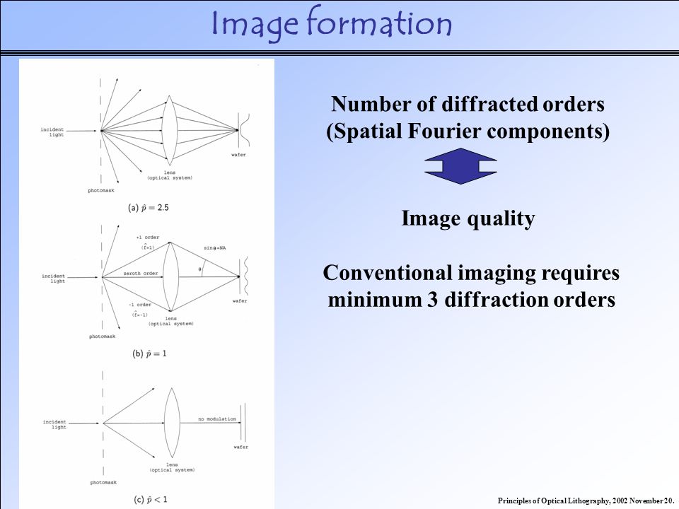
Further reading
- Banqiu Wu and Ajay Kumar (May 2009). Extreme Ultraviolet Lithography. McGraw-Hill Professional, Inc. ISBN 978-0-07-154918-9.
- Banqiu Wu and Ajay Kumar (2009). "Extreme Ultraviolet Lithography: Towards the Next Generation of Integrated Circuits". Optics & Photonics Focus. 7 (4).
Related links
| Main |
| |
|---|---|---|
| Other | ||
| See also | ||