ASML Holding
ASML Holding N.V. is a Dutch company and currently the largest supplier in the world of photolithography systems for the semiconductor industry. The company manufactures machines for the production of integrated circuits. The company is a component of the Euro Stoxx 50 stock market index.[3]
| Naamloze Vennootschap | |
| Traded as |
|
| ISIN | NL0010273215 |
| Industry | Semiconductor industry |
| Founded | 1984 |
| Founder | ASM International, Koninklijke Philips NV |
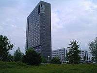
| Headquarters | Veldhoven, Netherlands |
Key people | Peter Wennink (CEO), Gerard Kleisterlee (Chairman of the supervisory board) |
| Products | Photolithography systems for the semiconductor industry |
| Revenue | €10.944 billion (2018)[1] |
| €2.592 billion (2018) | |
| Total assets | €18.196 billion (2017) |
| Total equity | €10.676 billion (2017) |
Number of employees | >23,000 (2019), 123 different nationalities[2] |
| Website | www |
| Footnotes / references >12,000 patents (2019) | |
Products
The photolithography machines manufactured by ASML are used in the production of computer chips. In these machines, patterns are optically imaged onto a silicon wafer that is covered with a film of light-sensitive material (photoresist). This procedure is repeated dozens of times on a single wafer. The photoresist is then further processed to create the actual electronic circuits on the silicon. The optical imaging that ASML's machines deal with is used in the fabrication of nearly all integrated circuits, and as of 2010, ASML has 67 percent of the worldwide sales of lithography machines,[4] with the competition consisting of Ultratech, Canon and Nikon.
Immersion lithography
As of 2011, their high-end TWINSCAN NXT:1950i system is used for producing features down to 32 nanometres (and outlook for 22 nm) at up to 200 wafers per hour,[5] using a water immersion lens and an argon fluoride laser that produces light at a wavelength of 193 nm. As of 2011, an average lithography machine costs 27 million euros.[6]
EUV lithography
ASML manufactures extreme ultraviolet lithography machines that produce light in the 13.3-13.7 nm wavelength range. A high-energy laser is focused on microscopic droplets of molten tin to produce a plasma, which emits EUV light. In 2009, the IMEC research center in Belgium produced the world's first functional 22 nm CMOS SRAM memory cells with a prototype EUV lithography machine.[7] Series-produced (non-prototype) EUV machines were shipped in 2011.[6]
Other
In addition to immersion-based lithography and EUV lithography, ASML has a substantial intellectual property portfolio covering imprint lithography.[8]
Company
ASML's corporate headquarters is in Veldhoven, Netherlands. It is also the location for research, development, manufacturing and assembly. ASML has a worldwide customer base and over sixty service points in sixteen countries. The company is listed on both the AEX and NASDAQ Stock Exchanges, as ASML.
The company (originally named ASM Lithography, current name ASML is an official name and not an abbreviation)[9] was founded in 1984 as a joint venture between the Dutch companies Advanced Semiconductor Materials International (ASMI) and Philips. Nowadays it is a public company with only a minority of the shares owned by Philips.[10] When the company became independent in 1988, it was decided that changing the name was not desirable, and the abbreviation ASML became the official company name.[11] In 2000, ASML acquired the Silicon Valley Group (SVG), a US lithography equipment manufacturer, in a bid to supply 193 nm scanners to Intel Corp.[12][13]
ASML is subject to cyclical industrial dynamics. For example, at the end of 2008, ASML experienced a large drop in sales, which led management to cut the workforce by about 1000 worldwide—mostly contract workers[14]—and to apply for support from the Dutch national unemployment fund to prevent even larger layoffs .[15] Two and a half years later, ASML expected a record-high revenue.[16]
In July 2012, Intel announced a deal to invest $4.1 billion into ASML in exchange for 15% ownership, in order to speed up the transition from 300 mm to 450 mm wafers and further development of EUV lithography.[17][18] This deal is without exclusive rights to future ASML products and, as of July 2012, ASML is offering another 10% of the shares to other companies.[19] As part of their EUV strategy, ASML announced the acquisition of DUV and EUV sources manufacturer Cymer in October 2012.[20] In November 2013, ASML paused development of 450-mm lithography equipment, citing uncertain timing of chipmaker demand.[21] In June 2016, ASML announced their plans to acquire Taiwan-based Hermes Microvision Inc. for about $3.1 billion to add technology for creating smaller and more advanced semiconductors.[22]
References
- https://www.asml.com/press/factsheet/en/s226
- https://d52ahe3agy50c.cloudfront.net/doclib/press/asml_20190208_ASML_Fact_Sheet_FY2018.pdf
- "Frankfurt Stock Exchange". Archived from the original on 8 February 2019. Retrieved 22 October 2015.
- ASML: Sustainability - performance and targets Archived 14 August 2018 at the Wayback Machine. ASML.com (2011)
- ASML Enhances NXT:1950i to Meet Challenging Imaging and Overlay Requirements and Provide a Cost Effective Platform for 22nm. Press release, 12 July 2011.
- Third quarter 2011 results Archived 5 April 2012 at the Wayback Machine. ASML press release.
- IMEC presents functional 22 nm SRAM cells fabricated using EUV technology Archived 1 June 2010 at the Wayback Machine. IMEC press release, 22 April 2009.
- For example, U. S. Patents 7618250, 7692771 and U. S. Patent Applications 20070018360, 20100193994.
- "About ASML: Questions and Answers". ASML Holding. Archived from the original on 28 July 2010. Retrieved 3 August 2010.
- "ASML corporate history". Archived from the original on 1 August 2009. Retrieved 18 December 2008.
- "ASML: About ASML". 20 February 2014. Retrieved 30 November 2014.
- http://www.eetimes.com/document.asp?doc_id=1182430
- http://www.eetimes.com/document.asp?doc_id=1181104
- ASML Takes Action to Adjust Its Organization Due to Severe Order Slowdown Press release.
- Chip-Equipment Firm ASML Cuts Outlook, Sets Layoffs. WSJ.com, 19 December 2008.
- ASML Sees Record Year. Wall Street Journal, April 2011.
- ASML wins funds for chip technology from Intel. Reuters, 10 July 2012.
- ASML Announces Customer Co-Investment Program Aimed at Accelerating Innovation. ASML Press release, 9 July 2012.
- "Intel funds next-gen chipmaking, buys into ASML for $4.1 billion". Reuters. 9 July 2012.
- ASML Press release, 17 October 2012
- "ASML 2013 Annual Report Form (20-F)" (XBRL). United States Securities and Exchange Commission. 11 February 2014.
In November 2013, following our customers’ decision, ASML decided to pause the development of 450mm lithography systems until customer demand and the timing related to such demand is clear.
- Ian King, Bloomberg. “ASML to Acquire Taiwan’s Hermes Microvision for $3.1 Billion.” June 15, 2016. June 16, 2016.
External links
|