Plasmonic nanolithography
Plasmonic nanolithography (also known as plasmonic lithography or plasmonic photolithography)[1] is a nanolithographic process that utilizes surface plasmon excitations such as surface plasmon polaritons (SPPs) to fabricate nanoscale structures. SPPs, which are surface waves that propagate in between planar dielectric-metal layers in the optical regime, can bypass the diffraction limit on the optical resolution that acts as a bottleneck for conventional photolithography.
Theory
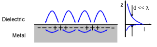
Surface plasmon polaritons are surface electromagnetic waves that propagate in between two surfaces with sign-changing permittivities. They originate from coupling of photons to plasma oscillations, quantized as plasmons. SPPs result in evanescent fields that decay perpendicularly to the interface where the propagation occurs. The dispersion relation for SPPs permits the excitation of wavelengths shorter than the free-space wavelength of the inbound light, additionally ensuring subwavelength field confinement. Nevertheless, the excitation of SPPs necessitate momentum mismatch; prism and grating coupling methods are common.[2] For plasmonic nanolithography processes, this is achieved through surface roughness and perforations.[1]
Methods
Plasmonic contact lithography, a modification on the evanescent near-field lithography, uses a metal photomask, on which the SPPs are excited. Similar to common photolithographic processes, photoresist is exposed to SPPs that propagate from the mask. Photomasks with holes enable grating coupling of SPPs; the fields only propagate for nanometers.[1] Srituravanich et al. has demonstrated the lithographic process experimentally with a 2D silver hole array mask; 90 nm hole arrays were produced at 365 nm wavelength, which is beyond diffraction limit.[3] Zayats and Smolyaninov utilized a multi-layered metal film mask to enhance the subwavelength aperture; such structures can be realized by thin film deposition methods. Bowtie apertures and nanogaps were also suggested as alternative apertures.[1] A version of the method, named as surface plasmon interference nanolithography by Liu et al., uses SPP interference patterns.[4] Despite offering high resolution and throughput, plasmonic contact lithography is regarded as an expensive and complex method; contamination due to contact is also a limiting factor.[1]
Planar lens imaging nanolithography uses plasmonic lenses or negative-index superlenses, which were first proposed by Pendry. Many superlens designs, such as Pendry's thin silver film or Fang et al.'s superlens, benefit from plasmonic excitations to focus Fourier components of incoming light beyond the diffraction limit.[1] Chaturvedi et al. has demonstrated the imaging of a 30 nm chromium grating through silver superlens photolithography at 380 nm,[5] while Shi et al. simulated a 20 nm lithography resolution at 193 nm wavelength with an aluminum superlens.[6] Srituravanich et al. has developed a mechanically adjustable, hovering plasmonic lens for maskless near-field nanolithography,[7] whereas another maskless approach by Pan et al. uses a "multi-stage plasmonic lens" for progressive coupling.[8]
Plasmonic direct writing is a maskless form of photolithography that is based on scanning probe lithography; the method uses localized surface plasmon (LSP) enhancements from embedded plasmonic scanning probes to expose the photoresist.[1][9] Wang et al. experimentally demonstrated 100 nm field confinement with this method.[10] Kim et al. has developed a ~50 nm resolution scanning probe with a patterning speed of ~10 mm/s.[11]
See also
References
- Xie, Zhihua; Yu, Weixing; Wang, Taisheng; et al. (31 May 2011). "Plasmonic nanolithography: a review". Plasmonics. 6 (3): 565–580. doi:10.1007/s11468-011-9237-0.
- Maradudin, Alexei A.; Sambles, J. Roy; Barnes, William L., eds. (2014). Modern Plasmonics. Amsterdam: Elsevier. p. 1–23. ISBN 9780444595263.
- Srituravanich, Werayut; Fang, Nicholas; Sun, Cheng; et al. (2004). "Plasmonic nanolithography". Nano Letters. 4 (6): 1085–1088. Bibcode:2004NanoL...4.1085S. doi:10.1021/nl049573q.
- Liu, Zhao-Wei; Wei, Qi-Huo; Zhang, Xiang (2005). "Surface plasmon interference nanolithography". Nano Letters. 5 (5): 957–961. Bibcode:2005NanoL...5..957L. doi:10.1021/nl0506094. PMID 15884902.
- Chaturvedi1, Pratik; Wu, Wei; Logeeswaran, VJ; et al. (25 January 2010). "A smooth optical superlens". Applied Physics Letters. 96 (4): 043102. Bibcode:2010ApPhL..96d3102C. doi:10.1063/1.3293448.
- Shi, Zhong; Kochergin, Vladimir; Wang, Fei (2009). "193nm superlens imaging structure for 20nm lithography node". Optics Express. 17 (3): 11309–11314. Bibcode:2009OExpr..1711309S. doi:10.1364/OE.17.011309. PMID 19582044.
- Srituravanich, Werayut; Pan, Liang; Wang, Yuan; Sun, Cheng (12 October 2008). "Flying plasmonic lens in the near field for high-speed nanolithography". Nature Nanotechnology. 3 (12): 733–737. Bibcode:2008NatNa...3..733S. doi:10.1038/nnano.2008.303. PMID 19057593.
- Pan, Liang; Park, Yongshik; Xiong, Yi; Ulin-Avila, Erick (29 November 2011). "Maskless plasmonic lithography at 22 nm resolution". Scientific Reports. 1 (175). doi:10.1038/srep00175. PMID 22355690.
- Heltzel, Alex; Theppakuttai, Senthil; Chen, S.C.; Howell, John R. (6 December 2007). "Surface plasmon-based nanopatterning assisted by gold nanospheres". Nanotechnology. 19 (2): 025305. doi:10.1088/0957-4484/19/02/025305. PMID 21817542.
- Wang, Yuan; Srituravanich, Werayut; Sun, Cheng; Zhang, Xiang (2008). "Plasmonic nearfield scanning probe with high transmission". Nano Letters. 8 (9): 3041–3045. Bibcode:2008NanoL...8.3041W. CiteSeerX 10.1.1.862.5284. doi:10.1021/nl8023824. PMID 18720976.
- Kim, Yongwoo; Kim, Seok; Jung, Howon; et al. (2009). "Plasmonic nano lithography with a high scan speed contact probe". Optics Express. 17 (22): 19476–19485. Bibcode:2009OExpr..1719476K. doi:10.1364/OE.17.019476. PMID 19997168.
| Main |
| |
|---|---|---|
| Other | ||
| See also | ||