Multiple patterning
Multiple patterning (or multi-patterning) is a class of technologies for manufacturing integrated circuits (ICs), developed for photolithography to enhance the feature density. It is expected to be necessary for the upcoming 10 nm and 7 nm node semiconductor processes and beyond. The premise is that a single lithographic exposure may not be enough to provide sufficient resolution. Hence additional exposures would be needed, or else positioning patterns using etched feature sidewalls (using spacers) would be necessary.
Even for electron-beam lithography, single exposure appears insufficient at ≈10 nm half-pitch, hence requiring double patterning.[1][2]
Situations Requiring Multiple Patterning
There are a number of situations which lead to multiple patterning being required.
Sub-Resolution Pitch
The most obvious case requiring multiple patterning is when the feature pitch is below the resolution limit of the optical projection system. For a system with numerical aperture NA and wavelength λ, any pitch below 0.5 λ/NA would not be resolvable in a single wafer exposure.
Different Parts of Layout Requiring Different Illuminations

When patterns include feature sizes near the resolution limit, it is common that different arrangements of such features will require specific illuminations for them to be printed.
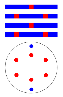
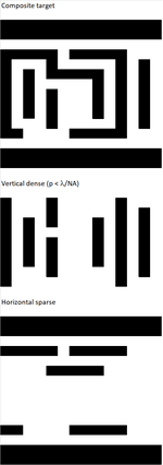
The most basic example is horizontal dense lines vs. vertical lines (half-pitch < 0.35 λ/NA), where the former requires a North-South dipole illumination while the latter requires an East-West dipole illumination. If both types are used (also known as cross-quadrupole C-Quad), the inappropriate dipole degrades the image of the respective line orientation.[3]
In DRAM, the array and periphery are exposed at different illumination conditions. For example, the array could be exposed with dipole illumination while the periphery could use annular illumination.[4] This situation applies to any set of patterns (half-pitch < 0.5 λ/NA) with different pitches or different feature arrangements, e.g., rectangular arrays vs. staggered arrays.[5] Any of the individual patterns is resolvable, but a single illumination cannot be used simultaneously for all of them.
The inclusion of both isolated and dense features is a well-known instance of multi-pitch patterning. Subresolution assist features (SRAFs) have been designed to enable the patterning of isolated features when using illumination tailored for the dense features. However, not all pitch ranges can be covered. In particular, semi-dense features may not be included.[6]
Multi-Pitch Patterns
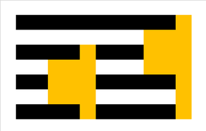
Sometimes a feature pattern inherently contains more than one pitch, and furthermore, these pitches are incompatible to the extent that no illumination can simultaneously image both pitches satisfactorily. A common example, again from DRAM, is the brick pattern defining the active regions of the array.[7] In addition to the narrow pitch of the active regions, there is also the pitch between the active region separations or breaks, which is double that of the narrow pitch in the same direction. When the narrow pitch is < λ/NA (but still > 0.5 λ/NA), it cannot be imaged simultaneously with the double pitch due to the focus limitations of the latter.
Small deviations from 2-beam interference
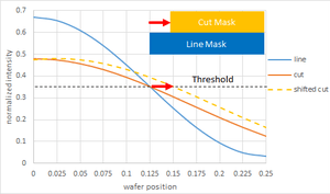
A two-beam interference pattern (half-pitch <0.5 λ/NA) forms a set of regularly spaced lines. Breaks in such lines are deviations from the interference pattern. Such breaks generally do not dominate the pattern, and are thus small deviations. These deviations are insufficient to completely offset the constructive or destructive interference of the underlying regular line pattern; sidelobes often result.[8][9] Another mask exposure (usually referred as a cut mask) is therefore necessary to break the line pattern more robustly.
Line Cutting

The earliest implementation of multiple patterning involved line cutting. This first occurred for Intel's 45nm node, for 160 nm gate pitch.[10] The use of a second mask to cut lines defined by a first mask does not help increase feature density directly. Instead it allows definition of features, e.g., brick patterns, which are based on lines spaced at a minimum pitch, in particular, when the lines are near the resolution limit and are generated by the two-beam interference mentioned above. The two-beam interference still dominates the diffraction pattern.[8]
When applying the second mask to cut lines, the overlay relative to the first mask needs to be considered; otherwise, edge placement errors (EPE) may result. The cut pitch can be 1.4-2 times the pitch of the lines to be cut. If the line pitch is already near the resolution limit, the cut pattern itself may have imaging difficulty, from reduced dose or focus window. In this case, more than one cut mask would have to be used. However, the use of a cut mask adds the risk of feature damage from an overlay error. Self-aligned cutting (to be discussed below) may be a preferred option.
Pitch Splitting

The earliest form of multiple patterning involved simply dividing a pattern into two or three parts, each of which may be processed conventionally, with the entire pattern combined at the end in the final layer. This is sometimes called pitch splitting, since two features separated by one pitch cannot be imaged, so only skipped features can be imaged at once. It is also named more directly as "LELE" (Litho-Etch-Litho-Etch). This approach has been used for the 20 nm and 14 nm nodes. The additional cost of extra exposures was tolerated since only a few critical layers would need them. A more serious concern was the effect of feature-to-feature positioning errors (overlay). Consequently, the self-aligned sidewall imaging approach (described below) has succeeded this approach.
A "brute force" approach for patterning trenches involves a sequence of (at least) two separate exposures and etchings of independent patterns into the same layer. For each exposure, a different photoresist coating is required. When the sequence is completed, the pattern is a composite of the previously etched subpatterns. By interleaving the subpatterns, the pattern density can theoretically be increased indefinitely, the half-pitch being inversely proportional to the number of subpatterns used. For example, a 25 nm half-pitch pattern can be generated from interleaving two 50 nm half-pitch patterns, three 75 nm half-pitch patterns, or four 100 nm half-pitch patterns. The feature size reduction will most likely require the assistance of techniques such as chemical shrinks, thermal reflow, or shrink assist films. This composite pattern can then be transferred down into the final layer.
This is best described by considering a process example. A first exposure of photoresist is transferred to an underlying hardmask layer. After the photoresist is removed following the hardmask pattern transfer, a second layer of photoresist is coated onto the sample and this layer undergoes a second exposure, imaging features in between the features patterned in the hardmask layer. The surface pattern is made up of photoresist features edged between mask features, which can be transferred into the final layer underneath. This allows a doubling of feature density.
A variation on this approach which eliminates the first hardmask etch is resist freezing,[11] which allows a second resist coating over the first developed resist layer. JSR has demonstrated 32 nm lines and spaces using this method,[12] where the freezing is accomplished by surface hardening of the first resist layer.
In recent years, the scope of the term 'pitch splitting' has gradually been expanded to include techniques involving sidewall spacers.
Sidewall Image Transfer
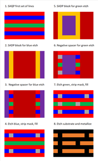
In spacer patterning, a spacer is a film layer formed on the sidewall of a pre-patterned feature. A spacer is formed by deposition or reaction of the film on the previous pattern, followed by etching to remove all the film material on the horizontal surfaces, leaving only the material on the sidewalls. By removing the original patterned feature, only the spacer is left. However, since there are two spacers for every line, the line density has now doubled. This is commonly referred to as Self-Aligned Double Patterning (SADP). The spacer technique is applicable for defining narrow gates at half the original lithographic pitch, for example.
As pitch splitting has become more difficult due to possible differences in feature positions between different exposed parts, sidewall image transfer (SIT) has become more recognized as the necessary approach. The SIT approach typically requires a spacer layer to be formed on an etched feature's sidewall. If this spacer corresponds to a conducting feature, then ultimately it must be cut at no less than two locations to separate the feature into two or more conducting lines as typically expected. On the other hand, if the spacer corresponds to a dielectric feature, cutting would not be necessary. The prediction of how many cuts would be needed for advanced logic patterns has been a large technical challenge. Many approaches for spacer patterning have been published (some listed below), all targeting the improved management (and reduction) of the cuts.
As spacer materials are commonly hardmask materials, their post-etch pattern quality tends to be superior compared to photoresist profiles after etch, which are generally plagued by line edge roughness.[13]
The main issues with the spacer approach are whether the spacers can stay in place after the material to which they are attached is removed, whether the spacer profile is acceptable, and whether the underlying material is attacked by the etch removing the material attached to the spacer. Pattern transfer is complicated by the situation where removal of the material adjacent to the spacers also removes a little of the underlying material. This results in higher topography on one side of the spacer than the other.[14] Any misalignment of masks or excursion in pre-patterned feature critical dimension (CD) will cause the pitch between features to alternate, a phenomenon known as pitch walking.[15]
The positioning of the spacer also depends on the pattern to which the spacer is attached. If the pattern is too wide or too narrow, the spacer position is affected. However, this would not be a concern for critical memory feature fabrication processes which are self-aligned.
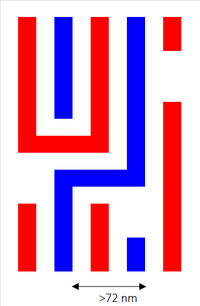
When SADP is repeated, an additional halving of the pitch is achieved. This is often referred to as Self-Aligned Quadruple Patterning (SAQP). With 76 nm being the expected minimum pitch for a single immersion lithography exposure,[16] 19 nm pitch is now accessible with SAQP.
Self-aligned contact/via patterning

Self-aligned contact and via patterning is an established method for patterning multiple contacts or vias from a single lithographic feature. It makes use of the intersection of an enlarged feature resist mask and underlying trenches which are surrounded by a pre-patterned hardmask layer. This technique is used in DRAM cells[17] and is also used for advanced logic to avoid multiple exposures of pitch-splitting contacts and vias.[18][19][20]
Since 32 nm node, Intel has applied the above-mentioned self-aligned via approach, which allows two vias separated by a small enough pitch (112.5 nm for Intel 32 nm metal)[21] to be patterned with one resist opening instead of two separate ones.[20] If the vias were separated by less than the single exposure pitch resolution limit, the minimum required number of masks would be reduced, as two separate masks for the originally separated via pair can now be replaced by a single mask for the same pair.
Spacer-is-Dielectric (SID) SADP

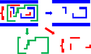
In self-aligned double patterning (SADP), the number of cut/block masks may be reduced or even eliminated in dense patches when the spacer is used to directly pattern inter-metal dielectric instead of metal features.[22] The reason is the cut/block locations in the core/mandrel features are already patterned in the first mask. There are secondary features which emerge from the gaps between spacers after further patterning. The edge between a secondary feature and the spacer is self-aligned with the neighboring core feature.
2D SID Spacer Patterning
The use of SID may be applied to 2D arrays, by iteratively adding features equidistant from the previously present features, doubling the density with each iteration.[23][24] Cuts not requiring tight positioning may be made on this spacer-generated grid.[25]
Triangular Spacer (Honeycomb Structure) Patterning

Samsung recently demonstrated DRAM patterning using a honeycomb structure (HCS) suitable for 20 nm and beyond.[26] Each iteration of spacer patterning triples the density, effectively reducing 2D pitch by a factor of sqrt(3). This is particularly useful for DRAM since the capacitor layer can be fit to a honeycomb structure, making its patterning simpler.
Directed Self-Assembly (DSA)
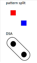
The number of masks used for sidewall spacer patterning may be reduced with the use of directed self-assembly (DSA) due to the provision of gridded cuts all at once within a printed area, which can then be selected with a final exposure.[27][25] Alternatively, the cut pattern itself may be generated as a DSA step.[28] Likewise, a split via layout may be recombined in pairs.[29]
Much progress had been reported on the use of PMMA-PS block copolymers to define sub-20 nm patterns by means of self-assembly, guided by surface topography (graphoepitaxy) and/or surface chemical patterning (chemoepitaxy).[30] The key benefit is the relatively simple processing, compared to multiple exposures or multiple depositions and etching. The main drawback of this technique is the relatively limited range of feature sizes and duty cycles for a given process formulation. Typical applications have been regular lines and spaces as well as arrays of closely packed holes or cylinders.[31] However, random, aperiodic patterns may also be generated using carefully defined guiding patterns.[32]
The line edge roughness in block copolymer patterns is strongly dependent on the interface tension between the two phases, which in turn, depends on the Flory "chi" (χ) parameter.[33] A higher value of χ is preferred for reduced roughness; the interfacial width between domains is equal to 2a(6χ)−1/2, where a is the statistical polymer chain length.[34] Moreover, χN > 10.5 is required for sufficient phase segregation, where N is the degree of polymerization (number of monomer repeats in the chain). On the other hand, the half-pitch is equal to 2(3/π2)1/3aN2/3χ1/6. The fluctuations of the pattern widths are actually only weakly (square root) dependent on the logarithm of the half-pitch, so they become more significant relative to smaller half-pitches.
DSA has not yet been implemented in manufacturing, due to defect concerns, where a feature does not appear as expected by the guided self-assembly.[35]
Other multi-patterning techniques
There have been numerous concerns that multiple patterning diminishes or even reverses the node-to-node cost reduction expected with Moore's Law. EUV is more expensive than three 193i exposures (i.e., LELELE), considering the throughput.[36] Moreover, EUV is more liable to print smaller mask defects not resolvable by 193i.[37] Some aspects of other considered multi-patterning techniques are discussed below.
Self-Aligned Triple Patterning (SATP)
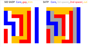
Self-aligned triple patterning has been considered as a promising successor to SADP, due to its introduction of a second spacer offering additional 2D patterning flexibility and higher density.[38][39] A total of two masks (mandrel and trim) is sufficient for this approach.[40] The only added cost relative to SADP is that of depositing and etching the second spacer. The main disadvantage of SATP succeeding SADP is that it would only be usable for one node. For this reason, self-aligned quadruple patterning (SAQP) is more often considered. On the other hand, the conventional SID SADP flow may be extended quite naturally to triple patterning, with the second mask dividing the gap into two features.[41]
Tilted Ion Implantation
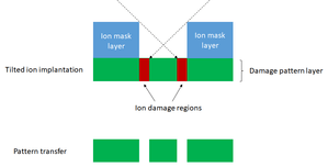
Tilted ion implantation was proposed in 2016 by the University of Berkeley as an alternative method of achieving the same result as spacer patterning.[42] Instead of core or mandrel patterns supporting deposited spacers, an ion masking layer pattern shields an underlying layer from being damaged by ion implantation, which leads to being etched away in a subsequent process. The process requires the use of angled ion beams which penetrate to just the right depth, so as not to damage already processed layers underneath. Also, the ion masking layer must behave ideally, i.e., blocking all ions from passing through, while also not reflecting off the sidewall. The latter phenomenon would be detrimental and defeat the purpose of the ion masking approach. Trenches as small as 9 nm have been achieved with this approach, using 15 keV Ar+ ion implantation at 15-degree angles into a 10 nm thermal SiO2 masking layer. A fundamental aspect of this approach is the correlation between damage width and damage pitch; both widen at the same time for fixed ion mask height and ion beam angle.
Complementary polarity exposures
The method of complementary exposures[43] is another way of reducing mask exposures for multiple patterning. Instead of multiple mask exposures for individual vias, cuts or blocks, two exposures of opposing or complementary polarity are used, so that one exposure removes interior portions of the previous exposure pattern. The overlapped regions of two polygons of opposite polarity do not print, while the non-overlapped regions define locations that print according to the polarity. Neither exposure patterns the target features directly. This approach was also implemented by IMEC as two "keep" masks for the M0A layer in their 7nm SRAM cell.[44]
Self-Aligned Blocking or Cutting
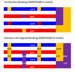
Self-aligned blocking or cutting is currently being targeted for use with SAQP for sub-30 nm pitches.[45] The lines to be cut are divided into two materials, which can be etched selectively. One cut mask only cuts every other line made of one material, while the other cut mask cuts the remaining lines made of the other material.
EUV Multiple Patterning Possibilities
Although EUV has been projected to be the next-generation lithography of choice, it could still require more than one lithographic exposure, due to the foreseen need to first print a series of lines and then cut them; a single EUV exposure pattern has difficulty with line end-to-end spacing control.[46]
The existing 0.33 NA EUV tools are challenged below 16 nm half-pitch resolution.[47] Tip-to-tip gaps are problematic for 16 nm dimensions.[48] Consequently, EUV 2D patterning is limited to >32 nm pitch.[47] Recent studies of optimizing the EUV mask features and the illumination shape simultaneously have indicated that different patterns in the same metal layer could require different illuminations.[49][50][51][52][53] On the other hand, a single exposure only offers a single illumination.
For example, in a cross-pitch source-mask optimization for 7nm node, for 40-48 nm pitch and 32 nm pitch, the quality as determined by the normalized image log slope was insufficient (NILS<2), while only 36 nm pitch was barely satisfactory for bidirectional single exposure.[54]
The underlying situation is that EUV patterns may be split according to different illuminations for different pitches, or different pattern types (e.g., staggered arrays vs. regular arrays).[49] This could apply to line-cutting patterns as well as contact/via layers. It is also likely more than one cut would be needed, even for EUV.[55]
At the 2016 EUVL Workshop, ASML reported that the 0.33 NA NXE EUV tools would not be capable of standard single exposure patterning for the 11-13 nm half-pitch expected at the 5 nm node.[56] A higher NA of 0.55 would allow single exposure EUV patterning of fields which are half the 26 mm x 33 mm standard field size.[56] However, some products, such as NVIDIA's Pascal Tesla P100,[57] will be bisected by the half-field size, and therefore require stitching of two separate exposures.[58] In any case, two half-field scans consume twice as much acceleration/deceleration overhead as a single full-field scan.[56][59]
Multipatterning Implementations
Memory patterns are already patterned by quadruple patterning for NAND[60] and crossed quadruple/double patterning for DRAM.[61] These patterning techniques are self-aligned and do not require custom cutting or trim masks. For 2x-nm DRAM and flash, double patterning techniques should be sufficient.
Current EUV throughput is still more than 3x slower than 193 nm immersion lithography, thus allowing the latter to be extended by multiple patterning. Furthermore, the lack of an EUV pellicle is also prohibitive.
As of 2016, Intel was using SADP for its 10 nm node;[62] however, as of 2017, the 36 nm minimum metal pitch is now being achieved by SAQP.[63] Intel is using triple patterning for some critical layers at its 14 nm node,[64] which is the LELELE approach.[65] Triple patterning is already demonstrated in 10 nm tapeout,[66] and is already an integral part of Samsung's 10 nm process.[67] TSMC is deploying 7 nm in 2017 with multiple patterning;[68] specifically, pitch-splitting,[69] down to 40 nm pitch.[70] Beyond the 5 nm node, multiple patterning, even with EUV assistance, would be economically challenging, since the departure from EUV single exposure would drive up the cost even higher. However, at least down to 12 nm half-pitch, LELE followed by SADP (SID) appears to be a promising approach, using only two masks, and also using the most mature double patterning techniques, LELE and SADP.[71]
Patterning Costs

| Patterning Method | Normalized Wafer Cost |
|---|---|
| 193i SE | 1 |
| 193i LELE | 2.5 |
| 193i LELELE | 3.5 |
| 193i SADP | 2 |
| 193i SAQP | 3 |
| EUV SE | 4 |
| EUV SADP | 6 |
Ref.: A. Raley et al., Proc. SPIE 9782, 97820F (2016).
Compared to 193i SADP, EUV SADP cost is dominated by the EUV tool exposure, while the 193i SAQP cost difference is from the added depositions and etches. The processing cost and yield loss at a lithographic tool is expected to be highest in the whole integrated process flow due to the need to move the wafer to specific locations at high speed. EUV further suffers from the shot noise limit, which forces the dose to increase going for successive nodes.[72] On the other hand, depositions and etches process entire wafers at once, without the need for wafer stage motion in the process chamber. In fact, multiple layers may be added under the resist layer for anti-reflection or etch hard-mask purposes, just for conventional single exposure.
Multi-Patterning Practices
| Company | Logic Process | Minimum Metal Pitch (MMP) | Contacted Gate Pitch (CGP) | Fin Pitch | MMP Patterning Technique | Production Start |
|---|---|---|---|---|---|---|
| Intel | 14nm | 52 nm[73] | 70 nm[73] | 42 nm[73] | SADP[73] | 2014[73] |
| Intel | 10nm | 36 nm[63] | 54 nm[63] | 34 nm[63] | SAQP[63][74] | end of 2018[75] |
| TSMC | 16FF | 64 nm[76] | 90 nm[76] | 48 nm[76] | LELE[77] | 2015[76] |
| TSMC | 10FF | 42 nm[78] | 64 nm[78] | 36 nm[78] | SADP[79] | 2017[78] |
| TSMC | 7FF | 40 nm[70] | 57 nm[80] | SADP[79] | early 2017[81] | |
| Samsung | 14LP* | 64 nm[73] | 78 nm[73] | 48 nm[73] | LELE[73] | 2015[73] |
| Samsung | 10LPE | 48 nm[82] | 64 nm[82] | LELELE[67] | end of 2016[67] | |
| Samsung | 8LPP | 44 nm[83] | 64 nm[83] | LELELELE[83] | end of 2018 | |
| GlobalFoundries | 7LP | 40 nm[80] | 56 nm[80] | 30 nm[84] | SADP[80] | 2018[85] |
Mask Costs
The mask cost strongly benefits from the use of multiple patterning. The EUV single exposure mask has smaller features which take much longer to write than the immersion mask. Even though mask features are 4x larger than wafer features, the number of shots is exponentially increased for much smaller features. Furthermore, the sub-100 nm features on the mask are also much harder to pattern, with absorber heights ≈70 nm.[86]
Wafer Productivity
| Tool | EUV | EUV | Immersion | Immersion |
|---|---|---|---|---|
| WPH (wafers per hour) | 85 | 85 | 275 | 275 |
| # tools | 6 | 6 | 24[87] | 24 |
| uptime | 70% | 70% | 90% | 90% |
| # passes | 1 | 2 | 2 | 4 |
| WPM (wafers per month) | 257,040 | 128,520 | 2,138,400 | 1,069,200 |
| normalized WPM | 1 | 0.5 | 8 | 4 |
Note: WPM = WPH * # tools * uptime / # passes * 24 hrs/day * 30 days/month. Normalized WPM = WPM/(WPM for EUV 1 pass)
Multiple patterning with immersion scanners can be expected to have higher wafer productivity than EUV, even with as many as 4 passes per layer, due to faster wafer exposure throughput (WPH), a larger number of tools being available, and higher uptime.
Multiple Patterning Specific Issues
| Issue | LELE | LELELE | SID SADP | SAQP |
|---|---|---|---|---|
| Overlay | between 1st and 2nd exposures, especially where stitching | among all three exposures, especially where stitching | between core and cut exposures | between core and cut exposures |
| Exposed feature width | (1) 1st exposure (2) 2nd exposure | (1) 1st exposure (2) 2nd exposure (3) 3rd exposure | core feature | (1) core feature (2) cut shape |
| Feature slimming target width | 1/4 exposure pitch | 1/6 exposure pitch | 1/4 core pitch | 1/8 core pitch |
| Spacer width | N/A | N/A | 1 spacer | (1) 1st spacer (2) 2nd spacer |
Multiple patterning entails the use of many processing steps to form a patterned layer, where conventionally only one lithographic exposure, one deposition sequence and one etch sequence would be sufficient. Consequently, there are more sources of variations and possible yield loss in multiple patterning. Where more than one exposure is involved, e.g., LELE or cut exposures for SAQP, the alignment between the exposures must be sufficiently tight. Current overlay capabilities are ≈0.6 nm for exposures of equal density (e.g., LELE) and ≈2.0 nm for dense lines vs. cuts/vias (e.g., SADP or SAQP) on dedicated or matched tools.[88] In addition, each exposure must still meet specified width targets. Where spacers are involved, the width of the spacer is dependent on the initial deposition as well as the subsequent etching duration. Where more than one spacer is involved, each spacer may introduce its own width variation.
Mixed patterning methods
Multiple patterning may evolve toward a combination of multiple exposures, spacer patterning, and/or EUV. Especially with tip-to-tip scaling being difficult in a single exposure on current EUV tools,[46] a line-cutting approach may be necessary.
| Lines | Grid intersecting lines | Selected grid locations for cuts/vias |
|---|---|---|
| a. EUV exposure; b. SADP/SAQP; c. multiple DUV exposures | a. EUV 2nd exposure; b. overlaid spacer grid (DUV 2nd exposure);[89][90] c. multiple DUV exposures or two self-aligned blocking DUV exposures | a. (included in EUV 2nd exposure); b. overlaid spacer grid location selection (DUV 3rd exposure);[89][90][43] c. (included in multiple DUV exposures or self-aligned blocking) |
For line patterning, SADP/SAQP could have the advantage over the EUV exposure, due to cost and maturity of the former approach and stochastic missing or bridging feature issues of the latter.[91] For grid location patterning, a single DUV exposure following grid formation also has the cost and maturity advantages (e.g., immersion lithography may not even be necessary for the spacer patterning in some cases) and no stochastic concerns associated with EUV. Grid location selection has an advantage over direct point cutting because the latter is sensitive to overlay and stochastic edge placement errors, which may distort the line ends.[92]
Industrial Adoption
The evolution of multiple patterning is being considered in parallel with the emergence of EUV lithography. While EUV lithography satisfies 10-20 nm resolution by basic optical considerations, the occurrence of stochastic defects[93] as well as other infrastructure gaps and throughput considerations prevent its adoption currently. Consequently, 7nm tapeouts have largely proceeded without EUV.[94] In other words, the multiple patterning is not prohibitive, but more like a nuisance and growing expense. 5nm may be expected in 2020, with the evolution of multiple patterning and status of EUV considered at that time.
7nm and 5nm FinFETs
Self-aligned quadruple patterning is already the established process to be used for patterning fins for 7 nm and 5 nm FinFETs.[95] With SAQP, each patterning step gives a critical dimension uniformity (CDU) value in the sub-nanometer range (3 sigma). Among the four logic/foundry manufacturers, only Intel is applying SAQP to the metal layers, as of 2017.[74]
DRAM
Like NAND Flash, DRAM has also made regular use of multiple patterning. Even though the active areas form a two-dimensional array, one cut mask is sufficient for 20 nm.[96] Furthermore, the cut mask may be simultaneously used for patterning the periphery, and thus would not count as an extra mask.[97] However, for 14-18 nm, one additional cut mask would be necessary for dividing the active areas. Samsung has already started manufacturing the 18 nm DRAM.[98]
3D NAND Flash
3D NAND flash may use SADP for some layers. While it does not scale so aggressively laterally, the use of string stacking in 3D NAND would imply the use of multiple patterning (litho-etch style) to pattern the vertical channels.
References
- ↑ Chao, Weilun; Kim, Jihoon; Anderson, Erik H.; Fischer, Peter; Rekawa, Senajith; Attwood, David T. (2009-01-09). "Double patterning HSQ processes of zone plates for 10 nm diffraction limited performance".
- ↑ Duan, Huigao; Winston, Donald; Yang, Joel K. W.; Cord, Bryan M.; Manfrinato, Vitor R.; Berggren, Karl K. (November 2010). "Sub-10-nm half-pitch electron-beam lithography by using poly(methyl methacrylate) as a negative resist" (PDF). Journal of Vacuum Science & Technology B, Nanotechnology and Microelectronics: Materials, Processing, Measurement, and Phenomena. 28 (6): C6C58–C6C62. doi:10.1116/1.3501353. Archived from the original (PDF) on 2012-01-19.
- ↑ M. Burkhardt et al., Proc. SPIE 6520, 65200K (2007).
- ↑ T. Winkler et al., Proc. SPIE 5754, 1169 (2005).
- ↑ Y. Chen et al., J. Vac. Sci. & Tech. B 35, 06G601 (2017).
- ↑ F. M. Schellenberg et al., DAC 2001,Adoption of OPC and the Impact on Design and Layout.
- ↑ Samsung 80nm DRAM
- 1 2 N. Singh and M. Mukherjee-Roy, Proc. SPIE vol. 4691, 1054 (2002).
- ↑ J. Garofalo et al., J. Vac. Sci. & Tech. B 11, 2651 (1993).
- ↑ Intel Technology Journal 45nm issue
- ↑ "Scaling-driven nanoelectronics - Resists". Archived from the original on 2010-03-23.
- ↑ LaPedus, Mark (March 13, 2008). "JSR demos 'freezing material' for 22-nm production". Archived from the original on 2014-07-15.
- ↑ X. Hua et al., J. Vac. Sci. Tech. B, vol. 24, pp. 1850-1858 (2006).
- ↑ Y-K Choi et al., J. Phys. Chem. B, vol. 107, pp. 3340-3343 (2003).
- ↑ Chao, Robin; Kohli, Kriti K.; Zhang, Yunlin; Madan, Anita; Muthinti, Gangadhara Raja; Hong, Augustin J.; Conklin, David; Holt, Judson; Bailey, Todd C. (2014-01-01). "Multitechnique metrology methods for evaluating pitch walking in 14 nm and beyond FinFETs". Journal of Micro/Nanolithography, MEMS, and MOEMS. 13 (4): 041411–041411. doi:10.1117/1.JMM.13.4.041411. ISSN 1932-5150.
- ↑ I. Bouchoms et al., Proc. SPIE 7274, 72741K (2009).
- ↑ US Patent 6165880, assigned to TSMC.
- ↑ Y. Loquet et al., Microelec. Eng. 107, 138 (2013).
- ↑ US Patent 8813012, assigned to Synopsys.
- 1 2 R. Brain et al., IITC 2009.
- ↑ P. Packan et al., IEDM 2009.
- ↑ Ref.: US Patent 8312394, assigned to Synopsys.
- ↑ K. Oyama et al., Proc. SPIE 9051, 90510V (2014).
- ↑ B. Mebarki et al., U. S. Patent 8,084,310, assigned to Applied Materials.
- 1 2 M. C. Smayling et al., Proc. SPIE 8683, 868305 (2013).
- ↑ J. M. Park et al., IEDM 2015, 676 (2015).
- ↑ Synopsis Presentation at Semicon West 2013 Archived 2015-09-24 at the Wayback Machine.
- ↑ Z. Xiao et al., Proc. SPIE 8880, 888017-3 (2013).
- ↑ J. Bekaert et al., Proc. SPIE 9658, 965804 (2015).
- ↑ S. H. Park et al., Soft Matter, 6, 120-125 (2010).
- ↑ C. G. Hardy and C. Tang, J. Polymer Sci. Pt. B: Polymer Phys., vol. 51, pp. 2-15 (2013).
- ↑ L-W. Chang et al.IEDM 2010 Technical Digest, 752-755 (2010).
- ↑ NIST 2011 report on LER in PS-b-PMMA DSA
- ↑ A. N. Semenov, Macromolecules 26, 6617 (1993).
- ↑ A. Gharbi et al., Proc. SPIE 9777, 97770T (2016).
- ↑ D. Civay et al., J. Micro/Nanolith. MEMS MOEMS 14, 023501 (2015).
- ↑ K. Seki et al., Proc. SPIE 9658, 96580G (2015).
- ↑ US Patent 7842601, assigned to Samsung.
- ↑ Y. Chen et al., Proc. SPIE 7973, 79731P (2011).
- ↑ M. Mirsaeedi et al., IEEE Trans. VLSI Syst. 22, 1170 (2014).
- ↑ US Patent 7846849, assigned to Applied Materials.
- ↑ S. W. Kim et al., JVST B 34, 040608 (2016).
- 1 2 F. T. Chen et al., Proc. SPIE 8326, 83262L (2012).
- ↑ S. Sakhare et al., Proc. SPIE 9427, 94270O (2015).
- ↑ N. Mohanty et al., Proc. SPIE 10147, 1014704 (2017).
- 1 2 van Setten, Eelco; Wittebrood, Friso; et al. (September 4, 2015). "Patterning options for N7 logic: prospects and challenges for EUV". Proc. SPIE 9661, 31st European Mask and Lithography Conference, 96610G. doi:10.1117/12.2196426.
- 1 2 T-B. Chiou et al., Proc. SPIE 9781, 978107 (2016).
- ↑ T. H-Bao et al., Proc. SPIE 9781, 978102 (2016).
- 1 2 Y. Chen et al., J. Vac. Sci. Tech. B35, 06G601 (2017).
- ↑ M. Crouse et al., Proc. SPIE 10148, 101480H (2017).
- ↑ W. Gillijns et al., Proc. SPIE 10143, 1014314 (2017).
- ↑ T. Last et al., Proc. SPIE 10143, 1014311 (2017).
- ↑ S. Hsu et al., Proc. SPIE 9422, 94221I (2015).
- ↑ R-H. Kim et al., Proc. SPIE vol. 9776, 97761R (2016).
- ↑ Merritt, Rick (October 7, 2015). "5nm Test Lights Litho Path Hybrid 193i, EUV seen as best approach". EETimes.
- 1 2 3 ASML High-NA EUV
- ↑ NVIDIA Pascal Tesla P100 Unveiled - 15.3 Billion Transistors on a 610mm2 16nm Die
- ↑ Microlithography: Science and Technology, 2nd ed., B. W. Smith and K. Suzuki (eds.), CRC Press, 2007, p. 94.
- ↑ Handbook of Semiconductor Manufacturing Technology, Y. Nishi and R. Doering (eds.), CRC Press, 2000, p. 475.
- ↑ Hynix M1X NAND
- ↑ U.S. Patent 9318369, assigned to Samsung.
- ↑ Intel discusses 10nm
- 1 2 3 4 5 Intel unveils 10nm
- ↑ Intel goes to 7nm without EUV
- ↑
- ↑ Triple patterning is becoming common at 10nm
- 1 2 3 Samsung announces 10nm FinFET process for SoC
- ↑
- ↑ S. Y. Wu et al., IEDM 2016, paper 2.7.
- 1 2 IEDM 2016 Setting Stage for 7/5 nm
- ↑ F. T. Chen et al., Proc. SPIE 8683, 868311 (2013).
- ↑ F. T. Chen et al., Proc. SPIE vol. 8326, 82362L (2012).
- 1 2 3 4 5 6 7 8 9 10
- 1 2 Intel 14 nm Leadership
- ↑
- 1 2 3 4 [https://en.wikichip.org/wiki/16_nm_lithography_process
- ↑
- 1 2 3 4
- 1 2
- 1 2 3 4
- ↑ TSMC on 2017
- 1 2 Samsung 10nm
- 1 2 3 H. Rhee et al., 2018 Symp. VLSI Tech., 217.
- ↑ [https://fuse.wikichip.org/news/641/iedm-2017-globalfoundries-7nm-process-cobalt-euv/3/
- ↑ Globalfoundries 7LP
- ↑ R. R. Haque et al., Proc. SPIE 9776, 97760F (2016).
- ↑ Samsung receives 24 immersion tools from ASML in 2010
- ↑ Extending immersion lithography to 1xnm nodes
- 1 2 US Patent 9240329
- 1 2 US Patent application 20170221902
- ↑ P. Bisschop and E. Hendrickx, Proc. SPIE 10583, 105831K (2018).
- ↑ Y. Borodovsky, "EUV Lithography at Insertion and Beyond," 2012 International Workshop on EUV Lithography.
- ↑ P. De Bisschop and E. Hendrickx, Proc. SPIE 10583, 105831K (2018).
- ↑ TSMC tapeouts in 2018
- ↑ SAQP for FinFETs
- ↑ Y-S. Kang et al., J. Micro/Nanolith. MEMS MOEMS vol. 15(2), 021403 (2016).
- ↑ U.S. Patent 7253118.
- ↑ Samsung 18 nm DRAM