7 nanometer
| Semiconductor manufacturing processes |
|---|
 |
|
Half-nodes |
In semiconductor manufacturing, the International Technology Roadmap for Semiconductors defines the 7 nanometer (7 nm) node as the technology node following the 10 nm node. Single transistor 7 nm scale devices were first produced in the early 2000s. While some claim that the node designation of "7 nm" has no physical meaning beyond marketing purposes, others point to transistor density as the real important number that is represented by these designations.[1]
As of June 2018, mass production of 7 nm devices has begun.[2] One of the first 7 nm mobile processors, the A12 Bionic, was announced by Apple at their September 2018 event.[3] The chip is manufactured by TSMC.[4] AMD is currently working on their "Rome" workstation processors, which are based on the 7 nanometer node and feature up to 64 cores. The Kirin 980 is also based on the 7 nanometer process.
History
Technology demos
In July 2015, IBM announced that they had built the first functional transistors with 7 nm technology, using a silicon-germanium process.[5][6]
By early 2017, TSMC had produced 256 Mbit SRAM cells at their 7 nm process with a cell area of 0.027 µm2 (550 F2) with reasonable risk production yields.[7]
Expected commercialization and technologies
In April 2016, TSMC announced that 7 nm trial production would begin in the first half of 2017.[8] In March 2017, TSMC announced 7 nm risk production starting by June 2018.[9] TSMC's 7 nm production plans, as of early 2017, were to use EUV or immersion lithography initially on this process node, and transition from risk to commercial volume manufacturing from Q2 2017 to Q2 2018. Also, their later generation 7 nm production is planned to use EUV multiple patterning and to have an estimated transition from risk to volume manufacturing between 2018 and 2019.[10]
In September 2016, GlobalFoundries announced trial production in the second half of 2017 and risk production in early 2018, with test chips already running.[11]
In February 2017, Intel announced Fab 42 in Chandler, Arizona will produce microprocessors using 7 nm manufacturing process.[12] The company has not published any expected values for feature lengths at this process node.
In April 2018, TSMC announced volume production of 7 nm chips. In June 2018, the company announced mass production ramp up.[2]
In May 2018, Samsung announced production of 7 nm chips this year. ASML Holding NV is their main supplier of EUV lithography machines.[13]
In June 2018, AMD announced 7 nm Radeon Instinct GPUs launching in the second half of 2018.[14] In August 2018, the company has confirmed the release of the GPUs.[15]
In August 2018, GlobalFoundries announced it was stopping development of 7 nm chips citing cost.[16]
On September 12, 2018, Apple announced their A12 Bionic chip used in iPhone XS and iPhone XR built using a 7 nm process.[17][18]
7 nm patterning difficulties
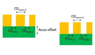
.png)

The 7 nm foundry node is expected to utilize any of or a combination of the following patterning technologies: pitch splitting, self-aligned patterning, and EUV lithography. Each of these technologies carries significant challenges in critical dimension (CD) control as well as pattern placement, all involving neighboring features.
Pitch splitting
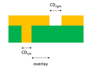
Pitch splitting involves splitting features which are too close together onto different masks, which are exposed successively, followed by litho-etch processing. Due to the use of different exposures, there is always the risk of overlay error between the two exposures, as well as different CDs resulting from the different exposures.
Spacer patterning
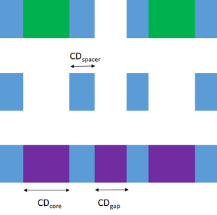
Spacer patterning involves depositing a layer onto pre-patterned features, then etching back to form spacers on the sidewalls of those features, referred to as core features. After removing the core features, the spacers are used as an etch mask to define trenches in the underlying layer. While the spacer CD control is generally excellent, the trench CD may fall into one of two populations, due to the two possibilities of being located where a core feature was located or in the remaining gap. This is known as 'pitch walking'.[19] Generally pitch = core CD + gap CD + 2 * spacer CD, but this does not guarantee core CD = gap CD. For FEOL features like gate or active area isolation (e.g., fins), the trench CD is not as critical as the spacer-defined CD, in which case, spacer patterning is actually the preferred patterning approach.
When self-aligned quadruple patterning (SAQP) is used, there is a second spacer that is utilized, replacing the first one. In this case, the core CD is replaced by core CD - 2* 2nd spacer CD, and the gap CD is replaced by gap CD - 2 * 2nd spacer CD. Thus, some feature dimensions are strictly defined by the second spacer CD, while the remaining feature dimensions are defined by the core CD, core pitch, and first and second spacer CD's. The core CD and core pitch are defined by conventional lithography, while the spacer CDs are independent of lithography. This is actually expected to have less variation than pitch splitting, where an additional exposure defines its own CD, both directly and through overlay.
Spacer-defined lines also require cutting. The cut spots may shift at exposure, resulting in distorted line ends or intrusions into adjacent lines.
EUV lithography
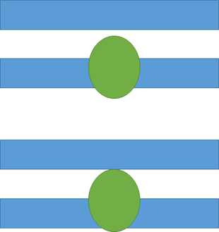
EUV lithography is capable of resolving features below 20 nm in conventional lithography style. However, the 3D reflective nature of the EUV mask results in new anomalies in the imaging. One particular nuisance is the two-bar effect, where a pair of identical bar-shaped features do not focus identically. One feature is essentially in the 'shadow' of the other. Consequently, the two features generally have different CDs which change through focus, and these features also shift position through focus.[20][21] This effect may be similar to what may be encountered with pitch splitting. A related issue is the difference of best focus among features of different pitches.[22]
EUV also has issues with reliably printing all features in a large population; some contacts may be completely missing or lines bridged. These are known as stochastic printing failures.[23] The defect level is on the order of 1K/mm2.[24]
The tip-to-tip gap is hard to control for EUV, largely due to the illumination constraint.[25] A separate exposure(s) for cutting lines is preferred.
Attenuated phase shift masks have been used in production for 90 nm node for adequate focus windows for arbitrarily pitched contacts with the ArF laser wavelength (193 nm),[26][27] whereas this resolution enhancement is not available for EUV.[28][29]
Comparison with previous nodes
Due to these challenges, 7 nm poses unprecedented patterning difficulty in the BEOL. The previous high-volume, long-lived foundry node (Samsung 10 nm, TSMC 16 nm) used pitch splitting for the tighter pitch metal layers.[30][31][32]
7 nm process nodes
The naming of process nodes by different major manufacturers (TSMC, Intel, Samsung, GlobalFoundries) is partially marketing driven and not directly related to any measurable distance on a chip – for example TSMC's 7 nm node is similar in some key dimensions to Intel's 10 nm node. Nevertheless, as of 2017, the technological race to the greatest density was still competitive between the main players, with TSMC, Samsung, and Intel all holding leading positions between the years 2016 and 2017 when measured by the smallest feature size on chip.[33][34]
| ITRS Logic Device
Ground Rules |
Samsung
(proposed) |
TSMC | ||
|---|---|---|---|---|
| Process name[35][36] | 8/7 nm | 11/10 nm | 7 nm | 7 nm |
| Contacted poly pitch / transistor gate pitch (nm) |
42 | 48 | 54 | 54 |
| Interconnect pitch / minimum metal pitch (nm) |
24 | 36 | 36 | 40 |
7 nm process offerings
| Process | Samsung 7LPP[37] | TSMC 7FF[38] | TSMC 7FF+[39] |
|---|---|---|---|
| Minimum (metal) pitch | 36 nm | 40 nm | < 40 nm |
| EUV implementation | Bidirectional metal Contacts |
None | 4 layers |
| EUV-limited wafer output | 1100 wafers/day[40] | N/A | ~ 1000 wafers/day[41] |
| Multipatterning (≥ 2 masks on a layer) |
Fins Gate Contacts Lowest 10 metal layers |
Same as 7FF, with reduction on 4 EUV layers | |
| Release status | 2018 internal release | 2018 production | 2018 release |
References
- ↑ "The iPhone XS & XS Max Review: Unveiling the Silicon Secrets (Page 2:The Apple A12 - First Commercial 7nm Silicon)". AnandTech. 5 Oct 2018. Retrieved 6 Oct 2018.
- 1 2 TSMC ramping up 7nm chip production Monica Chen, Hsinchu; Jessie Shen, DIGITIMES Friday 22 June 2018
- ↑ "Apple's A12 Bionic CPU for the new iPhone XS is ahead of the industry moving to 7nm chip manufacturing tech". CNET. 2018-09-12. Retrieved 2018-09-16.
- ↑ "Apple's A12 Bionic is the first 7-nanometer smartphone chip". Engadget. Retrieved 2018-09-20.
- ↑ IBM Research builds functional 7nm processor
- ↑ IBM Discloses Working Version of a Much Higher-Capacity Chip - NYTimes.com
- ↑ Merritt, Rick (8 Feb 2017), "TSMC, Samsung Diverge at 7nm", www.eetimes.com
- ↑ Parish, Kevin (20 Apr 2016). "Watch out Intel and Samsung: TSMC is gearing up for 7 nm processing with trial production". www.digitaltrends.com.
- ↑ "TSMC Tips 7+, 12, 22nm Nodes | EE Times". EETimes. Retrieved 2017-03-17.
- ↑ Shilov, Anton (5 May 2017), "Samsung and TSMC Roadmaps: 8 and 6 nm Added, Looking at 22ULP and 12FFC", www.anandtech.com, p. 2
- ↑ "GLOBALFOUNDRIES to Deliver Industry's Leading-Performance Offering of 7 nm FinFET Technology" (Press release). September 15, 2016. Retrieved April 8, 2017.
- ↑ Intel Supports American Innovation with $7 Billion Investment in Next-Generation Semiconductor Factory in Arizona: Intel’s Fab 42 will Target Advanced 7 nm Technology and Create More Than 10,000 Jobs in Arizona
- ↑ https://www.bloomberg.com/news/articles/2018-05-22/samsung-says-new-7-nanometer-chip-production-starting-this-year Samsung Says New 7-Nanometer Chip Production Starting This Year
- ↑ "Pushing Boundaries for CPUs and GPUs, AMD Shows Next-Generation of Ryzen, Radeon and EPYC Product Leadership at Computex 2018" (Press release). June 5, 2018.
- ↑ https://www.crn.com/news/components-peripherals/amd-cto-we-went-all-in-on-7nm-cpus
- ↑ https://www.engadget.com/2018/08/28/global-foundries-stops-7-nanometer-chip-production/ Major AMD chip supplier will no longer make next-gen chips
- ↑ "Apple Announces 'iPhone Xs' and 'iPhone Xs Max' With Gold Color, Faster Face ID, and More".
- ↑ "Apple Introduces 7nm A12 Bionic CPU for iPhone XS". Tom's Hardware. 2018-09-12. Retrieved 2018-09-12.
- ↑ M. J. Maslow et al., Proc. SPIE 10587, 1058704 (2018).
- ↑ Y. Nakajima et al., EUVL Symposium 2007, Sapporo.
- ↑ L. de Winter et al., Proc. SPIE 9661, 96610A (2015).
- ↑ M. Burkhardt and A. Raghunathan, Proc. SPIE 9422, 94220X (2015).
- ↑ P. De Bisschop and E. Hendrickx, Proc. SPIE 10583, 105831K (2018).
- ↑ S. Larivière et al., Proc. SPIE 10583, 105830U (2018).
- ↑ E. van Setten et al., Proc. SPIE 9661. 96610G (2015).
- ↑ C-H. Chang et al., Proc. SPIE 5377, 902 (2004).
- ↑ T. Devoivre et al., MTDT 2002.
- ↑ S-S. Yu et al., Proc. SPIE 8679, 86791L (2013).
- ↑ A. Erdmann et al., Proc. SPIE 10583, 1058312 (2018).
- ↑ Samsung's 2nd generation 10nm by LELELELE
- ↑ tsmc 10nm starts
- ↑ 16nm FinFET CMOS
- ↑ Merrit, Rick (16 Jan 2017), "15 Views from a Silicon Summit", www.eetimes.com
- ↑ "Intel Details Cannonlake's Advanced 10nm FinFET Node, Claims Full Generation Lead Over Rivals".
- ↑ "International Technology Roadmap for Semiconductors 2.0 2015 Edition Executive Report" (PDF).
- ↑ "7 nm lithography process".
- ↑ VLSI 2018
- ↑ IEDM 2016
- ↑ EETimes 1333827
- ↑ Samsung DAC 2018 Breakfast
- ↑ TSMC Q1 2018 earnings call transcript, p.12
| Preceded by 10 nm |
CMOS manufacturing processes | Succeeded by 5 nm |