x87
x87 is a floating point-related subset of the x86 architecture instruction set. It originated as an extension of the 8086 instruction set in the form of optional floating point coprocessors that worked in tandem with corresponding x86 CPUs. These microchips had names ending in "87". This was also known as the NPX (Numeric Processor eXtension). Like other extensions to the basic instruction set, x87-instructions are not strictly needed to construct working programs, but provide hardware and microcode implementations of common numerical tasks, allowing these tasks to be performed much faster than corresponding machine code routines can. The x87 instruction set includes instructions for basic floating point operations such as addition, subtraction and comparison, but also for more complex numerical operations, such as the computation of the tangent function and its inverse, for example.
Most x86 processors since the Intel 80486 have had these x87 instructions implemented in the main CPU but the term is sometimes still used to refer to that part of the instruction set. Before x87 instructions were standard in PCs, compilers or programmers had to use rather slow library calls to perform floating-point operations, a method that is still common in (low-cost) embedded systems.
Description
The x87 registers form an 8-level deep non-strict stack structure ranging from ST(0) to ST(7) with registers that can be directly accessed by either operand, using an offset relative to the top, as well as pushed and popped. (This scheme may be compared to how a stack frame may be both pushed/popped and indexed.)
There are instructions to push, calculate, and pop values on top of this stack; unary operations (FSQRT, FPTAN etc.) then implicitly address the topmost ST(0) while binary operations (FADD, FMUL, FCOM, etc.) implicitly address ST(0) and ST(1). The non-strict stack-model also allows binary operations to use ST(0) together with a direct memory operand or with an explicitly specified stack-register, ST(x), in a role similar to a traditional accumulator (a combined destination and left operand). This can also be reversed on an instruction-by-instruction basis with ST(0) as the unmodified operand and ST(x) as the destination. Furthermore, the contents in ST(0) can be exchanged with another stack register using an instruction called FXCH ST(x).
These properties make the x87 stack usable as seven freely addressable registers plus a dedicated accumulator (or as seven independent accumulators). This is especially applicable on superscalar x86 processors (such as the Pentium of 1993 and later) where these exchange instructions (codes D9C8..D9CFh) are optimized down to a zero clock penalty by using one of the integer paths for FXCH ST(x) in parallel with the FPU instruction. Despite being natural and convenient for human assembly language programmers, some compiler writers have found it complicated to construct automatic code generators that schedule x87 code effectively. Such a stack-based interface potentially can minimize the need to save scratch variables in function calls compared with a register-based interface[1] (although, historically, design issues in the original implementation limited that potential[2][3]).
The x87 provides single precision, double precision and 80-bit double-extended precision binary floating-point arithmetic as per the IEEE 754-1985 standard. By default, the x87 processors all use 80-bit double-extended precision internally (to allow for sustained precision over many calculations- see IEEE 754 design rationale). A given sequence of arithmetic operations may thus behave slightly differently compared to a strict single-precision or double-precision IEEE 754 FPU.[4] As this may sometimes be problematic for some semi-numerical calculations written to assume double precision for correct operation, to avoid such problems, the x87 can be configured via a special configuration/status register to automatically round to single or double precision after each operation. Since the introduction of SSE2, the x87 instructions are not as essential as they once were, but remain important as a high precision scalar unit for numerical calculations sensitive to round-off error and requiring the 64-bit mantissa precision and extended range available in the 80-bit format.
Performance
Clock cycle counts for examples of typical x87 FPU instructions (only register-register versions shown here).[5]
The A~B notation (minimum to maximum) covers timing variations dependent on transient pipeline status as well as the arithmetic precision chosen (32, 64 or 80 bits); it also includes variations due to numerical cases (such as the number of set bits, zero, etc.). The L→H notation depicts values corresponding to the lowest (L) and the highest (H) maximum clock frequencies that were available.
| x87 implementation | FADD | FMUL | FDIV | FXCH | FCOM | FSQRT | FPTAN | FPATAN | Max Clock (MHz) |
Peak FMUL (millions/sec) |
FMUL§ rel. 5 MHz 8087 |
|---|---|---|---|---|---|---|---|---|---|---|---|
| 8087 | 70…100 | 90…145 | 193…203 | 10…15 | 40…50 | 180…186 | 30…540 | 250…800 | 5 → 10 | 0.034…0.055 → 0.100…0.111 | 1 → 2× as fast |
| 80287 (original) | 6 → 12 | 0.041…0.066 → 0.083…0.133 | 1.2 → 2.4× | ||||||||
| 80387 (and later 287 models) | 23…34 | 29…57 | 88…91 | 18 | 24 | 122…129 | 191…497 | 314…487 | 16 → 33 | 0.280…0.552 → 0.580…1.1 | ~10 → 20× |
| 80486 (or 80487) | 8…20 | 16 | 73 | 4 | 4 | 83…87 | 200…273 | 218…303 | 16 → 50 | 1.0 → 3.1 | ~18 → 56× |
| Cyrix 6x86, Cyrix MII | 4…7 | 4…6 | 24…34 | 2 | 4 | 59…60 | 117…129 | 97…161 | 66 → 300 | 11…16 → 50…75 | ~320 → 1400× |
| AMD K6 (including K6 II/III) | 2 | 2 | 21…41 | 2 | 3 | 21…41 | ? | ? | 166 → 550 | 83 → 275 | ~1500 → 5000× |
| Pentium / Pentium MMX | 1…3 | 1…3 | 39 | 1 (0*) | 1…4 | 70 | 17…173 | 19…134 | 60 → 300 | 20…60 → 100…300 | ~1100 → 5400× |
| Pentium Pro | 1…3 | 2…5 | 16…56 | 1 | 28…68 | ? | ? | 150 → 200 | 30…75 → 40…100 | ~1400 → 1800× | |
| Pentium II / III | 1…3 | 2…5 | 17…38 | 1 | 27…50 | ? | ? | 233 → 1400 | 47…116 → 280…700 | ~2100 → 13000× | |
| Athlon (K7) | 1…4 | 1…4 | 13…24 | 1…2 | 16…35 | ? | ? | 500 → 2330 | 125…500 → 580…2330 | ~9000 → 42000× | |
| Athlon 64 (K8) | 1000 → 3200 | 250…1000 → 800…3200 | ~18000 → 58000× | ||||||||
| Pentium 4 | 1…5 | 2…7 | 20…43 | multiple cycles | 1 | 20…43 | ? | ? | 1300 → 3800 | 186…650 → 543…1900 | ~11000 → 34000× |
* An effective zero clock delay is often possible, via superscalar execution.
§ The 5 MHz 8087 was the original x87 processor. Compared to typical software-implemented floating point routines on an 8086 (without an 8087), the factors would be even larger, perhaps by another factor of 10 (i.e., a correct floating point addition in assembly language may well consume over 1000 cycles).
Manufacturers
Companies that have designed or manufactured[lower-alpha 1] floating point units compatible with the Intel 8087 or later models include AMD (287, 387, 486DX, 5x86, K5, K6, K7, K8), Chips and Technologies (the Super MATH coprocessors), Cyrix (the FasMath, Cx87SLC, Cx87DLC, etc., 6x86, Cyrix MII), Fujitsu (early Pentium Mobile etc.), Harris Semiconductor (manufactured 80387 and 486DX processors), IBM (various 387 and 486 designs), IDT (the WinChip, C3, C7, Nano, etc.), IIT (the 2C87, 3C87, etc.), LC Technology (the Green MATH coprocessors), National Semiconductor (the Geode GX1, Geode GXm, etc.), NexGen (the Nx587), Rise Technology (the mP6), ST Microelectronics (manufactured 486DX, 5x86, etc.), Texas Instruments (manufactured 486DX processors etc.), Transmeta (the TM5600 and TM5800), ULSI (the Math·Co coprocessors), VIA (the C3, C7, and Nano, etc.), and Xtend (the 83S87SX-25 and other coprocessors).
Architectural generations
8087
The 8087 was the first math coprocessor for 16-bit processors designed by Intel. It was built to be paired with the Intel 8088 or 8086 microprocessors. However, the Intel 8231 floating-point processor was an earlier design. It was a licensed version of AMD's Am9511 of 1977.[6] The Am9511 was primarily intended for the Intel 8080, but, using some amount of glue logic, it was possible to use it with almost any microprocessor (-system) that had a spare interrupt input or interrupt vector available. The family included the 32-bit Am9511 and Am9511A (or Intel 8231/8231A) and the later 64-bit Am9512 (or Intel 8232).
80187
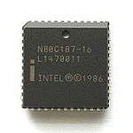
The 80187 (80C187)[7] is the math coprocessor for the Intel 80186 CPU. It is incapable of operating with the 80188, as the 80188 has an 8 bit data bus; the 80188 can only use the 8087. The 80187 did not appear at the same time as the 80186 and 80188, but was in fact launched after the 80287 and the 80387. Although the interface to the main processor is the same as that of the 8087, its core is that of the 80387, and is thus fully IEEE 754 compliant as well as capable of executing all the 80387's extra instructions.[8]
80287
The 80287 (i287) is the math coprocessor for the Intel 80286 series of microprocessors. Intel's models included variants with specified upper frequency limits ranging from 6 up to 12 MHz. Later followed the i80287XL with 387 microarchitecture and the i80287XLT, a special version intended for laptops, as well as other variants.
The 80287XL is actually an 80387SX with a 287 pinout. It contains an internal 3/2 multiplier so that motherboards which ran the coprocessor at 2/3 CPU speed could instead run the FPU at the same speed of the CPU. Other 287 models with 387-like performance are the Intel 80C287, built using CHMOS III, and the AMD 80EC287 manufactured in AMD's CMOS process, using only fully static gates.
The 80287 and 80287XL work with the 80386 microprocessor, and were initially the only coprocessors available for the 80386 until the introduction of the 80387 in 1987. Finally, they were able to work with the Cyrix Cx486SLC. However, for both of these chips the 80387 is strongly preferred for its higher performance and the greater capability of its instruction set.
 6 MHz version of the Intel 80287
 Intel 80287 die shot
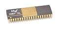 Intel 80287XL
 Intel 80287XLT
80387
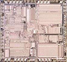
The 80387 (387 or i387) is the first Intel coprocessor to be fully compliant with the IEEE 754-1985 standard. Released in 1987, a full two years after the 386 chip, the i387 includes much improved speed over Intel's previous 8087/80287 coprocessors, and improved characteristics of its trigonometric functions. The 8087 and 80287's FPTAN and FPATAN instructions are limited to an argument in the range ±π/4 (±45°), and the 8087 and 80287 have no direct instructions for the SIN and COS functions.[9]
Without a coprocessor, the 386 normally performs floating-point arithmetic through (slow) software routines, implemented at runtime through a software exception-handler. When a math coprocessor is paired with the 386, the coprocessor performs the floating point arithmetic in hardware, returning results much faster than an (emulating) software library call.
The i387 is compatible only with the standard i386 chip, which has a 32-bit processor bus. The later cost-reduced i386SX, which has a narrower 16-bit data bus, can not interface with the i387's 32-bit bus. The i386SX requires its own coprocessor, the 80387SX, which is compatible with the SX's narrower 16-bit data bus.
 i387
i387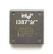 i387SX
 i387DX
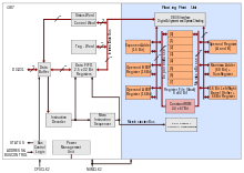 i387 microarchitecture with 16-bit barrel shifter and CORDIC unit
 i386DX with i387DX
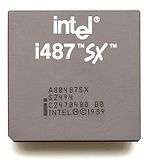
80487
The i487SX (P23N) was marketed as a floating point unit coprocessor for Intel i486SX machines. It actually contained a full-blown i486DX implementation. When installed into an i486SX system, the i487 disabled the main CPU and took over all CPU operations. The i487 took measures to detect the presence of an i486SX and would not function without the original CPU in place.[10]
80587
The Nx587 was the last FPU for x86 to be manufactured separately from the CPU, in this case NexGen's Nx586.
See also
References
- ↑ William Kahan (November 2, 1990). "On the advantages of 8087's stack. Unpublished course notes, Computer Science Division, University of California at Berkeley" (PDF).
- ↑ William Kahan (July 8, 1989). "How Intel 8087 stack overflow/underflow should have been handled" (PDF).
- ↑ Jack Woehr (November 1, 1997). "A conversation with William Kahan".
- ↑ David Monniaux, The pitfalls of verifying floating-point computations, to appear in ACM TOPLAS
- ↑ Numbers are taken from respective processors' data sheets, programming manuals, and optimization manuals.
- ↑ "Arithmetic Processors: Then and Now - The CPU Shack Museum". www.cpushack.com. Retrieved April 14, 2018.
- ↑ "CPU Collection - Model 80187". cpu-info.com. Retrieved April 14, 2018.
- ↑ "HTTP 301 This page has been moved" (PDF). www.datasheetcatalog.org. Retrieved April 14, 2018.
- ↑ Borland Turbo Assembler documentation
- ↑ Intel 487SX at the Free On-line Dictionary of Computing