AMD Radeon Rx 300 series
|
| |
| Release date | 16 June 2015 |
|---|---|
| Codename |
Caribbean Islands[1] Sea Islands Volcanic Islands |
| Architecture |
GCN 1st gen GCN 2nd gen GCN 3rd gen |
| Cards | |
| Entry-level |
Radeon R5 330 Radeon R5 340 Radeon R7 340 Radeon R7 350 |
| Mid-range |
Radeon R7 360 Radeon R7 370 Radeon R9 380 Radeon R9 380X |
| High-end |
Radeon R9 390 Radeon R9 390X |
| Enthusiast |
Radeon R9 Nano Radeon R9 Fury Radeon R9 Fury X Radeon Pro Duo |
| API support | |
| Direct3D | |
| OpenCL | OpenCL 2.0 [2] |
| OpenGL | OpenGL 4.5 (4.6 Windows 7+ and Adrenalin 18.4.1+)[3] [4] [5] [6][7] |
| Vulkan |
Vulkan 1.1 [8] [9] [10] SPIR-V |
| History | |
| Predecessor | Radeon R5/R7/R9 200 series |
| Successor | Radeon 400 series |
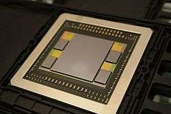
The Radeon R5/R7/R9 300 series is a series of Radeon graphics cards made by Advanced Micro Devices (AMD). All of the GPUs of the series are produced in 28 nm format and use the Graphics Core Next (GCN) micro-architecture.
The GPUs are based on the Fiji architecture. Some of the cards of the series include the flagship AMD Radeon R9 Fury X along with the Radeon R9 Fury and Radeon R9 Nano,[11] which are the first GPUs to feature High Bandwidth Memory (HBM) technology which is faster and more power efficient[12] than current GDDR5 memory. However, the remaining GPUs in the series are based on previous generation GPUs with revised power management and therefore only feature GDDR5 memory. The Radeon 300 series cards including the R9 390X were released on June 18, 2015. The flagship device, the Fury X, was released on June 24, 2015, with the dual-GPU variant, the Radeon Pro Duo, being released on April 26, 2016.[13]
Micro-architecture and instruction set
The R9 380 along with the R9 Fury & Nano series were AMD's first cards to use the third iteration of their GCN instruction set and micro-architecture. The other cards in the series feature first and second gen iterations of GCN. The table below details which GCN-generation each chip belongs to.
Ancillary ASICs
Any ancillary ASICs present on the chips are being developed independently of the core architecture and have their own version name schemes.
Multi-monitor support
The AMD Eyefinity branded on-die display controllers were introduced in September 2009 in the Radeon HD 5000 Series and have been present in all products since.[14]
AMD TrueAudio
AMD TrueAudio was introduced with the AMD Radeon Rx 200 Series, but can only be found on the dies of GCN 1.1 and later products.
Video acceleration
AMD's SIP core for video acceleration, Unified Video Decoder and Video Coding Engine, are found on all GPUs and are supported by AMD Catalyst and by the open-source Radeon graphics driver.
Frame limiter
A completely new feature to the lineup allows users to reduce power consumption by not rendering unnecessary frames. It will be user configurable.
LiquidVR support
LiquidVR is a technology that improves the smoothness of virtual reality. The aim is to reduce latency between hardware so that the hardware can keep up with the user's head movement, eliminating the motion sickness. A particular focus is on dual GPU setups where each GPU will now render for one eye individually of the display.
Virtual super resolution support
Originally introduced with the previous generation R9 285 and R9 290 series graphics cards, this feature allows users to run games with higher image quality by rendering frames at above native resolution. Each frame is then downsampled to native resolution. This process is an alternative to supersampling which is not supported by all games. Virtual super resolution is similar to Dynamic Super Resolution, a feature available on competing nVidia graphics cards, but trades flexibility for increased performance.[15]
OpenCL (API)
OpenCL accelerates many scientific Software Packages against CPU up to factor 10 or 100 and more. Open CL 1.0 to 1.2 are supported for all Chips with Terascale and GCN Architecture. OpenCL 2.0 is supported with GCN 2nd Gen. or 1.2 and higher) [16] For OpenCL 2.1 and 2.2 only Driver Updates are necessary with OpenCL 2.0 conformant Cards.
Vulkan (API)
API Vulkan 1.0 is supported for all with GCN Architecture. Vulkan 1.1 (GCN 2nd Gen. or 1.2 and higher) will be supported with actual drivers in 2018.[17]
Chipset tables
Desktop models
| Model (Codename) |
Launch | Architecture (Fab) |
Transistors Die Size |
Core | Fillrate[lower-alpha 1][lower-alpha 2][lower-alpha 3] | Processing power[lower-alpha 1][lower-alpha 4] (GFLOPS) |
Memory | TBP (W) | Bus interface | Release Price (USD) | ||||||
|---|---|---|---|---|---|---|---|---|---|---|---|---|---|---|---|---|
| Config[lower-alpha 5] | Clock[lower-alpha 1] (MHz) | Pixel (GP/s) | Texture (GT/s) | Single | Double | Bus type & width (bit) |
Size (MiB) | Clock (MT/s) | Band- width (GB/s) | |||||||
| Radeon R5 330 (Oland Pro) |
May 2015 | GCN 1st gen (28 nm) |
1040×106 90 mm2 |
320:20:8 | Unknown 855 |
6.84 |
17.1 |
547.2 |
34.2 |
DDR3 128-bit |
1024 2048 |
1800 | 28.8 | 30 | PCIe 3.0 ×16 | OEM |
| Radeon R5 340 (Oland XT) |
May 2015 | 384:24:8 | Unknown 825 |
6.6 |
19.8 |
633.6 |
39.6 |
DDR3 GDDR5 128-bit |
1024 2048 |
1800 4500 |
72 | 75 | OEM | |||
| Radeon R7 340 (Oland XT) |
May 2015 | 384:24:8 | 730 780 |
5.8 |
17.5 |
560.6 599 |
35 | DDR3 GDDR5 128-bit |
1024 2048 4096 |
1800 4500 |
72 | 75 | OEM | |||
| Radeon R7 350 (Oland XT) |
May 2015 | 384:24:8 | 1000 1050 |
8 | 24 | 768 806.4 |
48 | DDR3 GDDR5 128-bit |
1024 2048 |
1800 4500 |
72 | 75 | OEM | |||
| Radeon R7 350 [18] (Cape Verde XTL) |
February 2016 | 1500×106 123 mm2 |
512:32:16 | 925 | 14.8 | 29.6 | 947.2 | 59.2 | GDDR5 128-bit |
2048 | 4500 | 72 | 75 | PCIe 3.0 ×16 | $89 | |
| Radeon R7 360[19][20] (Bonaire Pro) |
June 2015 | GCN 2nd gen (28 nm) |
2080×106 160 mm2 |
768:48:16 | 1050 | 16.8 | 50.4 | 1612.8 | 100.8 | GDDR5 128-bit |
2048 | 6500 | 104 | 100 | $109 | |
| Radeon R9 360 (Bonaire Pro) |
May 2015 | 768:48:16 | 1000 1050 |
16 | 48 | 1536 1612.8 |
96 | GDDR5 128-bit |
2048 | 6500 | 104 | 85 | OEM | |||
| Radeon R7 370[19] (Pitcairn Pro) |
June 2015 | GCN 1st gen (28 nm) |
2800×106 212 mm2 |
1024:64:32 | 975 | 31.2 | 62.4 | 1996.8 | 124.8 | GDDR5 256-bit |
2048 4096 |
5600 | 179.2 | 110 | $149 $149+ | |
| Radeon R9 370 (Curaçao Pro) |
May 2015 | 1024:64:32 | 950 975 |
30.4 | 60.8 | 1945.6 1996.8 |
121.6 | GDDR5 256-bit |
2048 4096 |
5600 | 179.2 | 150 | OEM | |||
| Radeon R9 370X (Pitcairn XT) |
August 2015 | 1280:80:32 | 1000 | 32 | 80 | 2560 | 160 | GDDR5 256-bit |
2048 4096 |
5600 | 179.2 | 185 | $179 $179+ | |||
| Radeon R9 380 (Tonga Pro) |
May 2015 | GCN 3rd gen (28 nm) |
5000×106 359 mm2 |
1792:112:32 | 918 | 29.4 | 102.8 | 3290 | 206.6 | GDDR5 256-bit |
4096 | 5500 | 176 | 190 | OEM | |
| Radeon R9 380[21] (Tonga Pro) |
June 2015 | 1792:112:32 | 970 | 31.0 | 108.6 | 3476.5 | 217.3 | GDDR5 256-bit |
2048 4096 |
5700 | 182.4[lower-alpha 6] | 190 | $199 $199+ | |||
| Radeon R9 380X[21] (Tonga XT) |
November 2015 | 2048:128:32 | 970 | 31.0 | 124.2 | 3973.1 | 248.3 | GDDR5 256-bit |
4096 | 5700 | 182.4 | 190 | $229 | |||
| Radeon R9 390[21] (Hawaii Pro) |
June 2015 | GCN 2nd gen (28 nm) |
6200×106 438 mm2 |
2560:160:64 | 1000 | 64 | 160 | 5120 | 640 | GDDR5 512-bit |
8192 | 6000 | 384 | 275 | $329 | |
| Radeon R9 390X[21] (Hawaii XT) |
June 2015 | 2816:176:64 | 1050 | 67.2 | 184.8 | 5913.6 | 739.2 | GDDR5 512-bit |
8192 | 6000 | 384 | 275 | $429 | |||
| Radeon R9 Fury[22] (Fiji Pro) |
July 2015 | GCN 3rd gen (28 nm) |
8900×106 596 mm2 |
3584:224:64 | 1000 | 64 | 224 | 7168 | 448 | HBM 4096-bit |
4096 | 1000 | 512 | 275 | $549 | |
| Radeon R9 Nano[23] (Fiji XT) |
August 2015 | 4096:256:64 | 1000 | 64 | 256 | 8192 | 512 | 175 | $649 | |||||||
| Radeon R9 Fury X[21][24] (Fiji XT) |
June 2015 | 4096:256:64 | 1050 | 67.2 | 268.8 | 8601.6 | 537.6 | 275 | $649 | |||||||
| Radeon Pro Duo[25][26][27][28] (Fiji XT) |
April 2016 | 2× 8900×106 2× 596 mm2 |
2× 4096:256:64 | 1000 | 128 | 512 | 16384 | 1024 | HBM 4096-bit |
2× 4096 | 1000 | 2x 512 | 350 | $1499 | ||
| Model (Codename) |
Launch | Architecture (Fab) |
Transistors Die Size |
Config[lower-alpha 5] | Clock[lower-alpha 1] (MHz) | Pixel (GP/s) | Texture (GT/s) | Single | Double | Bus type & width (bit) |
Size (MiB) | Clock (MT/s) | Band- width (GB/s) |
TBP (W) | Bus interface | Release Price (USD) |
| Core | Fillrate[lower-alpha 1][lower-alpha 2][lower-alpha 3] | Processing power[lower-alpha 1][lower-alpha 4] (GFLOPS) |
Memory | |||||||||||||
- 1 2 3 4 5 6 Boost values (if available) are stated below the base value in italic.
- 1 2 Texture fillrate is calculated as the number of Texture Mapping Units multiplied by the base (or boost) core clock speed.
- 1 2 Pixel fillrate is calculated as the number of Render Output Units multiplied by the base (or boost) core clock speed.
- 1 2 Precision performance is calculated from the base (or boost) core clock speed based on a FMA operation. Double precision performance of Hawaii cards is 1/8 of single precision performance, for the other it is 1/16 of single precision performance.
- 1 2 Unified Shaders : Texture Mapping Units : Render Output Units
- ↑ The R9 380 utilizes loss-less color compression which can increase effective memory performance (relative to GCN 1st gen and 2nd gen cards) in certain situations.
Mobile models
| Model (Codename) |
Launch | Architecture (Fab) |
Core | Fillrate[lower-alpha 1][lower-alpha 2][lower-alpha 3] | Processing power[lower-alpha 1][lower-alpha 4] (GFLOPS) |
Memory | TDP (Watts) (GPU only) | |||||
|---|---|---|---|---|---|---|---|---|---|---|---|---|
| Config[lower-alpha 5] | Clock[lower-alpha 1] (MHz) | Texture (GT/s) | Pixel (GP/s) | Bus type & width (bit) |
Size (GiB) | Clock (MT/s) | Band- width (GB/s) | |||||
| Radeon R5 M330[29] (Exo Pro) |
2015 | GCN 1st gen (28 nm) |
320:20:8 | Unknown 1030 |
8.2 | 20.6 | 659.2 | DDR3 64 |
2 4 |
1000 | 14.4 16 |
18 |
| Radeon R5 M335[29] (Exo Pro) |
2015 | 320:20:8 | Unknown 1070 |
8.6 | 21.4 | 684.8 | DDR3 64 |
2 4 |
1100 | 17.6 | Unknown | |
| Radeon R7 M360[30] (Meso XT) |
2015 | 384:24:8 | Unknown 1125 |
9 | 27 | 864 | DDR3 64 |
2 4 |
1000 | 16 | Unknown | |
| Radeon R9 M365X[31] (Strato Pro) |
2015 | 640:40:16 | Unknown 925 |
14.8 | 37 | 1184 | GDDR5 128 |
4 | 1125 | 72 | 50 | |
| Radeon R9 M370X[31] (Strato Pro) |
May 2015 | 640:40:16 | 800 | 12.8 | 32 | 1024 | GDDR5 128 |
2 | 1125 | 72 | 40–45 | |
| Radeon R9 M375[31] (Strato Pro) |
2015 | 640:40:16 | Unknown 1015 |
16.2 | 40.6 | 1299.2 | GDDR5 128 |
4 | 1100 | 35.2 | Unknown | |
| Radeon R9 M375X[31] (Strato Pro) |
2015 | 640:40:16 | Unknown 1015 |
16.2 | 40.6 | 1299.2 | GDDR5 128 |
4 | 1125 | 72 | Unknown | |
| Radeon R9 M380[31] (Strato Pro) |
2015 | 640:40:16 | Unknown 900 |
14.4 | 36 | 1152 | GDDR5 128 |
4 | 1500 | 96 | Unknown | |
| Radeon R9 M385X[31] (Strato) |
2015 | GCN 2nd gen (28 nm) |
896:56:16 | Unknown 1100 |
17.6 | 61.6 | 1971.2 | GDDR5 128 |
4 | 1500 | 96 | ~75 |
| Radeon R9 M390[31] (Pitcairn) |
June 2015 | GCN 1st gen (28 nm) |
1024:64:32 | Unknown 958 |
30.7 | 61.3 | 1962 | GDDR5 256 |
2 | 1365 | 174.7 | ~100 |
| Radeon R9 M390X[31] (Amethyst XT) |
2015 | GCN 3rd gen (28 nm) |
2048:128:32 | Unknown 723 |
23.1 | 92.5 | 2961.4 | GDDR5 256 |
4 | 1250 | 160 | 125 |
| Radeon R9 M395[31] (Amethyst Pro) |
2015 | 1792:112:32 | Unknown 834 |
26.6 | 93.4 | 2989.0 | GDDR5 256 |
2 | 1365 | 174.7 | 125 | |
| Radeon R9 M395X[31] Amethyst XT) |
2015 | 2048:128:32 | Unknown 909 |
29.1 | 116.3 | 3723.3 | GDDR5 256 |
4 | 1365 | 174.7 | 125 | |
- 1 2 3 Boost values (if available) are stated below the base value in italic.
- ↑ Texture fillrate is calculated as the number of Texture Mapping Units multiplied by the base (or boost) core clock speed.
- ↑ Pixel fillrate is calculated as the number of Render Output Units multiplied by the base (or boost) core clock speed.
- ↑ Precision performance is calculated from the base (or boost) core clock speed based on a FMA operation.
- ↑ Unified Shaders : Texture Mapping Units : Render Output Units
Radeon Feature Matrix
The following table shows features of Radeon-branded GPU microarchitectures.
| R100 | R200 | R300 | R400 | R500 | R600 | RV670 | R700 | Evergreen | Northern Islands |
Southern Islands |
Sea Islands |
Volcanic Islands |
Arctic Islands |
Vega | |
|---|---|---|---|---|---|---|---|---|---|---|---|---|---|---|---|
| Released | Apr 2000 | Aug 2001 | Sep 2002 | May 2004 | Oct 2005 | May 2007 | Nov 2007 | Jun 2008 | Sep 2009 | Oct 2010 | Jan 2012 | Sep 2013 | Jun 2015 | Jun 2016 | Jun 2017 |
| AMD support | |||||||||||||||
| Instruction set | Not publicly known | TeraScale instruction set | GCN instruction set | ||||||||||||
| Microarchitecture | TeraScale 1 (VLIW5) | TeraScale 2 (VLIW5) | TeraScale 3 (VLIW4) | GCN 1st gen | GCN 2nd gen | GCN 3rd gen | GCN 4th gen | GCN 5th gen | |||||||
| Type | Fixed pipeline[lower-alpha 1] | Programmable pixel & vertex pipelines | Unified shader model | ||||||||||||
| Direct3D | 7.0 | 8.1 | 9.0 11 (9_2) |
9.0b 11 (9_2) |
9.0c 11 (9_3) |
10.0 11 (10_0) |
10.1 11 (10_1) |
11 (11_0) | 11 (11_1) 12 (11_1) |
11 (12_0) 12 (12_0) |
11 (12_1) 12 (12_1) | ||||
| Shader model | N/A | 1.4 | 2.0+ | 2.0b | 3.0 | 4.0 | 4.1 | 5.0 | 5.1 6.0 | ||||||
| OpenGL | 1.3 | 2.0[lower-alpha 2] | 3.3 | 4.4[lower-alpha 3] | 4.6 with GLSL 4.5 (Linux 4.5+) | ||||||||||
| Vulkan | N/A | Linux Mesa 17+ Win 7+: 1.0 |
1.1 | ||||||||||||
| OpenCL | N/A | Close to Metal | 1.1 | 1.2 | 2.0 (2.1 in Windows Adrenalin, 1.2 in Linux) | ||||||||||
| HSA | N/A | ||||||||||||||
| Power saving | ? | PowerPlay | PowerTune | PowerTune & ZeroCore Power | |||||||||||
| Video decoder ASIC | N/A | Avivo/UVD | UVD+ | UVD 2 | UVD 2.2 | UVD 3 | UVD 4 | UVD 4.2 | UVD 5.0 or 6.0 | UVD 6.3 | UVD 7[32][lower-alpha 4] | ||||
| Video encoding ASIC | N/A | VCE 1.0 | VCE 2.0 | VCE 3.0 or 3.1 | VCE 3.4 | VCE 4.0[32][lower-alpha 4] | |||||||||
| TrueAudio | N/A | Via dedicated DSP | Via shaders | ||||||||||||
| FreeSync | N/A | 1 2 | |||||||||||||
| HDCP[lower-alpha 5] | ? | 1.4 | 1.4 2.2 | ||||||||||||
| PlayReady[lower-alpha 5] | N/A | 3.0 | |||||||||||||
| Max. displays[lower-alpha 6] | 1–2 | 2 | 2–6 | ||||||||||||
| Max. resolution | ? | 2–6 × 2560×1600 | 2–6 × 4096×2160 @ 60 Hz | 2–6 × 5120×2880 @ 60 Hz | 3 × 7680×4320 @ 60 Hz[33] | ||||||||||
/drm/radeon[lower-alpha 7] |
N/A | ||||||||||||||
/drm/amdgpu[lower-alpha 7] |
N/A | Experimental[34] | |||||||||||||
- ↑ The Radeon 100 Series has programmable pixel shaders, but do not fully comply with DirectX 8 or Pixel Shader 1.0. See article on R100's pixel shaders.
- ↑ These series do not fully comply with OpenGL 2+ as the hardware does not support all types of non power of two (NPOT) textures.
- ↑ OpenGL 4+ compliance requires supporting FP64 shaders and these are emulated on some TeraScale chips using 32-bit hardware.
- 1 2 The UVD and VCE were replaced by the Video Core Next (VCN) ASIC in the Raven Ridge APU implementation of Vega.
- 1 2 To play protected video content, it also requires card, operating system, driver, and application support. A compatible HDCP display is also needed for this. HDCP is mandatory for the output of certain audio formats, placing additional constraints on the multimedia setup.
- ↑ More displays may be supported with native DisplayPort connections, or splitting the maximum resolution between multiple monitors with active converters.
- 1 2 DRM (Direct Rendering Manager) is a component of the Linux kernel. Support in this table refers to the most current version.
Graphics device drivers
Proprietary graphics device driver Catalyst
AMD Catalyst is being developed for Microsoft Windows and Linux. As of July 2014, other operating systems are not officially supported. This may be different for the AMD FirePro brand, which is based on identical hardware but features OpenGL-certified graphics device drivers.
AMD Catalyst supports all features advertised for the Radeon brand.
Free and open-source graphics device driver radeon
The free and open-source drivers are primarily developed on and for Linux, but have been ported to other operating systems as well. Each driver is composed out of five parts:
- Linux kernel component DRM
- Linux kernel component KMS driver: basically the device driver for the display controller
- user-space component libDRM
- user-space component in Mesa 3D
- a special and distinct 2D graphics device driver for X.Org Server, which is finally about to be replaced by Glamor
The free and open-source radeon kernel driver supports most of the features implemented into the Radeon line of GPUs.[6]
The radeon kernel driver is not reverse engineered, but based on documentation released by AMD.[35] This drivers still requires proprietary microcode to operate DRM functions and some GPUs may fail to launch the X server if not available.
Free and open-source graphics device driver amdgpu
This new kernel driver is directly supported and developed by AMD. It is available on various Linux distributions, and has been ported to some other operating systems as well. Only GCN GPUs are supported.[6]
Proprietary graphics device driver AMDGPU-PRO
This new driver by AMD is still undergoing development, but can be used on a few supported Linux distributions already (AMD officially supports Ubuntu, RHEL/CentOS).[36] The driver has been experimentally ported to ArchLinux[37] and other distributions. AMDGPU-PRO is set to replace the previous AMD Catalyst driver and is based on the free and open source amdgpu kernel driver. Pre-GCN GPUs are not supported.
See also
References
- ↑ "AMD officially introduces Radeon 300 "Caribbean Islands" series - VideoCardz.com". videocardz.com.
- 1 2 "AMD Catalyst™ Software Suite for AMD Radeon™ 300 Series Graphics Products". AMD. Retrieved 2018-04-20.
- ↑ "AMD Radeon Software Crimson Edition 16.3 Release Notes". AMD. Retrieved 2018-04-20.
- ↑ "AMDGPU-PRO Driver for Linux Release Notes". 2016. Archived from the original on 2016-12-11. Retrieved 2018-04-23.
- ↑ "Mesamatrix". mesamatrix.net. Retrieved 2018-04-22.
- 1 2 3 "RadeonFeature". X.Org Foundation. Retrieved 2018-04-20.
- ↑ https://www.geeks3d.com/20180501/amd-adrenalin-18-4-1-graphics-driver-released-opengl-4-6-vulkan-1-1-70/
- ↑ "Radeon Software Adrenalin Edition 18.3.4 Release Notes". AMD. Retrieved 2018-04-20.
- ↑ "Radeon™ Software for Linux® with Vulkan® 1.1 support". AMD. Retrieved 2018-04-21.
- ↑ "AMD Open Source Driver for Vulkan". GPUOpen. Retrieved 2018-04-20.
- ↑ "AMD R9 390X and AMD Fury". tectomorrow.com.
- ↑ Moammer, Khalid. "HBM 3D Stacked Memory is up to 9X Faster Than GDDR5 – Coming With AMD Pirate Islands R9 300 Series". WCCF Tech. Retrieved 31 January 2015.
- ↑ "AMD's Upcoming Fiji Based Radeon Flagship Is "Fury", R9 390X Is Based On Enhanced Hawaii". WCCFtech.
- ↑ "AMD Eyefinity: FAQ". AMD. 2011-05-17. Retrieved 2014-07-02.
- ↑ Smith, Ryan. "The AMD Radeon R9 Fury X Review". Anandtech. Purch. p. 8. Retrieved 19 August 2015.
- ↑ https://www.khronos.org/conformance/adopters/conformant-products
- ↑ https://www.khronos.org/conformance/adopters/conformant-products
- ↑ http://wccftech.com/amd-radeon-r7-350-graphics-card-launched/
- 1 2 "Radeon™ R7 Series Graphics Cards | AMD". www.amd.com. Retrieved 2017-04-19.
- ↑ btarunr (18 June 2015). "AMD Announces the Radeon R7 300 Series". TechPowerUp. Retrieved 23 January 2016.
- 1 2 3 4 5 "Radeon™ R9 Series Graphics Cards | AMD". www.amd.com. Retrieved 2017-04-19.
- ↑ Mujtaba, Hassan (10 July 2015). "AMD Radeon R9 Fury with Fiji Pro GPU Officially Launched – 4K Ready Performance, Beats the 980 but for $50 More at $549 US". WCCFtech.com. Retrieved 23 January 2016.
- ↑ Mujtaba, Hassan (17 June 2015). "AMD Radeon R9 Fury X, R9 Nano and Fury Unveiled – Fiji GPU Based, HBM Powered, $649 US Priced Small Form Factor Powerhouse". WCCFtech.com. Retrieved 16 June 2015.
- ↑ Moammer, Khalid (17 June 2015). "AMD Unveils $650 R9 Fury X and $550 R9 Fury – Powered By Fiji, World's First HBM GPU". WCCFtech.com. Retrieved 17 June 2015.
- ↑ Garreffa, Anthony (12 March 2016). "AMD's Upcoming Dual-GPU Called Radeon Pro Duo, Not the R9 Fury X2". TweakTown. Retrieved 14 March 2016.
- ↑ Mah Ung, Gordon (14 March 2016). "AMD's $1,500 Dual-GPU Radeon Pro Duo Graphics Card is Built for Virtual Reality". PC World. IDG. Retrieved 14 March 2016.
- ↑ Moammer, Khalid (17 June 2015). "AMD Unveils World's Fastest Graphics Card – Dual Fiji Fury Board". WCCFtech.com. Retrieved 14 March 2016.
- ↑ Williams, Daniel (26 April 2016). "AMD Releases Radeon Pro Duo: Dual Fiji, 350W, $1500". Anandtech. Purch Group. Retrieved 26 April 2016.
- 1 2 "Radeon™ R5 Series Graphics Cards for Notebook PC | AMD". www.amd.com. Retrieved 2017-02-15.
- ↑ "Radeon™ R7 Series Graphics Cards | AMD". www.amd.com. Retrieved 2017-02-15.
- 1 2 3 4 5 6 7 8 9 10 "Radeon™ R9 Series Laptop Graphics Cards | AMD". www.amd.com. Retrieved 2017-02-15.
- 1 2 Killian, Zak (22 March 2017). "AMD publishes patches for Vega support on Linux". Tech Report. Retrieved 23 March 2017.
- ↑ "Radeon's next-generation Vega architecture" (PDF). radeon.com. Radeon Technologies Group (AMD). 13 June 2017.
- ↑ Larabel, Michael (7 December 2016). "The Best Features Of The Linux 4.9 Kernel". Phoronix. Retrieved 7 December 2016.
- ↑ "AMD Developer Guides". Archived from the original on 2013-07-16. Retrieved 2015-01-31.
- ↑ "Radeon Software for Linux Release Notes". support.amd.com. Retrieved 2018-02-01.
- ↑ "AMDGPU - ArchWiki". wiki.archlinux.org. Retrieved 2018-02-01.