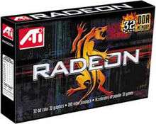
ATi Radeon R100 Series
 | |
| Release date | 2000-2001 |
|---|---|
| Codename | Rage 6C |
| Architecture | Radeon R100 |
| Transistors and fabrication process |
30M 180nm (R100) 30M 180nm (RV100) |
| Cards | |
| Entry-level | 7000 VE, LE |
| Mid-range | 7200 DDR, 7200 SDR |
| High-end |
VIVO, VIVO SE 7500 LE |
| Enthusiast | 7500 |
| API support | |
| Direct3D | Direct3D 7.0 |
| OpenGL | OpenGL 1.3 (T&L) [1][2] |
| History | |
| Predecessor | Rage Series |
| Successor | Radeon 8000 Series |
| CPU supported |
Mobile Athlon XP (320M IGP) Mobile Duron (320M IGP) Pentium 4-M and mobile Pentium 4 (340M IGP, 7000 IGP) |
|---|---|
| Socket supported |
Socket A, Socket 563 (AMD) Socket 478 (Intel) |
| Desktop / mobile chipsets | |
| Performance segment | 7000 IGP |
| Mainstream segment |
320 IGP, 320M IGP 340 IGP, 340M IGP |
| Value segment |
320 IGP, 320M IGP (AMD) 340 IGP, 340M IGP (Intel) |
| Miscellaneous | |
| Release date(s) |
March 13, 2002 (300/300M IGP) March 13, 2003 (7000 IGP) |
| Successor | Radeon 8500/9000/9100 IGP |
The Radeon R100 is the first generation of Radeon graphics chips from ATI Technologies. The line features 3D acceleration based upon Direct3D 7.0 and OpenGL 1.3, and all but the entry-level versions offloading host geometry calculations to a hardware transform and lighting (T&L) engine, a major improvement in features and performance compared to the preceding Rage design. The processors also include 2D GUI acceleration, video acceleration, and multiple display outputs. "R100" refers to the development codename of the initially released GPU of the generation. It is the basis for a variety of other succeeding products.
Development
Architecture
The first-generation Radeon GPU was launched in 2000, and was initially code-named Rage 6 (later R100), as the successor to ATI's aging Rage 128 Pro which was unable to compete with the GeForce 256. The card also had been described as Radeon 256 in the months leading up to its launch, possibly to draw comparisons with the competing Nvidia card, although the moniker was dropped with the launch of the final product.
The R100 was built on a 180 nm semiconductor manufacturing process. Like the GeForce, the Radeon R100 featured a hardware transform and lighting (T&L) engine to perform geometry calculations, freeing up the host computer's CPU. In 3D rendering the processor can write 2 pixels to the framebuffer and sample 3 texture maps per pixel per clock. This is commonly referred to as a 2×3 configuration, or a dual-pipeline design with 3 TMUs per pipe. As for Radeon's competitors, the GeForce 256 is 4×1, GeForce2 GTS is 4×2 and 3dfx Voodoo 5 5500 is a 2×1+2×1 SLI design. Unfortunately, the third texture unit did not get much use in games during the card's lifetime because software was not frequently performing more than dual texturing.
In terms of rendering, its "Pixel Tapestry" architecture allowed for Environment Mapped Bump Mapping (EMBM) and Dot Product (Dot3) Bump Mapping support, offering the most complete Bump Mapping support at the time along with the older Emboss method.[3] Radeon also introduced a new memory bandwidth optimization and overdraw reduction technology called HyperZ. It basically improves the overall efficiency of the 3D rendering processes. Consisting of 3 different functions, it allows the Radeon to perform very competitively compared to competing designs with higher fillrates and bandwidth on paper.
ATI produced a real-time demo for their new card, to showcase its new features. The Radeon's Ark demo presents a science-fiction environment with heavy use of features such as multiple texture layers for image effects and detail. Among the effects are environment-mapped bump mapping, detail textures, glass reflections, mirrors, realistic water simulation, light maps, texture compression, planar reflective surfaces, and portal-based visibility.[4]
In terms of performance, Radeon scores lower than the GeForce2 in most benchmarks, even with HyperZ activated. The performance difference was especially noticeable in 16-bit color, where both the GeForce2 GTS and Voodoo 5 5500 were far ahead. However, the Radeon could close the gap and occasionally outperform its fastest competitor, the GeForce2 GTS, in 32-bit color.
Aside from the new 3D hardware, Radeon also introduced per-pixel video-deinterlacing to ATI's HDTV-capable MPEG-2 engine.
R100's pixel shaders
R100-based GPUs have forward-looking programmable shading capability in their pipelines; however, the chips are not flexible enough to support the Microsoft Direct3D specification for Pixel Shader 1.1. A forum post by an ATI engineer in 2001 clarified this:
...prior to the final release of DirectX 8.0, Microsoft decided that it was better to expose the RADEON's and GeForce{2}'s extended multitexture capabilities via the extensions to SetTextureStageState() instead of via the pixel shader interface. There are various practical technical reasons for this. Much of the same math that can be done with pixel shaders can be done via SetTextureStageState(), especially with the enhancements to SetTextureStageState() in DirectX 8.0. At the end of the day, this means that DirectX 8.0 exposes 99% of what the RADEON can do in its pixel pipe without adding the complexity of a "0.5" pixel shader interface.
Additionally, you have to understand that the phrase "shader" is an incredibly ambiguous graphics term. Basically, we hardware manufacturers started using the word "shader" a lot once we were able to do per-pixel dot products (i.e. the RADEON / GF generation of chips). Even earlier than that, "ATI_shader_op" was our multitexture OpenGL extension on Rage 128 (which was replaced by the multivendor EXT_texture_env_combine extension). Quake III has ".shader" files it uses to describe how materials are lit. These are just a few examples of the use of the word shader in the game industry (nevermind the movie production industry which uses many different types of shaders, including those used by Pixar's RenderMan).
With the final release of DirectX 8.0, the term "shader" has become more crystallized in that it is actually used in the interface that developers use to write their programs rather than just general "industry lingo." In DirectX 8.0, there are two versions of pixel shaders: 1.0 and 1.1. (Future releases of DirectX will have 2.0 shaders, 3.0 shaders and so on.) Because of what I stated earlier, RADEON doesn't support either of the pixel shader versions in DirectX 8.0. Some of you have tweaked the registry and gotten the driver to export a 1.0 pixel shader version number to 3DMark2001. This causes 3DMark2001 to think it can run certain tests. Surely, we shouldn't crash when you do this, but you are forcing the (leaked and/or unsupported) driver down a path it isn't intended to ever go. The chip doesn't support 1.0 or 1.1 pixel shaders, therefore you won't see correct rendering even if we don't crash. The fact that that registry key exists indicates that we did some experiments in the driver, not that we are half way done implementing pixel shaders on RADEON. DirectX 8.0's 1.0 and 1.1 pixel shaders are not supported by RADEON and never will be. The silicon just can't do what is required to support 1.0 or 1.1 shaders. This is also true of GeForce and GeForce2.
Implementations
R100
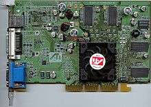
The first versions of the Radeon (R100) were the Radeon DDR, available in Spring 2000 with 32 MB or 64 MB configurations; the 64 MB card had a slightly faster clock speed and added VIVO (video-in video-out) capability. The core speed was 183Mhz and the 5.5 Ns DDR SDRAM memory clock speed was 183 MHz DDR (366 MHz effective). The R100 introduced HyperZ, an early culling technology (maybe inspired by the Tile Rendering present in St Microelectronics PowerVR chips) that became the way to go in graphic evolution and generation by generation rendering optimization, and can be considerend the first non tile rendering-based (and so DX7 compatible) card to use a Z-Buffer optimization. These cards were produced until mid-2001, when they were essentially replaced by the Radeon 7500 (RV200).
A slower and short-lived Radeon SDR (with 32 MB SDRAM memory) was added in mid-2000 to compete with the GeForce2 MX.
Also in 2000, an OEM-only Radeon LE 32MB DDR arrived. Compared to the regular Radeon DDR from ATI, the LE is produced by Athlon Micro from Radeon GPUs that did not meet spec and originally intended for the Asian OEM market. The card runs at a lower 143 MHz clock rate for both RAM and GPU, and its Hyper Z functionality has been disabled. Despite these handicaps, the Radeon LE was competitive with other contemporaries such as the GeForce 2 MX and Radeon SDR. Unlike its rivals, however, the LE has considerable performance potential, as is possible to enable HyperZ through a system registry alteration, plus there is considerable overclocking room. Later drivers do not differentiate the Radeon LE from other Radeon R100 cards and the HyperZ hardware is enabled by default, though there may be visual anomalies on cards with HyperZ hardware that is defective.[5]
In 2001, a short-lived Radeon R100 with 64 MB SDR was released as the Radeon 7200. After this and all older R100 Radeon cards were discontinued, the R100 series was subsequently known as the Radeon 7200, in keeping with ATI's new naming scheme.
RV100
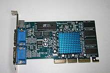
A budget variant of the R100 hardware was created and called the Radeon VE, later known as the Radeon 7000 in 2001 when ATI re-branded its products.
RV100 has only one pixel-pipeline, no hardware T&L, a 64-bit memory bus, and no HyperZ. It did however add HydraVision dual-monitor support and integrated a 2nd RAMDAC into the core (for Hydravision).
From the 3D performance standpoint, the Radeon VE did not fare well against the GeForce2 MX of the same era, though its multi-display support was clearly superior to the GeForce2 MX, however. The Matrox G450 has the best dual-display support out of the GPUs but the slowest 3D performance.
RV100 was the basis for the Mobility Radeon notebook solution.
RV200
The Radeon 7500 (RV200) is basically a die-shrink of the R100 in a new 150 nm manufacturing process. The increased density and various tweaks to the architecture allowed the GPU to function at higher clock speeds. It also allowed the card to operate with asynchronous clock operation, whereas the original R100 was always clocked synchronously with the RAM. It was ATI's first Direct3D 7-compliant GPU to include dual-monitor support (Hydravision).[6]
The Radeon 7500 launched in the second half of 2001 alongside the Radeon 8500 (R200). It used an Accelerated Graphics Port (AGP) 4x interface. Around the time that the Radeon 8500 and 7500 were announced, rival Nvidia released its GeForce 3 Ti500 and Ti200, the 8500 and Ti500 are direct competitors but the 7500 and Ti200 are not.
The desktop Radeon 7500 board frequently came clocked at 290 MHz core and 230 MHz RAM. It competed with the GeForce2 Ti and later on, the GeForce4 MX440.
Radeon Feature Matrix
The following table shows features of Radeon-branded GPU microarchitectures.
| R100 | R200 | R300 | R400 | R500 | R600 | RV670 | R700 | Evergreen | Northern Islands |
Southern Islands |
Sea Islands |
Volcanic Islands |
Arctic Islands |
Vega | |
|---|---|---|---|---|---|---|---|---|---|---|---|---|---|---|---|
| Released | Apr 2000 | Aug 2001 | Sep 2002 | May 2004 | Oct 2005 | May 2007 | Nov 2007 | Jun 2008 | Sep 2009 | Oct 2010 | Jan 2012 | Sep 2013 | Jun 2015 | Jun 2016 | Jun 2017 |
| AMD support | |||||||||||||||
| Instruction set | Not publicly known | TeraScale instruction set | GCN instruction set | ||||||||||||
| Microarchitecture | TeraScale 1 (VLIW5) | TeraScale 2 (VLIW5) | TeraScale 3 (VLIW4) | GCN 1st gen | GCN 2nd gen | GCN 3rd gen | GCN 4th gen | GCN 5th gen | |||||||
| Type | Fixed pipeline[lower-alpha 1] | Programmable pixel & vertex pipelines | Unified shader model | ||||||||||||
| Direct3D | 7.0 | 8.1 | 9.0 11 (9_2) |
9.0b 11 (9_2) |
9.0c 11 (9_3) |
10.0 11 (10_0) |
10.1 11 (10_1) |
11 (11_0) | 11 (11_1) 12 (11_1) |
11 (12_0) 12 (12_0) |
11 (12_1) 12 (12_1) | ||||
| Shader model | N/A | 1.4 | 2.0+ | 2.0b | 3.0 | 4.0 | 4.1 | 5.0 | 5.1 6.0 | ||||||
| OpenGL | 1.3 | 2.0[lower-alpha 2] | 3.3 | 4.4[lower-alpha 3] | 4.6 with GLSL 4.5 (Linux 4.5+) | ||||||||||
| Vulkan | N/A | Linux Mesa 17+ Win 7+: 1.0 |
1.1 | ||||||||||||
| OpenCL | N/A | Close to Metal | 1.1 | 1.2 | 2.0 (2.1 in Windows Adrenalin, 1.2 in Linux) | ||||||||||
| HSA | N/A | ||||||||||||||
| Power saving | ? | PowerPlay | PowerTune | PowerTune & ZeroCore Power | |||||||||||
| Video decoder ASIC | N/A | Avivo/UVD | UVD+ | UVD 2 | UVD 2.2 | UVD 3 | UVD 4 | UVD 4.2 | UVD 5.0 or 6.0 | UVD 6.3 | UVD 7[7][lower-alpha 4] | ||||
| Video encoding ASIC | N/A | VCE 1.0 | VCE 2.0 | VCE 3.0 or 3.1 | VCE 3.4 | VCE 4.0[7][lower-alpha 4] | |||||||||
| TrueAudio | N/A | Via dedicated DSP | Via shaders | ||||||||||||
| FreeSync | N/A | 1 2 | |||||||||||||
| HDCP[lower-alpha 5] | ? | 1.4 | 1.4 2.2 | ||||||||||||
| PlayReady[lower-alpha 5] | N/A | 3.0 | |||||||||||||
| Max. displays[lower-alpha 6] | 1–2 | 2 | 2–6 | ||||||||||||
| Max. resolution | ? | 2–6 × 2560×1600 | 2–6 × 4096×2160 @ 60 Hz | 2–6 × 5120×2880 @ 60 Hz | 3 × 7680×4320 @ 60 Hz[8] | ||||||||||
/drm/radeon[lower-alpha 7] |
N/A | ||||||||||||||
/drm/amdgpu[lower-alpha 7] |
N/A | Experimental[9] | |||||||||||||
- ↑ The Radeon 100 Series has programmable pixel shaders, but do not fully comply with DirectX 8 or Pixel Shader 1.0. See article on R100's pixel shaders.
- ↑ These series do not fully comply with OpenGL 2+ as the hardware does not support all types of non power of two (NPOT) textures.
- ↑ OpenGL 4+ compliance requires supporting FP64 shaders and these are emulated on some TeraScale chips using 32-bit hardware.
- 1 2 The UVD and VCE were replaced by the Video Core Next (VCN) ASIC in the Raven Ridge APU implementation of Vega.
- 1 2 To play protected video content, it also requires card, operating system, driver, and application support. A compatible HDCP display is also needed for this. HDCP is mandatory for the output of certain audio formats, placing additional constraints on the multimedia setup.
- ↑ More displays may be supported with native DisplayPort connections, or splitting the maximum resolution between multiple monitors with active converters.
- 1 2 DRM (Direct Rendering Manager) is a component of the Linux kernel. Support in this table refers to the most current version.
Models
Competing chipsets
- NVIDIA GeForce 256 and GeForce2
- PowerVR Series 3
- 3dfx Voodoo 5
- S3 Savage 2000
See also
References
- ↑ "Mesamatrix". mesamatrix.net. Retrieved 2018-04-22.
- ↑ "RadeonFeature". X.Org Foundation. Retrieved 2018-04-20.
- ↑ https://www.anandtech.com/show/536/6
- ↑ http://alex.vlachos.com/graphics/
- ↑
- ↑
- 1 2 Killian, Zak (22 March 2017). "AMD publishes patches for Vega support on Linux". Tech Report. Retrieved 23 March 2017.
- ↑ "Radeon's next-generation Vega architecture" (PDF). radeon.com. Radeon Technologies Group (AMD). 13 June 2017.
- ↑ Larabel, Michael (7 December 2016). "The Best Features Of The Linux 4.9 Kernel". Phoronix. Retrieved 7 December 2016.
- "ATI Radeon 256 Preview" by Anand Lal Shimpi, AnandTech.com, April 25, 2000, retrieved January 17, 2006
- "ATI Radeon 32MB SDR" by Anand Lal Shimpi, AnandTech.com, October 13, 2000, retrieved January 17, 2006
- "ATI Radeon 64MB DDR" by Matthew Witheiler, AnandTech.com, July 17, 2000, retrieved January 17, 2006
- "Beyond3D 3D Tables" Beyond3D.com, retrieved January 17, 2006
- Vlachos, Alex. Radeon's Ark demo, 2000.