WDC 65C02
The Western Design Center (WDC) 65C02 microprocessor is an enhanced CMOS version of the popular nMOS-based 8-bit MOS Technology 6502. The 65C02 fixed several problems in the original 6502 and added some new instructions. However, its main feature was greatly lowered power usage, on the order of 10 to 20 times less than the NMOS 6502 running at the same speed.[1] The reduced power consumption made the 65C02 useful in portable computer roles and microcontroller systems in industrial settings. It has been used in some home computers, as well as in embedded applications, including medical-grade implanted devices.
Development began in 1981 and samples were released in early 1983.[lower-alpha 1] WDC licensed the design to Synertek, NCR, GTE, and Rockwell Semiconductor. Rockwell's primary interest was in the embedded market and asked for several new commands to be added to aid in this role. These were later copied back into the baseline version, at which point WDC added two new commands of their own to create the W65C02. Sanyo later licensed the design as well, and Seiko Epson produced a further modified version as the HuC6280.
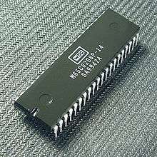
Early versions used 40-pin DIP packaging, and were available in 1, 2 and 4 MHz versions. Later versions were produced in PLCC and QFP packages, as well as PDIP, and with much higher clock speed ratings. The current version from WDC, the W65C02S-14 has a fully static core and officially runs at speeds up to 14 MHz when powered at 5 volts.
Introduction and features
The 65C02 is a low cost, general-purpose 8-bit microprocessor (8-bit registers and data bus) with a 16-bit program counter and address bus. The register set is small, with a single 8-bit accumulator (A), two 8-bit index registers (X and Y), an 8-bit status register (P), and a 16-bit program counter (PC). In addition to the single accumulator, the first 256 bytes of RAM, the "zero page" ($0000 to $00FF), allow faster access through addressing modes that use an 8-bit memory address instead of a 16-bit address. The stack lies in the next 256 bytes, page one ($0100 to $01FF), and cannot be moved or extended. The stack grows downwards with the stack pointer (S) starting at $01FF and decrementing as the stack grows.[2] It has a variable-length instruction set, varying between one and three bytes per instruction.[1]
The basic architecture of the 65C02 is identical to the original 6502, and can be considered a low-power implementation of that design. At 1 MHz, the most popular speed for the original 6502, the 65C02 requires only 20 mW, while the original uses 450 mW, a reduction of over twenty times.[3] The manually optimized core and low power use is intended to make the 65C02 well suited for low power system-on-chip (SoC) designs.[1]
A Verilog hardware description model is available for designing the W65C02S core into an application-specific integrated circuit (ASIC) or a field-programmable gate array (FPGA).[4] As is common in the semiconductor industry, WDC offers a development system, which includes a developer board, an in-circuit emulator (ICE) and a software development system.[5]
The W65C02S–14 is the production version as of 2020, and is available in PDIP, PLCC and QFP packages. The maximum officially supported Ø2 (primary) clock speed is 14 MHz when operated at 5 volts, indicated by the –14 part number suffix (hobbyists have developed 65C02 homebrew systems that run faster than the official rating). The "S" designation indicates that the part has a fully static core, a feature that allows Ø2 to be slowed down or fully stopped in either the high or low state with no loss of data.[6] Typical microprocessors not implemented in CMOS have dynamic cores and will lose their internal register contents (and thus crash) if they are not continuously clocked at a rate between some minimum and maximum specified values.
| 65C02 registers | |||||||||||||||||||||||||||||||||||||||||||||||||||||||||||||||||||||||||||||||||||||||||||||||||||||||||||||||||||||||||||||||||||||||||||||||||||||||||||||||||||||||||||||||||||||||||||
| |||||||||||||||||||||||||||||||||||||||||||||||||||||||||||||||||||||||||||||||||||||||||||||||||||||||||||||||||||||||||||||||||||||||||||||||||||||||||||||||||||||||||||||||||||||||||||
General logic features
- 8-bit data bus
- 16-bit address bus (providing an address space of 64 kB)
- 8-bit arithmetic logic unit (ALU)
- 8-bit processor registers:
- accumulator
- stack pointer
- index registers
- status register
- 16-bit program counter
- 69 instructions, implemented by 212 operation codes
- 16 addressing modes, including zero page addressing

Logic features
- Vector pull (
VPB) output indicates when interrupt vectors are being addressed - Memory lock (
MLB) output indicates to other bus masters when a read-modify-write instruction is being processed - WAit-for-Interrupt (
WAI) and SToP (STP) instructions reduce power consumption, decrease interrupt latency and enable synchronization with external events
Electrical features
- Supply voltage specified at 1.71 V to 5.25 V
- Current consumption (core) of 0.15 and 1.5 mA per MHz at 1.89 V and 5.25 V respectively
- Variable length instruction set, enabling code size optimization over fixed length instruction set processors, results in power savings
- Fully static circuitry allows stopping the clock to conserve power
Clocking features
The W65C02S may be operated at any convenient supply voltage (VDD) between 1.8 and 5 volts (±5%). The data sheet AC characteristics table lists operational characteristics at 5 V at 14 MHz, 3.3 V or 3 V at 8 MHz, 2.5 V at 4 MHz, and 1.8 V at 2 MHz. This information may be an artifact of an earlier data sheet, as a graph indicates that typical devices are capable of operation at higher speeds than suggested by the AC characteristics table, and that reliable operation at 20 MHz should be readily attainable with VDD at 5 volts, assuming the supporting hardware will allow it.
The W65C02S support for arbitrary clock rates allows it to use a clock that runs at a rate ideal for some other part of the system, such as 13.5 MHz (digital SDTV luma sampling rate), 14.31818 MHz (NTSC colour carrier frequency × 4), 14.75 MHz (PAL square pixels), 14.7456 (baud rate crystal), etc., as long as VDD is sufficient to support the frequency. Designer Bill Mensch has pointed out that FMAX is affected by off-chip factors, such as the capacitive load on the microprocessor's pins. Minimizing load by using short signal tracks and fewest devices helps raise FMAX. The PLCC and QFP packages have less pin-to-pin capacitance than the PDIP package, and are more economical in the use of printed circuit board space.
WDC has reported that FPGA realizations of the W65C02S have been successfully operated at 200 MHz.
Comparison with the NMOS 6502
Basic architecture
Although the 65C02 can mostly be thought of as a low-power 6502, it also fixes several bugs found in the original and adds new instructions, addressing modes and features that can assist the programmer in writing smaller and faster-executing programs. It is estimated that the average 6502 assembly language program can be made 10 to 15 percent smaller on the 65C02 and see a similar improvement in performance, largely through avoided memory accesses, as well as use of fewer instructions to accomplish a given task.[1]
Undocumented instructions removed
The original 6502 had 56 instructions, which, when combined with different addressing modes, produced a total of 151 opcodes of the possible 256 8-bit patterns. The remaining 105 unused opcodes were undefined, with the set of codes with low-order 4-bits with 3, 7, B or F left entirely unused, the 2 having only a single opcode.[7]
The 6502 was famous for the way that some of these leftover codes actually performed actions. Due to the way the 6502's instruction decoder worked, simply setting certain bits in the opcode would cause parts of the instruction processing to take place. Some of these opcodes would immediately crash the processor, while other performed useful functions and were even given unofficial assembler mnemonics by users.[8]
The 65C02 added a number of new opcodes that used up a number of these previously "undocumented instruction" slots, for instance, $FF was now used for the new BBS instruction (see below). Those that remained truly unused were set to perform NOPs. Programs that took advantage of these codes will not work on the 65C02, but these codes were always documented as non-operational and should not have been used.[1]
Bug fixes
The original 6502 had several errata when initially launched. Early versions of the processor had a defective ROR (rotate right) instruction, which issue MOS Technology addressed by not documenting the instruction. ROR was fixed very early in the production run and was not an issue for the vast majority of machines using the processor.[9]
In contrast, a notorious bug that is present in all NMOS variants of the 6502 involves the jump instruction (JMP) when using indirect addressing. In this addressing mode, the target address of the JMP instruction is fetched from memory (the jump vector), rather than being an operand to the JMP instruction. For example, JMP ($1234) would fetch the value in memory locations $1234 (least significant byte) and $1235 (most significant byte) and load those values into the program counter, which would then cause the processor to continue execution at the address stored in the jump vector.
The bug appears when the vector address ends in $FF, which is the boundary of a memory page. In this case, JMP will fetch the most significant byte of the target address from $00 of the original page rather than $00 of the new page. Hence JMP ($12FF) would get the least significant byte of the target address at $12FF and the most significant byte of the target address from $1200 rather than $1300. The 65C02 corrected this issue.[1]
More of an oversight than a bug, the state of the (D)ecimal flag in the NMOS 6502's status register is undefined after a reset or interrupt. This means programmers have to set the flag to a known value in order to avoid any bugs related to arithmetic operations. As a result, one finds a CLD instruction (CLear Decimal) in almost all 6502 interrupt handlers, as well as early in the reset code. The 65C02 automatically clears this flag after pushing the status register onto the stack in response any interrupt or in response to a hardware reset, thus placing the processor back into binary arithmetic mode.[10]
During decimal mode arithmetic, the NMOS 6502 will update the (N)egative, o(V)erflow and (Z)ero flags to reflect the result of binary arithmetic, that is, the flags are reflecting a result computed prior to the processor performing decimal correction. In contrast, the 65C02 sets these flags according to the result of decimal arithmetic, at the cost of an extra clock cycle per arithmetic instruction.[10]
When executing a read-modify-write (R-M-W) instruction, such as INC addr, all NMOS variants will do a double write on addr, first rewriting the current value found at addr and then writing the modified value. This behavior can result in difficult-to-resolve bugs if addr is a hardware register. The 65C02 instead performs a double read of addr, followed by a single write.
When performing indexed addressing, if indexing crosses a page bounday all NMOS variants will read from an invalid address before accessing the correct address. As with an R-M-W instruction, this behavior can cause problems when accessing hardware registers via indexing. The 65C02 fixed this problem by performing a dummy read of the instruction opcode when indexing crosses a page boundary. However, this fix introduced a new bug that occurs when the base address is on an even page boundary (which means indexing will never cross into the next page). With the new bug, a dummy read is performed on the base address prior to indexing, such that LDA $1200,X will do a dummy read on $1200 prior to the value of X being added to $1200. Again, if indexing on hardware register addresses, this bug can result in undefined behavior.
If an NMOS 6502 is fetching a BRK (software interrupt) opcode at the same time a hardware interrupt occurs BRK will be ignored as the processor reacts to the interrupt. The 65C02 correctly handles this situation by servicing the interrupt and then executing BRK.
New addressing modes
The 6502 has two indirect addressing modes which dereference through 16-bit addresses stored in page zero:
- Indexed indirect, e.g.
LDA ($10,X), adds the X register to the given page zero address before reading the 16-bit vector. For instance, if X is 5, it reads the 16-bit address from location $15/$16. This is useful when there is an array of pointers in page zero. - Indirect indexed
LDA ($10),Yadds the Y register to the 16-bit vector read from the given page zero address. For instance, if Y is 5, and $10/$11 contains the vector $1000, This reads the value from $1005. This performs pointer-offset addressing.
A downside of this model is that if indexing is not needed, one of the index registers must still be set to zero and used in one of these instructions. The 65C02 added a non-indexed indirect addressing mode LDA ($10) to all instructions that used indexed indirect and indirect indexed modes, freeing up the index registers.[11]
The 6502's JMP instruction had a unique (among 6502 instructions) addressing mode known as "absolute indirect" that read a 16-bit value from a given memory address and then jumped to the address in that 16-bit value. For instance, if memory location $A000 holds $34 and $A001 holds $12, JMP ($A000) would read those two bytes, construct the value $1234, and then jump to that location.
One common use for indirect addressing is to build branch tables, a list of entry points for subroutines that can be accessed using an index. For instance, a device driver might list the entry points for OPEN, CLOSE, READ, etc in a table at $A000. To access the READ function, one would use something similar to JMP ($A004), as it is the 3rd entry in the table (index 2) and each entry is 16-bits. If the driver is updated and the subroutine code moves in memory, any existing code will still work as long as it uses the table to look them up.
The 65C02 added the new "indexed absolute indirect" mode which eased the use of branch tables. This mode added the value of the X register to the absolute address and took the 16-bit address from the resulting location. For instance, to access the READ function from the table above, one would store 4 in X, then JMP ($A000,X). This style of access makes accessing branch tables simpler as a single base address is used in conjunction with an 8-bit offset.[11]
New and modified instructions
In addition to the new addressing modes, the "base model" 65C02 also added a set of new instructions.[12]
INCandDECwith no parameters now increment or decrement the accumulator. This was an odd oversight in the original instruction set, which only includedINX/DEX,INY/DEYandINC addr/DEC addr. Some assemblers use the alternate formsINA/DEAorINC A/DEC A.[12]STZ addr, STore Zero in addr. Replaces the need toLDA #0;STA addrand doesn't change the value in the accumulator. As this task is common in most programs, using STZ can reduce code size, both by eliminating the LDA as well as any code needed to save the value of the accumulator, typically aPHAPLApair.[13]PHX,PLX,PHY,PLY, push and pull the X and Y registers to/from the stack. Previously, only the accumulator and status register had push and pull instructions. X and Y could only be stacked by moving them to the accumulator first withTXAorTYA, thereby corrupting the accumulator contents, then usingPHA.[14]BRA, branch always. Operates like aJMPbut uses a 1-byte relative address like other branches, saving a byte. The speed is often the same as the 3 cycle absoluteJMPunless a page is crossed which would make theBRAversion 1 cycle longer (4 cycles).[15] As the address is relative, it is also useful when writing relocatable code,[13] a common task in the era before memory management units.
Bit manipulation instructions
Both WDC and Rockwell contributed improvements to the bit testing and manipulation functions in the 65C02. WDC added new addressing modes to the BIT instruction that was present in the 6502, as well two new instructions for convenient manipulation of bit fields, a common activity in device drivers.
BIT in the 65C02 adds immediate mode, zero page indexed by X and absolute indexed by X addressing.[12] Immediate mode addressing is particularly convenient in that it is completely non-destructive. For example:
- LDA <register>
- BIT #%00010000
may be used in place of:
- LDA <register>
- AND #%00010000
The former preserves the value loaded from <register> so more than one test can be performed on it. The latter sequence is destructive to the register value.
In addition to the enhancements of the BIT instruction, WDC added two instructions designed to conveniently manipulate bit fields:
TSB addrandTRB addr, Test and Set Bits and Test and Reset Bits.
- A mask in the accumulator (
.A) is logically ANDed with memory at addr, which location may be zero page or absolute. The Z flag in the status register is conditioned according to the result of the logical AND—no other status register flags are affected. Furthermore, bits in addr are set (TSB) or cleared (TRB) according to the mask in.A. Succinctly, TSB performs a logical OR after the logical AND and stores the result of the logical OR at addr, whereas TRB stores the results of the logical AND at addr. In both cases, the Z flag in the status register indicates the result of.A AND addrbefore the content of addr is changed. TRB and TSB thus replace a sequence of instructions, essentially combining the BIT instruction with additional steps to save the computational changes, but in a way that reports the status of the affected value before it is changed.[1]
Rockwell's changes added more bit manipulation instructions for directly setting and testing any bit, and combining the test, clear and branch into a single opcode. The new instructions were available from the start in Rockwell's R65C00 family,[16] but was not part of the original 65C02 specification and not found in versions made by WDC or its other licensees. These were later copied back into the baseline design, and were available in later WDC versions.
Rockwell-specific instructions are:
SMBbit# zp/RMBbit# zp. Set or Reset (clear) bit number bit# in zero page byte zp.
- RMB and SMB are used to clear (RMB) or set (SMB) individual bits in a bit field, each replacing a sequence of three instructions. As RMB and SMB are zero page addressing only, these instructions are limited in usefulness and are primarily of value in systems in which device registers are present in zero page. The bit# component of the instruction is often written as part of the mnemonic, such as
SMB1 $12which sets bit 1 in zero-page address $12. Some assemblers treat bit# as part of the instruction's operand, e.g.,SMB 1,$12, which has the advantage of allowing it to be replaced by a variable name or calculated number.[13]
BBR bit#,offset,addrandBBS bit#,offset,addr, Branch on Bit Set/Reset.
- Same zero-page addressing and limitations as RMB and SMB, but branches to addr if the selected bit is clear (BBR) or set (BBS). As is the case with RMB and SMB, BBR and BBS replace a sequence of three instructions.[13]
Low-power modes
In addition to the new commands above, WDC also added the STP and WAI instructions for supporting low-power modes.
STP, STop the Processor, halted all processing until a hardware reset was issued. This could be used to put a system to "sleep" and then rapidly wake it with a reset. However, this required some external system to maintain memory, and it was not widely used.
WAIt had a similar effect, entering low-power mode, but this instruction woke the processor up again on the reception of an interrupt. Previously, handling an interrupt generally involved running a loop to check if an interrupt has been received, sometimes known as "spinning", checking the type when one is received, and then jumping to the processing code. This meant the processor was running during the entire process.
In contrast, in the 65C02, interrupt code could be written by having a WAI followed immediately by a JSR or JMP to the handler. When the WAI was encountered, processing stopped and the processor went into low-power mode. When the interrupt was received, it immediately processed the JSR and handled the request.
This had the added advantage of slightly improving performance. In the spinning case, the interrupt might arrive in the middle of one of the loop's instructions, and to allow it to restart after returning from the handler, the processor spends one cycle to save its location. With WAI, the processor enters the low-power state in a known location where all instructions are guaranteed to be complete, so when the interrupt arrives it cannot possibly interrupt an instruction, and the processor can safely continue without spending a cycle saving state.
65SC02
The 65SC02 is a variant of the WDC 65C02 without bit instructions.[17]
Notable uses of the 65C02
Home computers
- Apple IIc portable by Apple Computer (NCR 1.023 MHz)
- Enhanced Apple IIe by Apple Computer (1.023 MHz)
- BBC Master home/educational computer, by Acorn Computers Ltd (2 MHz 65SC12 plus optional 4 MHz 65C102 second processor)
- Replica 1 by Briel Computers, a replica of the Apple I hobbyist computer (1 MHz)
- Laser 128 series clones of Apple II
- KIM-1 Modern Replica of the MOS/CBM KIM-1 by Briel Computing
Video game consoles
- Atari Lynx handheld (65SC02 @ ~4 MHz)
- NEC PC Engine aka TurboGrafx-16 (HuC6280 @ 7.16 MHz)[18]
- GameKing handhelds (6 MHz) by Timetop
- Watara Supervision handhelds (65SC02 @ 4 MHz)
Other products
- TurboMaster accelerator cartridge for the Commodore 64 home computer (65C02 @ 4.09 MHz)
- many dedicated chess computers i.e.: Mephisto MMV, Novag Super Constellation, Fidelity Elite and many more (4–20 MHz)
See also
- Interrupts in 65xx processors
- CSG 65CE02, a further enhanced version of the 65C02
Notes
- Wagner's June 1983 article mentions it being available for “several months”. Given typical publication delays at that point this may date it to late 1982.
References
Citations
- Wagner 1983, p. 204.
- Koehn, Philipp (2 March 2018). "6502 Stack" (PDF).
- Taylor & Watford 1984, p. 174.
- "6502 CPU Projects in HDL (for FPGA)".
- "W65C02DB Developer Board".
- "W65C02S-14".
- Parker, Neil. "The 6502/65C02/65C816 Instruction Set Decoded". Neil Parker's Apple II page.
- Vardy, Adam (22 August 1995). "Extra Instructions Of The 65XX Series CPU".
- Steil, Michael (2010-09-28). "Measuring the ROR Bug in the Early MOS 6502".
- "Differences between NMOS 6502 and CMOS 65c02". Retrieved 27 February 2018.
N, V, and Z flags were incorrect after decimal operation (but C was ok).
- Clark, Bruce. "65C02 Opcodes".
- Wagner 1983, p. 200.
- Wagner 1983, p. 203.
- Wagner 1983, pp. 200-201.
- "W65C02S Datasheet" (PDF).
- Wagner 1983, p. 199.
- Zaks, Rodnay. Programming the 6502. p. 348.
- http://archaicpixels.com/HuC6280
Bibliography
- Wagner, Robert (June 1983). "Assembly Lines". Softtalk. pp. 199–204.CS1 maint: ref=harv (link)
- Taylor, Simon; Watford, Bob (July 1984). "6502 revival". Personal Computer World. pp. 174–175.CS1 maint: ref=harv (link)
Further reading
- 65C02 Datasheet; Western Design Center; 32 pages; 2018.
- Programming the 65816 - including the 6502, 65C02, 65802; 1st Ed; David Eyes and Ron Lichty; Prentice Hall; 636 pages; 1986; ISBN 978-0893037895. (archive)
External links
- 65C02 webpage - Western Design Center
- 65xx/65Cxx/65SCxx Differences - CPU World
- 6502/65C02/65C816 Instruction Set Decoded – From Neil Parker's Apple II page