WDC 65C816
The W65C816S (also 65C816 or 65816) is an 8/16-bit microprocessor (MPU) developed and sold by the Western Design Center (WDC). Introduced in 1983,[1] the W65C816S is an enhanced version of the WDC 65C02 8-bit MPU, itself a CMOS enhancement of the venerable MOS Technology 6502 NMOS MPU. The 65C816 was the CPU for the Apple IIGS and in modified form, the Super Nintendo Entertainment System.
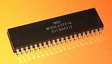
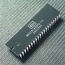 W65C816S in PDIP40 package | |
| General Info | |
|---|---|
| Launched | 1983 |
| Common manufacturer(s) |
|
| Performance | |
| Max. CPU clock rate | 1 MHz to 14 MHz |
| Data width |
|
| Address width | 24 |
| Architecture and classification | |
| Instruction set | 6502 |
| Instructions | 92 |
| Physical specifications | |
| Package(s) |
|
| History | |
| Predecessor |
|
The 65 in the part's designation comes from its 65C02 compatibility mode, and the 816 signifies that the MPU has selectable 8– and 16–bit register sizes. In addition to the availability of 16 bit registers, the W65C816S features extended memory addressing to 24-bits, supporting up to 16 megabytes of random-access memory, an enhanced instruction set, and a 16 bit stack pointer, as well as several new electrical signals for improved system hardware management.
At reset, the W65C816S starts in "emulation mode," meaning it substantially behaves as a 65C02. Thereafter, the W65C816S may be switched to "native mode" with a two instruction sequence, causing it to enable all enhanced features, yet still maintain a substantial degree of backward compatibility with most 65C02 software. However, unlike the PDIP40 version of the 65C02, which is a pin-compatible replacement for its NMOS ancestor, the PDIP40 W65C816S is not pin-compatible with any other 6502 family MPU.
Related to the W65C816S is the W65C802, which had the same internal structure and 16-bit support, but used a 40-pin layout compatible with the original 6502. This allowed it to be used as a drop-in replacement in certain roles. However, the 65C802 could not emit a full 24-bit address, which limited it to 64 kB of memory. The 65C802 and its relatives are no longer produced.
History
In 1981, Bill Mensch, founder and CEO of WDC, began development of the 65C02 with his production partners, primarily Rockwell Semiconductor and Synertek. The primary goal of the 65C02 effort was to move from the original 6502's NMOS process to the 65C02's CMOS, which would allow it to run at much lower power levels, somewhere between 1⁄10 and 1⁄20 when running at the same clock speeds. A number of new opcodes and bug fixes were also worked into the design.[2]
Development of the W65C816S commenced in 1982 after Mensch consulted with Apple Computer on a new version of the Apple II series of personal computers that would, among other things, have improved graphics and sound. Apple wanted an MPU that would be software compatible with the 6502 then in use in the Apple II but with the ability to address more memory, and to load and store 16 bit words. The result was the 65C816, finished in March 1984, with samples provided to both Apple and Atari in the second half of the year and full release in 1985.[3] Mensch was aided during the design process by his sister Kathryn, who was responsible for part of the device's layout.
The same process also led to the 65C802, which was identical inside to the 65C816. Both were produced on the same fabrication lines and diverged only during the last metalization stages when the chip was being connected to the external pins. In the 65C802, those pins had the same layout as the original 6502, which allowed it to be used as a drop-in replacement while still allowing the 16-bit processing of the CPU to be used. However, as it used the original pinout it had only 16 addressing pins, and could therefore only access 64 kB of external memory.[4] Typically, when hardware manufacturers designed a project from the ground up, they used the 65C816 rather than the 65C802, resulting in the latter being withdrawn from production.
Apple subsequently integrated the 65C816 into the Apple IIGS computer. The basic 65C816 design was second-sourced by GTE, Sanyo and others from the mid-to-late 1980s to the early 1990s.
In the 1990s, both the 65C816 and 65C02 were converted to a fully static core, which made it possible to completely stop the processor clock without losing data in any of the registers. This feature, along with the use of asynchronous static RAM, made it possible to produce designs that used minimal power when in a standby state.
As of 2019, the W65C816S is available from WDC in a 40 pin PDIP or PLCC44 package, as well as a core for ASIC integration (for example Winbond's W55V9x series of TV Edutainment ICs). WDC, itself a fabless semiconductor company, works with various foundries to produce the W65C816S, as well as other compatible products. Discrete processors are available through a number of electronics distributors. For designers who wish to include W65C816S functionality into a custom ASIC, WDC offers RTL (register-transfer level) code in Verilog.
Features
WDC 65816 features:
| WDC 65816 registers | |||||||||||||||||||||||||||||||||||||||||||||||||||||||||||||||||||||||||||||||||||||||||||||||||||||||||||||||||||||||||||||||||||||||||||||||||||||||||||||||||||||||||||||||||||||||||||||||||||||||||||||||||||||||||||||||||||||||||||||||||||||||||||||||||||||||||||||||||||||||||||||||||||||||||||||||||||||||||||||||||||||
| |||||||||||||||||||||||||||||||||||||||||||||||||||||||||||||||||||||||||||||||||||||||||||||||||||||||||||||||||||||||||||||||||||||||||||||||||||||||||||||||||||||||||||||||||||||||||||||||||||||||||||||||||||||||||||||||||||||||||||||||||||||||||||||||||||||||||||||||||||||||||||||||||||||||||||||||||||||||||||||||||||||
- Fully static CMOS design for low power consumption (300µA at 1MHz) and increased noise immunity.
- Wide operating voltage range: 1.8V to 5.0V ± 5%.
- Wide operating frequency range, up to 14 MHz, using a single-phase clock source.
- Emulation mode allows software compatibility with the 6502/6510, excepting undocumented opcodes (which in 65C02 act as NOPs).
- 24-bit memory addressing provides access to 16MB of memory space.
- 16-bit ALU, accumulator (A), stack pointer (SP), and index registers (X and Y).
- 16-bit Direct Page register (D).
- 8-bit Data Bank (DB) and Program Bank (PB) registers, generating bits 16-23 of 24-bit data and code addresses.
- Valid Data Address (VDA) and Valid Program Address (VPA) outputs for dual cache and cycle steal DMA implementation.
- Vector Pull (VPB) output to indicate when an interrupt vector is being addressed.
- Abort (ABORTB) input and associated vector supports processor repairs of bus error conditions, such as page faults and memory access violations.
- Separate program and data bank registers allow program segmentation or 16MB linear addressing (data only).
- Direct register and stack relative addressing provides capability for reentrant, recursive and re-locatable programming.
- 24 addressing modes—13 original 6502 modes with 92 instructions using 256 op codes, including most new opcodes implemented in the 65C02.
- Block-copy instructions, allowing rapid copying of data structures from one area of RAM to another with minimal code.
- Wait-for-Interrupt (WAI) and Stop-the-Clock (STP) instructions further reduce power consumption, decrease interrupt latency and allows synchronization with external events.
- Co-Processor (COP) instruction with associated vector supports co-processor configurations, e.g., floating point processors
- Reserved "escape" (WDM) instruction for future two-byte opcodes and a link to future designs. (WDM is the initials of W65C816S designer William D. Mensch.)
Comparison with earlier models
Two modes
The 65C816 has two operating modes, "emulation mode," in which the 16-bit operations are invisible—the index registers are forced to eight bits— and the chip appears to be very similar to the 65C02, with to the same cycle timings for the opcodes, and "native mode," which exposes all new features. The CPU automatically returns to emulation mode when it is powered on or reset, which allows it to replace a 65C02, assuming one makes the required circuit changes to accommodate the different pin layout.[2]
16-bit registers
The most obvious change to the 65C816 when running in 16-bit mode is the expansion of the various registers from 8-bit to 16-bit values. This affects the accumulator (A), the X and Y index registers, and the stack pointer (SP). It does not affect the program counter (PC), which had always been 16-bit.[5]
When running in native mode, two bits in the status register change their meaning. In the original 6502, bits 4 and 5 were not used, although bit 4 was sometimes referred to as the B(reak) flag. In native mode, bit 4 becomes the x flag and bit 5 becomes the m flag. These bits control whether or not the index registers (x) and/or accumulator/memory (m) are 8-bit or 16-bit values. Zeros in these bits indicate 16-bit values, ones indicate 8-bit values. These bits are normally not present when the chip is started up, but are switched on and set to one when switched to native mode.[5]
It might not be immediately obvious why one would want to use the now 16-bit registers in 8-bit mode; however, switching to 8-bit mode using the new SEP (SEt bit in Processor status) and REP (REset) instructions means that all subsequent instructions accessing those registers will only read a single byte instead of two. For instance, if the m bit is set to 1, when an LDA $1234 instruction is issued, only a single byte at address $1234 will be read, thereby reducing the number of cycles needed to execute the instruction.[6] This is particularly useful when dealing with 8-bit character data, for instance.[7]
When running in 16-bit mode, operations on the registers affect all 16 bits. A memory access with a register set to 16 bits will access two contiguous bytes of memory, at the cost of one extra clock cycle. In particular, a read-modify-write instruction, such as ROR <addr>, when used while the accumulator is set to 16 bits, will affect two contiguous bytes of memory, not one. Similarly, all arithmetic and logical operations will be 16-bit operations.[8]
24-bit addressing
The other major change to the system while running in native mode is that the memory model is expanded to a 24-bit format from the original 16-bit format of the 6502. This is handled using two 8-bit offset registers, the Data Bank Register (DB) and the Program Bank Register (PB). Addresses in the code remain in the original 16-bit format, but the values in the DB and PB are prepended to form a 24-bit address in main memory. This means that instructions can access data within a 64KB bank, and if data outside that bank needs to be accessed, DB has to change or "long" addressing must be used (that is, specification of a 24-bit address as an operand to the instruction).
PB determines from which 64KB bank the processor will fetch instructions—there is no programmatic means by which PB can be directly changed. Branches and 16-bit jumps or 16-bit subroutine calls are generally limited to the bank in PB (JMP(<addr>) always fetches the target address from bank $00). A 24-bit "long" jump or subroutine call is possible, which overcomes the normal 64 KB program size limit.[5]
A further addition to the register set is the 16-bit Direct Page Register (DP), which sets the base address for what was formerly called the zero page, but now referred to as direct page. Direct page addressing uses an 8-bit address, which results in faster access than when a 16- or 24-bit address is used. Also, some addressing modes that offer indirection are only possible on direct page. In the 65(C)02, the direct page is always the first 256 bytes of memory, thus "zero page." In native mode, the 65C816 can relocate direct (zero) page anywhere in the first 64KB of memory by writing the starting address into DP. There is a one-cycle access penalty if DP is not set to an even page boundary.[9]
Switching between modes
The current mode of operation is stored in the emulation (E) bit. Having already added the new x and m bits to the previous set of six flags in the status register (SR), there were not enough bits left to hold the new mode bit. Instead, a unique solution was used in which the mode bit was left "invisible", unable to be directly accessed. The new XCE (eXchange Carry with Emulation) instruction exchanges the value of the emulation bit with the C(arry) bit, bit 0 in the status register. For instance, if one wants to enter native mode after the processor has started up, one would use CLC to CLear the Carry bit, and then XCE to write it to the emulation bit.[10] Returning to 65C02 emulation mode uses SEC followed by XCE.[7]
Internally, the 65C816 is a fully 16-bit design. The m and x bits in SR determine how the user registers (accumulator and index) appear to the rest of the system. Upon reset, the 65C816 starts in 65C02 emulation mode, in which m and x are set to 1 and cannot be changed. Hence the registers appear to the rest of the system as 8 bits. The most significant byte (MSB) of the accumulator (the B-accumulator) is not directly accessible but can be swapped with the least significant byte (LSB) of the accumulator (the A-accumulator) by using the XBA instruction. There is no corresponding operation for the index registers (.X and .Y).
Upon being switched to native mode, the MSB of .X and .Y will be zero, and the B-accumulator will be unchanged. If the m bit in SR is cleared, the B-accumulator will "ganged" to the A-accumulator to form a 16-bit register. A load/store or arithmetic/logical operation involving the accumulator and/or memory will be a 16-bit operation—two bus cycles are required to fetch/store a 16-bit value.
If the x bit in SR is cleared, both index registers will be set to 16-bits. If used to index an address, e.g., LDA SOMEWHERE,X, the 16-bit value in the index register will be added to the base address to form the effective address.
If the m bit in SR is set the accumulator will return to being an 8-bit register and subsequent operations on the accumulator, with a few exceptions, will be 8-bit operations. The B-accumulator will retain the value it had when the accumulator was operating in 16-bit mode. The exceptions are the instructions that transfer the direct page register (DP) and stack pointer (SP) to/from the accumulator. These operations are always 16-bits wide in native mode, regardless of the condition of the m bit in the status register.
If the x bit in SR is set, not only will the index registers return to being 8 bits, whatever was in the MSB while in 16-bit mode will be lost, something an assembly language programmer cannot afford to forget.[11]
Applications
Systems based on 65816 variants:
- Acorn Communicator
- Apple IIGS
- Super Nintendo Entertainment System: the console's Ricoh 5A22 CPU is based on the 65C816
- Additionally, 30+ Super NES games include the Nintendo SA1, a 65C816-based co-processor chip, in each cartridge.
It is also used in the C-One and SuperCPU enhancements for the Commodore 64.
See also
References
Citations
- Chronology of Microprocessors (1980-1989)
- Eyes & Lichty 1986, p. 42.
- Eyes & Lichty 1986, p. 44.
- Eyes & Lichty 1986, p. 45.
- Eyes & Lichty 1986, p. 46.
- Eyes & Lichty 1986, p. 50.
- Eyes & Lichty 1986, p. 65.
- Eyes & Lichty 1986, p. 52.
- Eyes & Lichty 1986, p. 48.
- Eyes & Lichty 1986, p. 64.
- Eyes & Lichty 1986, p. 51.
Bibliography
- Eyes, David; Lichty, Ron (1986). Programming the 65816 - including the 6502, 65C02, 65802. Prentice Hall. ISBN 978-0893037895.CS1 maint: ref=harv (link)
Further reading
- 65C816 Datasheet; Western Design Center; 55 pages; 2018.
External links
- 65C816 webpage - Western Design Center
- 6502/65C02/65C816 Instruction Set decoded
- 65816/65C816 Technical Documents - zophar.net
- A 6502 Programmer's Introduction to the 65816 – A Commodore World article by Brett Tabke; includes CMD's instruction set summary
- Investigating 65C816 Interrupts – An extensive discussion of interrupt processing on the 65C816
This article is based on material taken from the Free On-line Dictionary of Computing prior to 1 November 2008 and incorporated under the "relicensing" terms of the GFDL, version 1.3 or later.