Transistor count
The transistor count is the number of transistors on an integrated circuit (IC). It typically refers to the number of MOSFETs (metal-oxide-semiconductor field-effect transistors, or MOS transistors) on an IC chip, as all modern ICs use MOSFETs. It is the most common measure of IC complexity (although the majority of transistors in modern microprocessors are contained in the cache memories, which consist mostly of the same memory cell circuits replicated many times). The rate at which MOS transistor counts have increased generally follows Moore's law, which observed that the transistor count doubles approximately every two years.
As of 2019, the largest transistor count in a commercially available microprocessor is 39.54 billion MOSFETs, in AMD's Zen 2 based Epyc Rome, which is a 3D integrated circuit (with eight dies in a single package) fabricated using TSMC's 7 nm FinFET semiconductor manufacturing process.[1][2] As of 2020, the highest transistor count in a graphics processing unit (GPU) is Nvidia's GA100 Ampere with 54 billion MOSFETs, manufactured using TSMC's 7 nm process.[3] As of 2019, the highest transistor count in any IC chip is Samsung's 1 TB eUFS (3D-stacked) V-NAND flash memory chip, with 2 trillion floating-gate MOSFETs (4 bits per transistor).[4] As of 2019, the highest transistor count in a non-memory chip is a deep learning engine called the Wafer Scale Engine by Cerebras, using a special design to route around any non-functional core on the device; it has 1.2 trillion MOSFETs, manufactured using TSMC's 16 nm FinFET process.[5][6][7][8]
In terms of computer systems that consist of numerous integrated circuits, the supercomputer with the highest transistor count as of 2016 is the Chinese-designed Sunway TaihuLight, which has for all CPUs/nodes (1 trillion for the 10 million cores and for RAM 1015 for the 1.3 million GB) combined "about 400 trillion transistors in the processing part of the hardware" and "the DRAM includes about 12 quadrillion transistors, and that's about 97 percent of all the transistors."[9] To compare, the smallest computer, as of 2018 dwarfed by a grain of rice, has on the order of 100,000 transistors, and the one, fully programmable, with the fewest transistors ever has 130 transistors or fewer.
In terms of the total number of transistors in existence, it has been estimated that a total of 13 sextillion (1.3×10²²) MOSFETs have been manufactured worldwide between 1960 and 2018, accounting for at least 99.9% of all transistors. This makes the MOSFET the most widely manufactured device in history.[10]
Transistor count
Among the earliest products to use transistors were portable transistor radios, introduced in 1954, which typically used 4 to 8 transistors, often advertising the number on the radio's case. However, early junction transistors were relatively bulky devices that were difficult to manufacture on a mass-production basis, limiting the transistor counts and restricting their usage to a number of specialised applications.[11]
The MOSFET (MOS transistor), invented by Mohamed Atalla and Dawon Kahng at Bell Labs in 1959,[12] was the first truly compact transistor that could be miniaturised and mass-produced for a wide range of uses.[11] The MOSFET made it possible to build high-density integrated circuits (ICs),[13] enabling Moore's law[14][15] and very large-scale integration.[16] Atalla first proposed the concept of the MOS integrated circuit (MOS IC) chip in 1960, followed by Kahng in 1961, both noting that the MOSFET's ease of fabrication made it useful for integrated circuits.[11][17] The earliest experimental MOS IC to be demonstrated was a 16-transistor chip built by Fred Heiman and Steven Hofstein at RCA Laboratories in 1962.[15] Further large-scale integration was made possible with an improvement in MOSFET semiconductor device fabrication, the CMOS process, developed by Chih-Tang Sah and Frank Wanlass at Fairchild Semiconductor in 1963.[18]
Microprocessors
A microprocessor incorporates the functions of a computer's central processing unit on a single integrated circuit. It is a multi-purpose, programmable device that accepts digital data as input, processes it according to instructions stored in its memory, and provides results as output.
The development of MOS integrated circuit technology in the 1960s led to the development of the first microprocessors.[19] The 20-bit MP944, developed by Garrett AiResearch for the U.S. Navy's F-14 Tomcat fighter in 1970, is considered by its designer Ray Holt to be the first microprocessor.[20] It was a multi-chip microprocessor, fabricated on six MOS chips. However, it was classified by the Navy until 1998. The 4-bit Intel 4004, released in 1971, was the first single-chip microprocessor. It was made possible with an improvement in MOSFET design, MOS silicon-gate technology (SGT), developed in 1968 at Fairchild Semiconductor by Federico Faggin, who went on to use MOS SGT technology to develop the 4004 with Marcian Hoff, Stanley Mazor and Masatoshi Shima at Intel.[19]
All chips over e.g. a million transistors have lots of memory, usually cache memories in level 1 and 2 or more levels, accounting for most transistors on microprocessors in modern times, where large caches have become the norm. The level 1 caches of the Pentium Pro die accounted for over 14% of its transistors, while the much larger L2 cache was on a separate die, but on-package, so it's not included in the transistor count. Later chips included more levels, L2 or even L3 on-chip. The last DEC Alpha chip made has 90% of it for cache.[21]
While Intel's i960CA small cache of 1 KB, at about 50,000 transistors, isn't a big part of the chip, it alone would have been very large in early microprocessors. In the ARM 3 chip, with 4 KB, the cache was over 63% of the chip, and in the Intel 80486 its larger cache is only over a third of it because the rest of the chip is more complex. So cache memories are the largest factor, except for in early chips with smaller caches or even earlier chips with no cache at all. Then the inherent complexity, e.g. number of instructions, is the dominant factor, more than e.g. the memory the registers of the chip represent.
| Processor | MOS transistor count | Date of introduction |
Designer | MOS process |
Area |
|---|---|---|---|---|---|
| MP944 (20-bit, 6-chip) | ? | 1970[20][lower-alpha 1] | Garrett AiResearch | ? | ? |
| Intel 4004 (4-bit, 16-pin) | 2,250 | 1971 | Intel | 10,000 nm | 12 mm2 |
| TMX 1795 (?-bit, 24-pin) | 3,078[22] | 1971 | Texas Instruments | ? nm | 30 mm2 |
| Intel 8008 (8-bit, 18-pin) | 3,500 | 1972 | Intel | 10,000 nm | 14 mm2 |
| NEC μCOM-4 (4-bit, 42-pin) | 2,500[23][24] | 1973 | NEC | 7,500 nm[25] | ? |
| Toshiba TLCS-12 (12-bit) | 11,000+[26] | 1973 | Toshiba | 6,000 nm | 32 mm2 |
| Intel 4040 (4-bit, 16-pin) | 3,000 | 1974 | Intel | 10,000 nm | 12 mm2 |
| Motorola 6800 (8-bit, 40-pin) | 4,100 | 1974 | Motorola | 6,000 nm | 16 mm2 |
| Intel 8080 (8-bit, 40-pin) | 6,000 | 1974 | Intel | 6,000 nm | 20 mm2 |
| TMS 1000 (4-bit, 28-pin) | 8,000 | 1974[27] | Texas Instruments | 8,000 nm | 11 mm2 |
| MOS Technology 6502 (8-bit, 40-pin) | 4,528[lower-alpha 2][28] | 1975 | MOS Technology | 8,000 nm | 21 mm2 |
| Intersil IM6100 (12-bit, 40-pin; clone of PDP-8) | 4,000 | 1975 | Intersil | ||
| CDP 1801 (8-bit, 2-chip, 40-pin) | 5,000 | 1975 | RCA | ||
| RCA 1802 (8-bit, 40-pin) | 5,000 | 1976 | RCA | 5,000 nm | 27 mm2 |
| Zilog Z80 (8-bit, 4-bit ALU, 40-pin) | 8,500[lower-alpha 3] | 1976 | Zilog | 4,000 nm | 18 mm2 |
| Intel 8085 (8-bit, 40-pin) | 6,500 | 1976 | Intel | 3,000 nm | 20 mm2 |
| TMS9900 (16-bit) | 8,000 | 1976 | Texas Instruments | ||
| Motorola MC14500B (1-bit, 16-pin) | ? | 1977 | Motorola | ? | ? |
| Bellmac-8 (8-bit) | 7,000 | 1977 | Bell Labs | 5,000 nm | |
| Motorola 6809 (8-bit with some 16-bit features, 40-pin) | 9,000 | 1978 | Motorola | 5,000 nm | 21 mm2 |
| Intel 8086 (16-bit, 40-pin) | 29,000 | 1978 | Intel | 3,000 nm | 33 mm2 |
| Zilog Z8000 (16-bit) | 17,500[29] | 1979 | Zilog | ||
| Intel 8088 (16-bit, 8-bit data bus) | 29,000 | 1979 | Intel | 3,000 nm | 33 mm2 |
| Motorola 68000 (16/32-bit, 32-bit registers, 16-bit ALU) | 68,000[30] | 1979 | Motorola | 3,500 nm | 44 mm2 |
| Intel 8051 (8-bit, 40-pin) | 50,000 | 1980 | Intel | ||
| WDC 65C02 | 11,500[31] | 1981 | WDC | 3,000 nm | 6 mm2 |
| ROMP (32-bit) | 45,000 | 1981 | IBM | 2,000 nm | |
| Intel 80186 (16-bit, 68-pin) | 55,000 | 1982 | Intel | 3,000 nm | 60 mm2 |
| Intel 80286 (16-bit, 68-pin) | 134,000 | 1982 | Intel | 1,500 nm | 49 mm2 |
| WDC 65C816 (8/16-bit) | 22,000[32] | 1983 | WDC | 3,000 nm[33] | 9 mm2 |
| NEC V20 | 63,000 | 1984 | NEC | ||
| Motorola 68020 (32-bit; 114 pins used) | 190,000[34] | 1984 | Motorola | 2,000 nm | 85 mm2 |
| Intel 80386 (32-bit, 132-pin; no cache) | 275,000 | 1985 | Intel | 1,500 nm | 104 mm2 |
| ARM 1 (32-bit; no cache) | 25,000[34] | 1985 | Acorn | 3,000 nm | 50 mm2 |
| Novix NC4016 (16-bit) | 16,000[35] | 1985[36] | Harris Corporation | 3,000 nm[37] | |
| SPARC MB86900 (32-bit; no cache) | 110,000[38] | 1986 | Fujitsu | 1,200 nm | |
| NEC V60[39] (32-bit; no cache) | 375,000 | 1986 | NEC | 1,500 nm | |
| ARM 2 (32-bit, 84-pin; no cache) | 27,000[40][34] | 1986 | Acorn | 2,000 nm | 30.25 mm2 |
| Z80000 (32-bit; very small cache) | 91,000 | 1986 | Zilog | ||
| NEC V70[39] (32-bit; no cache) | 385,000 | 1987 | NEC | 1,500 nm | |
| Hitachi Gmicro/200[41] | 730,000 | 1987 | Hitachi | 1,000 nm | |
| Motorola 68030 (32-bit, very small caches) | 273,000 | 1987 | Motorola | 800 nm | 102 mm2 |
| TI Explorer's 32-bit Lisp machine chip | 553,000[42] | 1987 | Texas Instruments | 2,000 nm[43] | |
| DEC WRL MultiTitan | 180,000[44] | 1988 | DEC WRL | 1,500 nm | 61 mm2 |
| Intel i960 (32-bit, 33-bit memory subsystem, no cache) | 250,000[45] | 1988 | Intel | 1,500 nm[46] | |
| Intel i960CA (32-bit, cache) | 600,000[46] | 1989 | Intel | 800 nm | 143 mm2 |
| Intel i860 (32/64-bit, 128-bit SIMD, cache, VLIW) | 1,000,000[47] | 1989 | Intel | ||
| Intel 80486 (32-bit, 4 KB cache) | 1,180,235 | 1989 | Intel | 1000 nm | 173 mm2 |
| ARM 3 (32-bit, 4 KB cache) | 310,000 | 1989 | Acorn | 1,500 nm | 87 mm2 |
| Motorola 68040 (32-bit, 8 KB caches) | 1,200,000 | 1990 | Motorola | 650 nm | 152 mm2 |
| R4000 (64-bit, 16 KB of caches) | 1,350,000 | 1991 | MIPS | 1,000 nm | 213 mm2 |
| ARM 6 (32-bit, no cache for this 60 variant) | 35,000 | 1991 | ARM | 800 nm | |
| Hitachi SH-1 (32-bit, no cache) | 600,000[48] | 1992[49] | Hitachi | 800 nm | 10 mm2 |
| Intel i960CF (32-bit, cache) | 900,000[46] | 1992 | Intel | 125 mm2 | |
| DEC Alpha 21064 (64-bit, 290-pin; 16 KB of caches) | 1,680,000 | 1992 | DEC | 750 nm | 233.52 mm2 |
| Hitachi HARP-1 (32-bit, cache) | 2,800,000[50] | 1993 | Hitachi | 500 nm | 267 mm2 |
| Pentium (32-bit, 16 KB of caches) | 3,100,000 | 1993 | Intel | 800 nm | 294 mm2 |
| ARM700 (32-bit; 8 KB cache) | 578,977[51] | 1994 | ARM | 700 nm | 68.51 mm2 |
| MuP21 (21-bit,[52] 40-pin; includes video) | 7,000[53] | 1994 | Offete Enterprises | 1200 nm | |
| Motorola 68060 (32-bit, 16 KB of caches) | 2,500,000 | 1994 | Motorola | 600 nm | 218 mm2 |
| SA-110 (32-bit, 32 KB of caches) | 2,500,000[34] | 1995 | Acorn/DEC/Apple | 350 nm | 50 mm2 |
| Pentium Pro (32-bit, 16 KB of caches;[54] L2 cache on-package, but on separate die) | 5,500,000[55] | 1995 | Intel | 500 nm | 307 mm2 |
| AMD K5 (32-bit, caches) | 4,300,000 | 1996 | AMD | 500 nm | 251 mm2 |
| Hitachi SH-4 (32-bit, caches) | 10,000,000[56] | 1997 | Hitachi | 200 nm[57] | 42 mm2[58] |
| Pentium II Klamath (32-bit, 64-bit SIMD, caches) | 7,500,000 | 1997 | Intel | 350 nm | 195 mm2 |
| AMD K6 (32-bit, caches) | 8,800,000 | 1997 | AMD | 350 nm | 162 mm2 |
| F21 (21-bit; includes e.g. video) | 15,000 | 1997[53] | Offete Enterprises | ||
| AVR (8-bit, 40-pin; w/memory) | 140,000 (48,000 excl. memory[59]) | 1997 | Nordic VLSI/Atmel | ||
| Pentium II Deschutes (32-bit, large cache) | 7,500,000 | 1998 | Intel | 250 nm | 113 mm2 |
| ARM 9TDMI (32-bit, no cache) | 111,000[34] | 1999 | Acorn | 350 nm | 4.8 mm2 |
| Pentium III Katmai (32-bit, 128-bit SIMD, caches) | 9,500,000 | 1999 | Intel | 250 nm | 128 mm2 |
| Emotion Engine (64-bit, 128-bit SIMD, cache) | 13,500,000[60] | 1999 | Sony/Toshiba | 180 nm[61] | 240 mm2[62] |
| Pentium II Mobile Dixon (32-bit, caches) | 27,400,000 | 1999 | Intel | 180 nm | 180 mm2 |
| AMD K6-III (32-bit, caches) | 21,300,000 | 1999 | AMD | 250 nm | 118 mm2 |
| AMD K7 (32-bit, caches) | 22,000,000 | 1999 | AMD | 250 nm | 184 mm2 |
| Gekko (32-bit, large cache) | 21,000,000[63] | 2000 | IBM/Nintendo | 180 nm | 43 mm2 |
| Pentium III Coppermine (32-bit, large cache) | 21,000,000 | 2000 | Intel | 180 nm | 80 mm2 |
| Pentium 4 Willamette (32-bit, large cache) | 42,000,000 | 2000 | Intel | 180 nm | 217 mm2 |
| SPARC64 V (64-bit, large cache) | 191,000,000[64] | 2001 | Fujitsu | 130 nm[65] | 290 mm2 |
| Pentium III Tualatin (32-bit, large cache) | 45,000,000 | 2001 | Intel | 130 nm | 81 mm2 |
| Pentium 4 Northwood (32-bit, large cache) | 55,000,000 | 2002 | Intel | 130 nm | 145 mm2 |
| Itanium 2 McKinley (64-bit, large cache) | 220,000,000 | 2002 | Intel | 180 nm | 421 mm2 |
| DEC Alpha 21364 (64-bit, 946-pin, SIMD, very large caches) | 152,000,000[21] | 2003 | DEC | 180 nm | 397 mm2 |
| Barton (32-bit, large cache) | 54,300,000 | 2003 | AMD | 130 nm | 101 mm2 |
| AMD K8 (64-bit, large cache) | 105,900,000 | 2003 | AMD | 130 nm | 193 mm2 |
| Itanium 2 Madison 6M (64-bit) | 410,000,000 | 2003 | Intel | 130 nm | 374 mm2 |
| Pentium 4 Prescott (32-bit, large cache) | 112,000,000 | 2004 | Intel | 90 nm | 110 mm2 |
| SPARC64 V+ (64-bit, large cache) | 400,000,000[66] | 2004 | Fujitsu | 90 nm | 294 mm2 |
| Itanium 2 (64-bit;9 MB cache) | 592,000,000 | 2004 | Intel | 130 nm | 432 mm2 |
| Pentium 4 Prescott-2M (32-bit, large cache) | 169,000,000 | 2005 | Intel | 90 nm | 143 mm2 |
| Pentium D Smithfield (32-bit, large cache) | 228,000,000 | 2005 | Intel | 90 nm | 206 mm2 |
| Xenon (64-bit, 128-bit SIMD, large cache) | 165,000,000 | 2005 | IBM | 90 nm | |
| Cell (32-bit, cache) | 250,000,000[67] | 2005 | Sony/IBM/Toshiba | 90 nm | 221 mm2 |
| Pentium 4 Cedar Mill (32-bit, large cache) | 184,000,000 | 2006 | Intel | 65 nm | 90 mm2 |
| Pentium D Presler (32-bit, large cache) | 362,000,000 | 2006 | Intel | 65 nm | 162 mm2 |
| Core 2 Duo Conroe (dual-core 64-bit, large caches) | 291,000,000 | 2006 | Intel | 65 nm | 143 mm2 |
| Dual-core Itanium 2 (64-bit, SIMD, large caches) | 1,700,000,000[68] | 2006 | Intel | 90 nm | 596 mm2 |
| AMD K10 quad-core 2M L3 (64-bit, large caches) | 463,000,000[69] | 2007 | AMD | 65 nm | 283 mm2 |
| ARM Cortex-A9 (32-bit, (optional) SIMD, caches) | 26,000,000[70] | 2007 | ARM | 45 nm | 31 mm2 |
| Core 2 Duo Wolfdale (dual-core 64-bit, SIMD, caches) | 411,000,000 | 2007 | Intel | 45 nm | 107 mm2 |
| POWER6 (64-bit, large caches) | 789,000,000 | 2007 | IBM | 65 nm | 341 mm2 |
| Core 2 Duo Allendale (dual-core 64-bit, SIMD, large caches) | 169,000,000 | 2007 | Intel | 65 nm | 111 mm2 |
| Uniphier | 250,000,000[71] | 2007 | Matsushita | 45 nm | ? |
| SPARC64 VI (64-bit, SIMD, large caches) | 540,000,000 | 2007[72] | Fujitsu | 90 nm | 421 mm2 |
| Core 2 Duo Wolfdale 3M (dual-core 64-bit, SIMD, large caches) | 230,000,000 | 2008 | Intel | 45 nm | 83 mm2 |
| Core i7 (quad-core 64-bit, SIMD, large caches) | 731,000,000 | 2008 | Intel | 45 nm | 263 mm2 |
| AMD K10 quad-core 6M L3 (64-bit, SIMD, large caches) | 758,000,000[69] | 2008 | AMD | 45 nm | 258 mm2 |
| Atom (32-bit, large cache) | 47,000,000 | 2008 | Intel | 45 nm | 24 mm2 |
| SPARC64 VII (64-bit, SIMD, large caches) | 600,000,000 | 2008[73] | Fujitsu | 65 nm | 445 mm2 |
| Six-core Xeon 7400 (64-bit, SIMD, large caches) | 1,900,000,000 | 2008 | Intel | 45 nm | 503 mm2 |
| Six-core Opteron 2400 (64-bit, SIMD, large caches) | 904,000,000 | 2009 | AMD | 45 nm | 346 mm2 |
| SPARC64 VIIIfx (64-bit, SIMD, large caches) | 760,000,000[74] | 2009 | Fujitsu | 45 nm | 513 mm2 |
| 16-core SPARC T3 (64-bit, SIMD, large caches) | 1,000,000,000[75] | 2010 | Sun/Oracle | 40 nm | 377 mm2 |
| Six-core Core i7 (Gulftown) | 1,170,000,000 | 2010 | Intel | 32 nm | 240 mm2 |
| 8-core POWER7 32M L3 (64-bit, SIMD, large caches) | 1,200,000,000 | 2010 | IBM | 45 nm | 567 mm2 |
| Quad-core z196[76] (64-bit, very large caches) | 1,400,000,000 | 2010 | IBM | 45 nm | 512 mm2 |
| Quad-core Itanium Tukwila (64-bit, SIMD, large caches) | 2,000,000,000[77] | 2010 | Intel | 65 nm | 699 mm2 |
| 8-core Xeon Nehalem-EX (64-bit, SIMD, large caches) | 2,300,000,000[78] | 2010 | Intel | 45 nm | 684 mm2 |
| SPARC64 IXfx (64-bit, SIMD, large caches) | 1,870,000,000[79] | 2011 | Fujitsu | 40 nm | 484 mm2 |
| Quad-core + GPU Core i7 (64-bit, SIMD, large caches) | 1,160,000,000 | 2011 | Intel | 32 nm | 216 mm2 |
| Six-core Core i7/8-core Xeon E5 (Sandy Bridge-E/EP) (64-bit, SIMD, large caches) |
2,270,000,000[80] | 2011 | Intel | 32 nm | 434 mm2 |
| 10-core Xeon Westmere-EX (64-bit, SIMD, large caches) | 2,600,000,000 | 2011 | Intel | 32 nm | 512 mm2 |
| Atom "Medfield" (64-bit) | 432,000,000[81] | 2012 | Intel | 32 nm | 64 mm2 |
| SPARC64 X (64-bit, SIMD, caches) | 2,990,000,000[82] | 2012 | Fujitsu | 28 nm | 600 mm2 |
| 8-core AMD Bulldozer (64-bit, SIMD, caches) | 1,200,000,000[83] | 2012 | AMD | 32 nm | 315 mm2 |
| Quad-core + GPU AMD Trinity (64-bit, SIMD, caches) | 1,303,000,000 | 2012 | AMD | 32 nm | 246 mm2 |
| Quad-core + GPU Core i7 Ivy Bridge (64-bit, SIMD, caches) | 1,400,000,000 | 2012 | Intel | 22 nm | 160 mm2 |
| 8-core POWER7+ (64-bit, SIMD, 80 MB L3 cache) | 2,100,000,000 | 2012 | IBM | 32 nm | 567 mm2 |
| Six-core zEC12 (64-bit, SIMD, large caches) | 2,750,000,000 | 2012 | IBM | 32 nm | 597 mm2 |
| 8-core Itanium Poulson (64-bit, SIMD, caches) | 3,100,000,000 | 2012 | Intel | 32 nm | 544 mm2 |
| 61-core Xeon Phi (32-bit, 512-bit SIMD, caches) | 5,000,000,000[84] | 2012 | Intel | 22 nm | 720 mm2 |
| Apple A7 (dual-core 64/32-bit ARM64, "mobile SoC", SIMD, caches) | 1,000,000,000 | 2013 | Apple | 28 nm | 102 mm2 |
| Six-core Core i7 Ivy Bridge E (64-bit, SIMD, caches) | 1,860,000,000 | 2013 | Intel | 22 nm | 256 mm2 |
| 12-core POWER8 (64-bit, SIMD, caches) | 4,200,000,000 | 2013 | IBM | 22 nm | 650 mm2 |
| Xbox One main SoC (64-bit, SIMD, caches) | 5,000,000,000 | 2013 | Microsoft/AMD | 28 nm | 363 mm2 |
| Quad-core + GPU Core i7 Haswell (64-bit, SIMD, caches) | 1,400,000,000[85] | 2014 | Intel | 22 nm | 177 mm2 |
| Apple A8 (dual-core 64/32-bit ARM64 "mobile SoC", SIMD, caches) | 2,000,000,000 | 2014 | Apple | 20 nm | 89 mm2 |
| 8-core Core i7 Haswell-E (64-bit, SIMD, caches) | 2,600,000,000[86] | 2014 | Intel | 22 nm | 355 mm2 |
| Apple A8X (tri-core 64/32-bit ARM64 "mobile SoC", SIMD, caches) | 3,000,000,000[87] | 2014 | Apple | 20 nm | 128 mm2 |
| 15-core Xeon Ivy Bridge-EX (64-bit, SIMD, caches) | 4,310,000,000[88] | 2014 | Intel | 22 nm | 541 mm2 |
| 18-core Xeon Haswell-E5 (64-bit, SIMD, caches) | 5,560,000,000[89] | 2014 | Intel | 22 nm | 661 mm2 |
| Quad-core + GPU GT2 Core i7 Skylake K (64-bit, SIMD, caches) | 1,750,000,000 | 2015 | Intel | 14 nm | 122 mm2 |
| Dual-core + GPU Iris Core i7 Broadwell-U (64-bit, SIMD, caches) | 1,900,000,000[90] | 2015 | Intel | 14 nm | 133 mm2 |
| Apple A9 (dual-core 64/32-bit ARM64 "mobile SoC", SIMD, caches) | 2,000,000,000+ | 2015 | Apple | 14 nm (Samsung) |
96 mm2 (Samsung) |
| 16 nm (TSMC) |
104.5 mm2 (TSMC) | ||||
| Apple A9X (dual core 64/32-bit ARM64 "mobile SoC", SIMD, caches) | 3,000,000,000+ | 2015 | Apple | 16 nm | 143.9 mm2 |
| IBM z13 (64-bit, caches) | 3,990,000,000 | 2015 | IBM | 22 nm | 678 mm2 |
| IBM z13 Storage Controller | 7,100,000,000 | 2015 | IBM | 22 nm | 678 mm2 |
| 32-core SPARC M7 (64-bit, SIMD, caches) | 10,000,000,000[91] | 2015 | Oracle | 20 nm | |
| Qualcomm Snapdragon 835 (octa-core 64/32-bit ARM64 "mobile SoC", SIMD, caches) | 3,000,000,000[92][93] | 2016 | Qualcomm | 10 nm | 72.3 mm2 |
| 10-core Core i7 Broadwell-E (64-bit, SIMD, caches) | 3,200,000,000[94] | 2016 | Intel | 14 nm | 246 mm2[95] |
| Apple A10 Fusion (quad-core 64/32-bit ARM64 "mobile SoC", SIMD, caches) | 3,300,000,000 | 2016 | Apple | 16 nm | 125 mm2 |
| HiSilicon Kirin 960 (octa-core 64/32-bit ARM64 "mobile SoC", SIMD, caches) | 4,000,000,000[96] | 2016 | Huawei | 16 nm | 110.00 mm2 |
| 22-core Xeon Broadwell-E5 (64-bit, SIMD, caches) | 7,200,000,000[97] | 2016 | Intel | 14 nm | 456 mm2 |
| 72-core Xeon Phi (64-bit, 512-bit SIMD, caches) | 8,000,000,000 | 2016 | Intel | 14 nm | 683 mm2 |
| Zip CPU (32-bit, for FPGAs) | 1,286 6-LUTs[98] | 2016 | Gisselquist Technology | ||
| Qualcomm Snapdragon 845 (octa-core 64/32-bit ARM64 "mobile SoC", SIMD, caches) | 5,300,000,000[99] | 2017 | Qualcomm | 10 nm | 94 mm2 |
| Qualcomm Snapdragon 850 (octa-core 64/32-bit ARM64 "mobile SoC", SIMD, caches) | 5,300,000,000[100] | 2017 | Qualcomm | 10 nm | 94 mm2 |
| Apple A11 Bionic (hexa-core 64/32-bit ARM64 "mobile SoC", SIMD, caches) | 4,300,000,000 | 2017 | Apple | 10 nm | 89.23 mm2 |
| Zeppelin SoC Ryzen (64-bit, SIMD, caches) | 4,800,000,000[101] | 2017 | AMD | 14 nm | 192 mm2 |
| Ryzen 5 1600 Ryzen (64-bit, SIMD, caches) | 4,800,000,000[102] | 2017 | AMD | 14 nm | 213 mm2 |
| Ryzen 5 1600 X Ryzen (64-bit, SIMD, caches) | 4,800,000,000[103] | 2017 | AMD | 14 nm | 213 mm2 |
| IBM z14 (64-bit, SIMD, caches) | 6,100,000,000 | 2017 | IBM | 14 nm | 696 mm2 |
| IBM z14 Storage Controller (64-bit) | 9,700,000,000 | 2017 | IBM | 14 nm | 696 mm2 |
| HiSilicon Kirin 970 (octa-core 64/32-bit ARM64 "mobile SoC", SIMD, caches) | 5,500,000,000[104] | 2017 | Huawei | 10 nm | 96.72 mm2 |
| Xbox One X (Project Scorpio) main SoC (64-bit, SIMD, caches) | 7,000,000,000[105] | 2017 | Microsoft/AMD | 16 nm | 360 mm2[105] |
| 28-core Xeon Platinum 8180 (64-bit, SIMD, caches) | 8,000,000,000[106] | 2017 | Intel | 14 nm | |
| POWER9 (64-bit, SIMD, caches) | 8,000,000,000 | 2017 | IBM | 14 nm | 695 mm2 |
| Freedom U500 Base Platform Chip (E51, 4×U54) RISC-V (64-bit, caches) | 250,000,000[107] | 2017 | SiFive | 28 nm | ~30 mm2 |
| SPARC64 XII (12-core 64-bit, SIMD, caches) | 5,450,000,000[108] | 2017 | Fujitsu | 20 nm | 795 mm2 |
| Apple A10X Fusion (hexa-core 64/32-bit ARM64 "mobile SoC", SIMD, caches) | 4,300,000,000[109] | 2017 | Apple | 10 nm | 96.40 mm2 |
| Centriq 2400 (64/32-bit, SIMD, caches) | 18,000,000,000[110] | 2017 | Qualcomm | 10 nm | 398 mm2 |
| 32-core AMD Epyc (64-bit, SIMD, caches) | 19,200,000,000 | 2017 | AMD | 14 nm | 768 mm2 |
| Qualcomm Snapdragon 710 (octa-core ARM64 "mobile SoC", SIMD, caches) | ? | 2018 | Qualcomm | 10 nm | ? |
| Qualcomm Snapdragon 675 (octa-core ARM64 "mobile SoC", SIMD, caches) | ? | 2018 | Qualcomm | 11 nm | ? |
| Qualcomm Snapdragon 855 (octa-core ARM64 "mobile SoC", SIMD, caches) | ? | 2018 | Qualcomm | 7 nm | 73.27 mm2 |
| Qualcomm Snapdragon 8cx / SCX8180 (octa-core ARM64 "mobile SoC", SIMD, caches) | 8,500,000,000[111] | 2018 | Qualcomm | 7 nm | 112 mm2 |
| Apple A12 Bionic (hexa-core ARM64 "mobile SoC", SIMD, caches) | 6,900,000,000[112][113] | 2018 | Apple | 7 nm | 83.27 mm2 |
| HiSilicon Kirin 980 (octa-core ARM64 "mobile SoC", SIMD, caches) | 6,900,000,000[114] | 2018 | Huawei | 7 nm | 74.13 mm2 |
| HiSilicon Kirin 990 5G | 10,300,000,000[115] | 2019 | Huawei | 7 nm | 113.31 mm2 |
| HiSilicon Kirin 990 4G | 8,000,000,000[116] | 2019 | Huawei | 7 nm | 90.00 mm2 |
| HiSilicon Kirin 710 (octa-core ARM64 "mobile SoC", SIMD, caches) | 5,500,000,000[117] | 2018 | Huawei | 12 nm | |
| Apple A12X Bionic (octa-core 64/32-bit ARM64 "mobile SoC", SIMD, caches) | 10,000,000,000[118] | 2018 | Apple | 7 nm | 122 mm2 |
| Apple A13 (iPhone 11 Pro) | 8,500,000,000[119][120] | 2019 | Apple | 7 nm | 98.48 mm2 |
| Fujitsu A64FX (64/32-bit, SIMD, caches) | 8,786,000,000[121] | 2018[122] | Fujitsu | 7 nm | |
| Tegra Xavier SoC (64/32-bit) | 9,000,000,000[123] | 2018 | Nvidia | 12 nm | 350 mm2 |
| Samsung Exynos 9820 (octa-core ARM64 "mobile SoC", SIMD, caches) | ? | 2019 | Samsung | 8 nm | 127 mm2 |
| AMD Ryzen 7 3700X (64-bit, SIMD, caches, I/O die) | 5,990,000,000[124][lower-alpha 4] | 2019 | AMD | 7&12 nm (TSMC) | 199 (74+125) mm2 |
| AMD Ryzen 9 3900X (64-bit, SIMD, caches, I/O die) | 9,890,000,000[1][2] | 2019 | AMD | 7 & 12 nm (TSMC) | 273 mm2 |
| AMD Epyc Rome (64-bit, SIMD, caches) | 39,540,000,000[1][2] | 2019 | AMD | 7 & 12 nm (TSMC) | 1088 mm2 |
| AWS Graviton2 (64-bit, 64-core ARM-based, SIMD, caches)[125][126] | 30,000,000,000 | 2019 | Amazon | 7 nm |
GPUs
A graphics processing unit (GPU) is a specialized electronic circuit designed to rapidly manipulate and alter memory to accelerate the building of images in a frame buffer intended for output to a display.
The designer refers to the technology company that designs the logic of the integrated circuit chip (such as Nvidia and AMD). The manufacturer refers to the semiconductor company that fabricates the chip using its semiconductor manufacturing process at a foundry (such as TSMC and Samsung Semiconductor). The transistor count in a chip is dependent on a manufacturer's fabrication process, with smaller semiconductor nodes typically enabling higher transistor density and thus higher transistor counts.
The random-access memory (RAM) that comes with GPUs (such as VRAM, SGRAM or HBM) greatly increase the total transistor count, with the memory typically accounting for the majority of transistors in a graphics card. For example, Nvidia's Tesla P100 has 15 billion FinFETs (16 nm) in the GPU in addition to 16 GB of HBM2 memory, totaling about 150 billion MOSFETs on the graphics card.[127] The following table does not include the memory. For memory transistor counts, see the Memory section below.
| Processor | MOS transistor count | Date of introduction | Designer(s) | Manufacturer(s) | MOS process | Area | Ref |
|---|---|---|---|---|---|---|---|
| µPD7220 GDC | 40,000 | 1982 | NEC | NEC | 5,000 nm | [128] | |
| ARTC HD63484 | 60,000 | 1984 | Hitachi | Hitachi | [129] | ||
| YM7101 VDP | 100,000 | 1988 | Sega | Yamaha | [130] | ||
| Tom & Jerry | 750,000 | 1993 | Flare | IBM | [130] | ||
| VDP1 | 1,000,000 | 1994 | Sega | Hitachi | 500 nm | [132] | |
| Sony GPU | 1,000,000 | 1994 | Toshiba | LSI | 500 nm | [133][134][135] | |
| NV1 | 1,000,000 | 1995 | Nvidia, Sega | SGS | 500 nm | 90 mm2 | |
| Reality Coprocessor | 2,600,000 | 1996 | SGI | NEC | 350 nm | 81 mm2 | [136] |
| PowerVR | 1,200,000 | 1996 | VideoLogic | NEC | 350 nm | [137] | |
| Voodoo Graphics | 1,000,000 | 1996 | 3dfx | TSMC | 500 nm | [138][139] | |
| Voodoo Rush | 1,000,000 | 1997 | 3dfx | TSMC | 500 nm | [138][139] | |
| NV3 | 3,500,000 | 1997 | Nvidia | SGS, TSMC | 350 nm | 90 mm2 | [140][141] |
| PowerVR2 CLX2 | 10,000,000 | 1998 | VideoLogic | NEC | 250 nm | 116 mm2 | [56][142][143][58] |
| i740 | 3,500,000 | 1998 | Intel, Real3D | Real3D | 350 nm | [138][139] | |
| Voodoo 2 | 4,000,000 | 1998 | 3dfx | TSMC | 350 nm | ||
| Voodoo Rush | 4,000,000 | 1998 | 3dfx | TSMC | 350 nm | ||
| Riva TNT | 7,000,000 | 1998 | Nvidia | TSMC | 350 nm | [138][141] | |
| PowerVR2 PMX1 | 6,000,000 | 1999 | VideoLogic | NEC | 250 nm | [144] | |
| Rage 128 | 8,000,000 | 1999 | ATI | TSMC, UMC | 250 nm | 70 mm2 | [139] |
| Voodoo 3 | 8,100,000 | 1999 | 3dfx | TSMC | 250 nm | [145] | |
| Graphics Synthesizer | 43,000,000 | 1999 | Sony, Toshiba | Sony, Toshiba | 180 nm | 279 mm2 | [63][61][60][62] |
| NV5 | 15,000,000 | 1999 | Nvidia | TSMC | 250 nm | [139] | |
| NV10 | 17,000,000 | 1999 | Nvidia | TSMC | 220 nm | 111 mm2 | [146][141] |
| Voodoo 4 | 14,000,000 | 2000 | 3dfx | TSMC | 220 nm | [138][139] | |
| NV11 | 20,000,000 | 2000 | Nvidia | TSMC | 180 nm | 65 mm2 | [139] |
| NV15 | 25,000,000 | 2000 | Nvidia | TSMC | 180 nm | 81 mm2 | [139] |
| Voodoo 5 | 28,000,000 | 2000 | 3dfx | TSMC | 220 nm | [138][139] | |
| R100 | 30,000,000 | 2000 | ATI | TSMC | 180 nm | 97 mm2 | [139] |
| Flipper | 51,000,000 | 2000 | ArtX | NEC | 180 nm | 106 mm2 | [63][147] |
| PowerVR3 KYRO | 14,000,000 | 2001 | Imagination | ST | 250 nm | [138][139] | |
| PowerVR3 KYRO II | 15,000,000 | 2001 | Imagination | ST | 180 nm | ||
| NV2A | 60,000,000 | 2001 | Nvidia | TSMC | 150 nm | [138][148] | |
| NV20 | 57,000,000 | 2001 | Nvidia | TSMC | 150 nm | 128 mm2 | [139] |
| R200 | 60,000,000 | 2001 | ATI | TSMC | 150 nm | 68 mm2 | |
| NV25 | 63,000,000 | 2002 | Nvidia | TSMC | 150 nm | 142 mm2 | |
| R300 | 107,000,000 | 2002 | ATI | TSMC | 150 nm | 218 mm2 | |
| R360 | 117,000,000 | 2003 | ATI | TSMC | 150 nm | 218 mm2 | |
| NV38 | 135,000,000 | 2003 | Nvidia | TSMC | 130 nm | 207 mm2 | |
| R480 | 160,000,000 | 2004 | ATI | TSMC | 130 nm | 297 mm2 | |
| NV40 | 222,000,000 | 2004 | Nvidia | IBM | 130 nm | 305 mm2 | |
| Xenos | 232,000,000 | 2005 | ATI | TSMC | 90 nm | 182 mm2 | [149][150] |
| RSX Reality Synthesizer | 300,000,000 | 2005 | Nvidia, Sony | Sony | 90 nm | 186 mm2 | [151][152] |
| G70 | 303,000,000 | 2005 | Nvidia | TSMC, Chartered | 110 nm | 333 mm2 | [139] |
| R520 | 321,000,000 | 2005 | ATI | TSMC | 90 nm | 288 mm2 | |
| R580 | 384,000,000 | 2006 | ATI | TSMC | 90 nm | 352 mm2 | |
| G80 | 681,000,000 | 2006 | Nvidia | TSMC | 90 nm | 480 mm2 | |
| G86 Tesla | 210,000,000 | 2007 | Nvidia | TSMC | 80 nm | 127 mm2 | |
| G84 Tesla | 289,000,000 | 2007 | Nvidia | TSMC | 80 nm | 169 mm2 | |
| R600 | 700,000,000 | 2007 | ATI | TSMC | 80 nm | 420 mm2 | |
| G92 | 754,000,000 | 2007 | Nvidia | TSMC, UMC | 65 nm | 324 mm2 | |
| G98 Tesla | 210,000,000 | 2008 | Nvidia | TSMC | 65 nm | 86 mm2 | |
| RV710 | 242,000,000 | 2008 | ATI | TSMC | 55 nm | 73 mm2 | |
| G96 Tesla | 314,000,000 | 2008 | Nvidia | TSMC | 55 nm | 121 mm2 | |
| G94 Tesla | 505,000,000 | 2008 | Nvidia | TSMC | 65 nm | 240 mm2 | |
| RV730 | 514,000,000 | 2008 | ATI | TSMC | 55 nm | 146 mm2 | |
| RV670 | 666,000,000 | 2008 | ATI | TSMC | 55 nm | 192 mm2 | |
| RV770 | 956,000,000 | 2008 | ATI | TSMC | 55 nm | 256 mm2 | |
| RV790 | 959,000,000 | 2008 | ATI | TSMC | 55 nm | 282 mm2 | [153][139] |
| GT200b Tesla | 1,400,000,000 | 2008 | Nvidia | TSMC, UMC | 55 nm | 470 mm2 | [139] |
| GT200 Tesla | 1,400,000,000 | 2008 | Nvidia | TSMC | 65 nm | 576 mm2 | [154][139] |
| GT218 Tesla | 260,000,000 | 2009 | Nvidia | TSMC | 40 nm | 57 mm2 | [139] |
| GT216 Tesla | 486,000,000 | 2009 | Nvidia | TSMC | 40 nm | 100 mm2 | |
| GT215 Tesla | 727,000,000 | 2009 | Nvidia | TSMC | 40 nm | 144 mm2 | |
| RV740 | 826,000,000 | 2009 | ATI | TSMC | 40 nm | 137 mm2 | |
| Juniper RV840 | 1,040,000,000 | 2009 | ATI | TSMC | 40 nm | 166 mm2 | |
| Cypress RV870 | 2,154,000,000 | 2009 | ATI | TSMC | 40 nm | 334 mm2 | [155] |
| Cedar RV810 | 292,000,000 | 2010 | AMD (formerly ATI) | TSMC | 40 nm | 59 mm2 | [139] |
| Redwood RV830 | 627,000,000 | 2010 | AMD | TSMC | 40 nm | 104 mm2 | |
| GF106 Fermi | 1,170,000,000 | 2010 | Nvidia | TSMC | 40 nm | 238 mm2 | |
| Barts RV940 | 1,700,000,000 | 2010 | AMD | TSMC | 40 nm | 255 mm2 | |
| Cayman RV970 | 2,640,000,000 | 2010 | AMD | TSMC | 40 nm | 389 mm2 | |
| GF100 Fermi | 3,200,000,000 | March 2010 | Nvidia | TSMC | 40 nm | 526 mm2 | [156] |
| GF110 Fermi | 3,000,000,000 | November 2010 | Nvidia | TSMC | 40 nm | 520 mm2 | [156] |
| GF119 Fermi | 292,000,000 | 2011 | Nvidia | TSMC | 40 nm | 79 mm2 | [139] |
| Caicos RV910 | 370,000,000 | 2011 | AMD | TSMC | 40 nm | 67 mm2 | |
| GF108 Fermi | 585,000,000 | 2011 | Nvidia | TSMC | 40 nm | 116 mm2 | |
| Turks RV930 | 716,000,000 | 2011 | AMD | TSMC | 40 nm | 118 mm2 | |
| GF104 Fermi | 1,950,000,000 | 2011 | Nvidia | TSMC | 40 nm | 332 mm2 | |
| Tahiti | 4,312,711,873 | 2011 | AMD | TSMC | 28 nm | 365 mm2 | [157] |
| GK107 Kepler | 1,270,000,000 | 2012 | Nvidia | TSMC | 28 nm | 118 mm2 | [139] |
| Cape Verde | 1,500,000,000 | 2012 | AMD | TSMC | 28 nm | 123 mm2 | |
| GK106 Kepler | 2,540,000,000 | 2012 | Nvidia | TSMC | 28 nm | 221 mm2 | |
| Pitcairn | 2,800,000,000 | 2012 | AMD | TSMC | 28 nm | 212 mm2 | |
| GK104 Kepler | 3,540,000,000 | 2012 | Nvidia | TSMC | 28 nm | 294 mm2 | [158] |
| GK110 Kepler | 7,080,000,000 | 2012 | Nvidia | TSMC | 28 nm | 561 mm2 | [159][160] |
| Oland | 1,040,000,000 | 2013 | AMD | TSMC | 28 nm | 90 mm2 | [139] |
| Bonaire | 2,080,000,000 | 2013 | AMD | TSMC | 28 nm | 160 mm2 | |
| Durango (Xbox One) | 5,000,000,000 | 2013 | AMD | TSMC | 28 nm | 363 mm2 | [161] |
| Liverpool (PlayStation 4) | Unknown | 2013 | AMD | TSMC | 28 nm | 348 mm2 | [162] |
| Hawaii | 6,300,000,000 | 2013 | AMD | TSMC | 28 nm | 438 mm2 | [139] |
| GM107 Maxwell | 1,870,000,000 | 2014 | Nvidia | TSMC | 28 nm | 148 mm2 | |
| GM206 Maxwell | 2,940,000,000 | 2014 | Nvidia | TSMC | 28 nm | 228 mm2 | |
| Tonga | 5,000,000,000 | 2014 | AMD | TSMC, GlobalFoundries | 28 nm | 366 mm2 | |
| GM204 Maxwell | 5,200,000,000 | 2014 | Nvidia | TSMC | 28 nm | 398 mm2 | |
| GM200 Maxwell | 8,000,000,000 | 2015 | Nvidia | TSMC | 28 nm | 601 mm2 | |
| Fiji | 8,900,000,000 | 2015 | AMD | TSMC | 28 nm | 596 mm2 | |
| Polaris 11 "Baffin" | 3,000,000,000 | 2016 | AMD | Samsung, GlobalFoundries | 14 nm | 123 mm2 | [139][163] |
| GP108 Pascal | 4,400,000,000 | 2016 | Nvidia | TSMC | 16 nm | 200 mm2 | [139] |
| Durango 2 (Xbox One S) | 5,000,000,000 | 2016 | AMD | TSMC | 16 nm | 240 mm2 | [164] |
| Neo (PlayStation 4 Pro) | 5,700,000,000 | 2016 | AMD | TSMC | 16 nm | 325 mm2 | [165] |
| Polaris 10 "Ellesmere" | 5,700,000,000 | 2016 | AMD | Samsung, GlobalFoundries | 14 nm | 232 mm2 | [166] |
| GP104 Pascal | 7,200,000,000 | 2016 | Nvidia | TSMC | 16 nm | 314 mm2 | [139] |
| GP100 Pascal | 15,300,000,000 | 2016 | Nvidia | TSMC, Samsung | 16 nm | 610 mm2 | [167] |
| GP108 Pascal | 1,850,000,000 | 2017 | Nvidia | Samsung | 14 nm | 74 mm2 | [139] |
| Polaris 12 "Lexa" | 2,200,000,000 | 2017 | AMD | Samsung, GlobalFoundries | 14 nm | 101 mm2 | [139][163] |
| GP107 Pascal | 3,300,000,000 | 2017 | Nvidia | Samsung | 14 nm | 132 mm2 | [139] |
| Scorpio (Xbox One X) | 7,000,000,000 | 2017 | AMD | TSMC | 16 nm | 359 mm2 | [168] |
| GP102 Pascal | 11,800,000,000 | 2017 | Nvidia | TSMC, Samsung | 16 nm | 471 mm2 | [139] |
| Vega 10 | 12,500,000,000 | 2017 | AMD | Samsung, GlobalFoundries | 14 nm | 484 mm2 | [169] |
| GV100 Volta | 21,100,000,000 | 2017 | Nvidia | TSMC | 12 nm | 815 mm2 | [170] |
| TU106 Turing | 10,800,000,000 | 2018 | Nvidia | TSMC | 12 nm | 445 mm2 | |
| Vega 20 | 13,230,000,000 | 2018 | AMD | TSMC | 7 nm | 331 mm2 | [139] |
| TU104 Turing | 13,600,000,000 | 2018 | Nvidia | TSMC | 12 nm | 545 mm2 | |
| TU102 Turing | 18,600,000,000 | 2018 | Nvidia | TSMC | 12 nm | 754 mm2 | [171] |
| TU117 Turing | 4,700,000,000 | 2019 | Nvidia | TSMC | 12 nm | 200 mm2 | [172] |
| TU116 Turing | 6,600,000,000 | 2019 | Nvidia | TSMC | 12 nm | 284 mm2 | [173] |
| Navi 14 | 6,400,000,000 | 2019 | AMD | TSMC | 7 nm | 158 mm2 | [174] |
| Navi 10 | 10,300,000,000 | 2019 | AMD | TSMC | 7 nm | 251 mm2 | [175] |
| GA100 Ampere | 54,000,000,000 | 2020 | Nvidia | TSMC | 7 nm | 826 mm2 | [3][176] |
FPGA
A field-programmable gate array (FPGA) is an integrated circuit designed to be configured by a customer or a designer after manufacturing.
| FPGA | MOS transistor count | Date of introduction | Designer | Manufacturer | MOS process | Area | Ref |
|---|---|---|---|---|---|---|---|
| Virtex | 70,000,000 | 1997 | Xilinx | ||||
| Virtex-E | 200,000,000 | 1998 | Xilinx | ||||
| Virtex-II | 350,000,000 | 2000 | Xilinx | 130 nm | |||
| Virtex-II PRO | 430,000,000 | 2002 | Xilinx | ||||
| Virtex-4 | 1,000,000,000 | 2004 | Xilinx | 90 nm | |||
| Virtex-5 | 1,100,000,000 | 2006 | Xilinx | TSMC | 65 nm | [177] | |
| Stratix IV | 2,500,000,000 | 2008 | Altera | TSMC | 40 nm | [178] | |
| Stratix V | 3,800,000,000 | 2011 | Altera | TSMC | 28 nm | [179] | |
| Arria 10 | 5,300,000,000 | 2014 | Altera | TSMC | 20 nm | [180] | |
| Virtex-7 2000T | 6,800,000,000 | 2011 | Xilinx | TSMC | 28 nm | [181] | |
| Stratix 10 SX 2800 | 17,000,000,000 | TBD | Intel | Intel | 14 nm | 560 mm2 | [182][183] |
| Virtex-Ultrascale VU440 | 20,000,000,000 | Q1 2015 | Xilinx | TSMC | 20 nm | [184][185] | |
| Virtex-Ultrascale+ VU19P | 35,000,000,000 | 2020 | Xilinx | TSMC | 16 nm | 900 mm2 [lower-alpha 5] | [186][187][188] |
| Versal VC1902 | 37,000,000,000 | 2H 2019 | Xilinx | TSMC | 7 nm | [189][190][191] | |
| Stratix 10 GX 10M | 43,300,000,000 | Q4 2019 | Intel | Intel | 14 nm | 1400 mm2 [lower-alpha 5] | [192][193] |
Memory
Semiconductor memory is an electronic data storage device, often used as computer memory, implemented on integrated circuits. Nearly all semiconductor memory since the 1970s have used MOSFETs (MOS transistors), replacing earlier bipolar junction transistors. There are two major types of semiconductor memory, random-access memory (RAM) and non-volatile memory (NVM). In turn, there are two major RAM types, dynamic random-access memory (DRAM) and static random-access memory (SRAM), as well as two major NVM types, flash memory and read-only memory (ROM).
Typical CMOS SRAM consists of six transistors per cell. For DRAM, 1T1C, which means one transistor and one capacitor structure, is common. Capacitor charged or not is used to store 1 or 0. For flash memory, the data is stored in floating gate, and the resistance of the transistor is sensed to interpret the data stored. Depending on how fine scale the resistance could be separated, one transistor could store up to 3-bits, meaning eight distinctive level of resistance possible per transistor. However, the fine the scale comes with cost of repeatability therefore reliability. Typically, low grade 2-bits MLC flash is used for flash drives, so a 16 GB flash drive contains roughly 64 billion transistors.
For SRAM chips, six-transistor cells (six transistors per bit) was the standard.[194] DRAM chips during the early 1970s had three-transistor cells (three transistors per bit), before single-transistor cells (one transistor per bit) became standard since the era of 4 Kb DRAM in the mid-1970s.[195][196] In single-level flash memory, each cell contains one floating-gate MOSFET (one transistor per bit),[197] whereas multi-level flash contains 2, 3 or 4 bits per transistor.
Flash memory chips are commonly stacked up in layers, up to 128-layer in production,[198] and 136-layer managed,[199] and available in end-user devices up to 69-layer from manufacturers.
| Chip name | Capacity (bits) | RAM type | Transistor count | Date of introduction | Manufacturer(s) | MOS process | Area | Ref |
|---|---|---|---|---|---|---|---|---|
| N/A | 1-bit | SRAM (cell) | 6 | 1963 | Fairchild | N/A | N/A | [200] |
| N/A | 1-bit | DRAM (cell) | 1 | 1965 | Toshiba | N/A | N/A | [201][202] |
| ? | 8-bit | SRAM (bipolar) | 48 | 1965 | SDS, Signetics | ? | ? | [200] |
| SP95 | 16-bit | SRAM (bipolar) | 80 | 1965 | IBM | ? | ? | [203] |
| TMC3162 | 16-bit | SRAM (TTL) | 96 | 1966 | Transitron | N/A | ? | [196] |
| ? | ? | SRAM (MOS) | ? | 1966 | NEC | ? | ? | [195] |
| 256-bit | DRAM (IC) | 256 | 1968 | Fairchild | ? | ? | [196] | |
| 64-bit | SRAM (PMOS) | 384 | 1968 | Fairchild | ? | ? | [195] | |
| 144-bit | SRAM (NMOS) | 864 | 1968 | NEC | ||||
| 1101 | 256-bit | SRAM (PMOS) | 1,536 | 1969 | Intel | 12,000 nm | ? | [204][205][206] |
| 1102 | 1 Kb | DRAM (PMOS) | 3,072 | 1970 | Intel, Honeywell | ? | ? | [195] |
| 1103 | 1 Kb | DRAM (PMOS) | 3,072 | 1970 | Intel | 8,000 nm | 10 mm2 | [207][194][208][196] |
| μPD403 | 1 Kb | DRAM (NMOS) | 3,072 | 1971 | NEC | ? | ? | [209] |
| ? | 2 Kb | DRAM (PMOS) | 6,144 | 1971 | General Instrument | ? | 12.7 mm2 | [210] |
| 2102 | 1 Kb | SRAM (NMOS) | 6,144 | 1972 | Intel | ? | ? | [204][211] |
| ? | 8 Kb | DRAM (PMOS) | 8,192 | 1973 | IBM | ? | 18.8 mm2 | [210] |
| 5101 | 1 Kb | SRAM (CMOS) | 6,144 | 1974 | Intel | ? | ? | [204] |
| 2116 | 16 Kb | DRAM (NMOS) | 16,384 | 1975 | Intel | ? | ? | [212][196] |
| 2114 | 4 Kb | SRAM (NMOS) | 24,576 | 1976 | Intel | ? | ? | [204][213] |
| ? | 4 Kb | SRAM (CMOS) | 24,576 | 1977 | Toshiba | ? | ? | [205] |
| 64 Kb | DRAM (NMOS) | 65,536 | 1977 | NTT | ? | 35.4 mm2 | [210] | |
| DRAM (VMOS) | 65,536 | 1979 | Siemens | ? | 25.2 mm2 | [210] | ||
| 16 Kb | SRAM (CMOS) | 98,304 | 1980 | Hitachi, Toshiba | ? | ? | [214] | |
| 256 Kb | DRAM (NMOS) | 262,144 | 1980 | NEC | 1,500 nm | 41.6 mm2 | [210] | |
| NTT | 1,000 nm | 34.4 mm2 | [210] | |||||
| 64 Kb | SRAM (CMOS) | 393,216 | 1980 | Matsushita | ? | ? | [214] | |
| 288 Kb | DRAM | 294,912 | 1981 | IBM | ? | 25 mm2 | [215] | |
| 64 Kb | SRAM (NMOS) | 393,216 | 1982 | Intel | 1,500 nm | ? | [214] | |
| 256 Kb | SRAM (CMOS) | 1,572,864 | 1984 | Toshiba | 1,200 nm | ? | [214][206] | |
| 8 Mb | DRAM | 8,388,608 | January 5, 1984 | Hitachi | ? | ? | [216][217] | |
| 16 Mb | DRAM (CMOS) | 16,777,216 | 1987 | NTT | 700 nm | 148 mm2 | [210] | |
| 4 Mb | SRAM (CMOS) | 25,165,824 | 1990 | NEC, Toshiba, Hitachi, Mitsubishi | ? | ? | [214] | |
| 64 Mb | DRAM (CMOS) | 67,108,864 | 1991 | Matsushita, Mitsubishi, Fujitsu, Toshiba | 400 nm | |||
| KM48SL2000 | 16 Mb | SDRAM | 16,777,216 | 1992 | Samsung | ? | ? | [218][219] |
| ? | 16 Mb | SRAM (CMOS) | 100,663,296 | 1992 | Fujitsu, NEC | 400 nm | ? | [214] |
| 256 Mb | DRAM (CMOS) | 268,435,456 | 1993 | Hitachi, NEC | 250 nm | |||
| 1 Gb | DRAM | 1,073,741,824 | January 9, 1995 | NEC | 250 nm | ? | [220][221] | |
| Hitachi | 160 nm | ? | ||||||
| SDRAM | 1,073,741,824 | 1996 | Mitsubishi | 150 nm | ? | [214] | ||
| SDRAM (SOI) | 1,073,741,824 | 1997 | Hyundai | ? | ? | [222] | ||
| 4 Gb | DRAM (4-bit) | 1,073,741,824 | 1997 | NEC | 150 nm | ? | [214] | |
| DRAM | 4,294,967,296 | 1998 | Hyundai | ? | ? | [222] | ||
| 8 Gb | SDRAM (DDR3) | 8,589,934,592 | April 2008 | Samsung | 50 nm | ? | [223] | |
| 16 Gb | SDRAM (DDR3) | 17,179,869,184 | 2008 | |||||
| 32 Gb | SDRAM (HBM2) | 34,359,738,368 | 2016 | Samsung | 20 nm | ? | [224] | |
| 64 Gb | SDRAM (HBM2) | 68,719,476,736 | 2017 | |||||
| 128 Gb | SDRAM (DDR4) | 137,438,953,472 | 2018 | Samsung | 10 nm | ? | [225] | |
| ? | RRAM[226] (3DSoC)[227] | ? | 2019 | Skywater[228] | 90 nm | ? |
| Chip name | Capacity (bits) | Flash type | FGMOS transistor count | Date of introduction | Manufacturer(s) | MOS process | Area | Ref |
|---|---|---|---|---|---|---|---|---|
| ? | 256 Kb | NOR | 262,144 | 1985 | Toshiba | 2,000 nm | ? | [214] |
| 1 Mb | NOR | 1,048,576 | 1989 | Seeq, Intel | ? | |||
| 4 Mb | NAND | 4,194,304 | 1989 | Toshiba | 1,000 nm | |||
| 16 Mb | NOR | 16,777,216 | 1991 | Mitsubishi | 600 nm | |||
| DD28F032SA | 32 Mb | NOR | 33,554,432 | 1993 | Intel | ? | 280 mm2 | [204][229] |
| ? | 64 Mb | NOR | 67,108,864 | 1994 | NEC | 400 nm | ? | [214] |
| NAND | 67,108,864 | 1996 | Hitachi | |||||
| 128 Mb | NAND | 134,217,728 | 1996 | Samsung, Hitachi | ? | |||
| 256 Mb | NAND | 268,435,456 | 1999 | Hitachi, Toshiba | 250 nm | |||
| 512 Mb | NAND | 536,870,912 | 2000 | Toshiba | ? | ? | [230] | |
| 1 Gb | 2-bit NAND | 536,870,912 | 2001 | Samsung | ? | ? | [214] | |
| Toshiba, SanDisk | 160 nm | ? | [231] | |||||
| 2 Gb | NAND | 2,147,483,648 | 2002 | Samsung, Toshiba | ? | ? | [232][233] | |
| 8 Gb | NAND | 8,589,934,592 | 2004 | Samsung | 60 nm | ? | [232] | |
| 16 Gb | NAND | 17,179,869,184 | 2005 | Samsung | 50 nm | ? | [234] | |
| 32 Gb | NAND | 34,359,738,368 | 2006 | Samsung | 40 nm | |||
| THGAM | 128 Gb | Stacked NAND | 128,000,000,000 | April 2007 | Toshiba | 56 nm | 252 mm2 | [235] |
| THGBM | 256 Gb | Stacked NAND | 256,000,000,000 | 2008 | Toshiba | 43 nm | 353 mm2 | [236] |
| THGBM2 | 1 Tb | Stacked 4-bit NAND | 256,000,000,000 | 2010 | Toshiba | 32 nm | 374 mm2 | [237] |
| KLMCG8GE4A | 512 Gb | Stacked 2-bit NAND | 256,000,000,000 | 2011 | Samsung | ? | 192 mm2 | [238] |
| KLUFG8R1EM | 4 Tb | Stacked 3-bit V-NAND | 1,365,333,333,504 | 2017 | Samsung | ? | 150 mm2 | [239] |
| eUFS (1 TB) | 8 Tb | Stacked 4-bit V-NAND | 2,048,000,000,000 | 2019 | Samsung | ? | 150 mm2 | [4][240] |
| Chip name | Capacity (bits) | ROM type | Transistor count | Date of introduction | Manufacturer(s) | MOS process | Area | Ref |
|---|---|---|---|---|---|---|---|---|
| ? | ? | PROM | ? | 1956 | Arma | N/A | ? | [241][242] |
| 1 Kb | ROM (MOS) | 1,024 | 1965 | General Microelectronics | ? | ? | [243] | |
| 3301 | 1 Kb | ROM (bipolar) | 1,024 | 1969 | Intel | N/A | ? | [243] |
| 1702 | 2 Kb | EPROM (MOS) | 2,048 | 1971 | Intel | ? | 15 mm2 | [244] |
| ? | 4 Kb | ROM (MOS) | 4,096 | 1974 | AMD, General Instrument | ? | ? | [243] |
| 2708 | 8 Kb | EPROM (MOS) | 8,192 | 1975 | Intel | ? | ? | [204] |
| ? | 2 Kb | EEPROM (MOS) | 2,048 | 1976 | Toshiba | ? | ? | [245] |
| µCOM-43 ROM | 16 Kb | PROM (PMOS) | 16,000 | 1977 | NEC | ? | ? | [246] |
| 2716 | 16 Kb | EPROM (TTL) | 16,384 | 1977 | Intel | N/A | ? | [207][247] |
| EA8316F | 16 Kb | ROM (NMOS) | 16,384 | 1978 | Electronic Arrays | ? | 436 mm2 | [243][248] |
| 2732 | 32 Kb | EPROM | 32,768 | 1978 | Intel | ? | ? | [204] |
| 2364 | 64 Kb | ROM | 65,536 | 1978 | Intel | ? | ? | [249] |
| 2764 | 64 Kb | EPROM | 65,536 | 1981 | Intel | 3,500 nm | ? | [204][214] |
| 27128 | 128 Kb | EPROM | 131,072 | 1982 | Intel | ? | ||
| 27256 | 256 Kb | EPROM (HMOS) | 262,144 | 1983 | Intel | ? | ? | [204][250] |
| ? | 256 Kb | EPROM (CMOS) | 262,144 | 1983 | Fujitsu | ? | ? | [251] |
| 512 Kb | EPROM (NMOS) | 524,288 | 1984 | AMD | 1,700 nm | ? | [214] | |
| 27512 | 512 Kb | EPROM (HMOS) | 524,288 | 1984 | Intel | ? | ? | [204][252] |
| ? | 1 Mb | EPROM (CMOS) | 1,048,576 | 1984 | NEC | 1,200 nm | ? | [214] |
| 4 Mb | EPROM (CMOS) | 4,194,304 | 1987 | Toshiba | 800 nm | |||
| 16 Mb | EPROM (CMOS) | 16,777,216 | 1990 | NEC | 600 nm | |||
| MROM | 16,777,216 | 1995 | AKM, Hitachi | ? | ? | [221] |
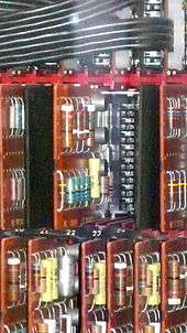
Transistor computers
Before transistors were invented, relays were used in early computers. The world's first working programmable, fully automatic digital computer,[253] the 1941 Z3 22-bit word length computer, had 2,600 relays, and operated at a clock frequency of about 4–5 Hz. The 1940 Complex Number Computer had fewer than 500 relays,[254] but it was not fully programmable.
The second generation of computers were transistor computers that featured boards filled with discrete transistors and magnetic memory cores. The experimental 1953 48-bit Transistor Computer, developed at the University of Manchester, is widely believed to be the first transistor computer to come into operation anywhere in the world (the prototype had 92 point-contact transistors and 550 diodes).[255] A later version the 1955 machine had a total of 250 junction transistors and 1300 point diodes. The Computer also used a small number of tubes in its clock generator, so it was not the first fully transistorized. The ETL Mark III, developed at the Electrotechnical Laboratory in 1956, may have been the first transistor-based electronic computer using the stored program method. It had about "130 point-contact transistors and about 1,800 germanium diodes were used for logic elements, and these were housed on 300 plug-in packages which could be slipped in and out.[256] The 1958 decimal architecture IBM 7070 was the first transistor computer to be fully programmable. It had about 30,000 alloy-junction germanium transistors and 22,000 germanium diodes, on approximately 14,000 Standard Modular System (SMS) cards. The 1959 MOBIDIC, short for "MOBIle DIgital Computer", at 12,000 pounds (6.0 short tons) mounted in the trailer of a semi-trailer truck, was a transistorized computer for battlefield data.
The third generation of computers used integrated circuits (ICs).[257] The 1962 15-bit Apollo Guidance Computer used "about 4,000 "Type-G" (3-input NOR gate) circuits" for about 12,000 transistors plus 32,000 resistors.[258] The first commercial IC-based computer was the IBM System/360 in 1964.[257] The 1965 12-bit PDP-8 CPU had 1409 transistors and over 10,000 diodes. It was not a microprocessor, as it used discrete transistors on many cards; but later microprocessors, such as the Intersil 6100 reimplemented it, see below.[259]
The next generation of computers were the microcomputers, also known as home computers or personal computers (PC), which used MOS microprocessors, in the 1970s. This list includes early transistorized computers (second generation) and IC-based computers (third generation) from the 1950s and 1960s.
| Computer | Transistor count | Year | Manufacturer | Notes | Ref |
|---|---|---|---|---|---|
| Transistor Computer | 92 | 1953 | University of Manchester | Point-contact transistors | [255] |
| TRADIC | 700 | 1954 | Bell Labs | Point-contact transistors | [255] |
| Transistor Computer (full size) | 250 | 1955 | University of Manchester | Discrete point-contact transistors | [255] |
| ETL Mark III | 130 | 1956 | Electrotechnical Laboratory | Point-contact transistors | [255][256] |
| Metrovick 950 | 200 | 1956 | Metropolitan-Vickers | Discrete junction transistors | |
| NEC NEAC-2201 | 600 | 1958 | NEC | Germanium transistors | [260] |
| Hitachi MARS-1 | 1,000 | 1958 | Hitachi | [261] | |
| IBM 7070 | 30,000 | 1958 | IBM | Alloy-junction germanium transistors | [262] |
| Matsushita MADIC-I | 400 | 1959 | Matsushita | Bipolar transistors | [263] |
| NEC NEAC-2203 | 2,579 | 1959 | NEC | [264] | |
| Toshiba TOSBAC-2100 | 5,000 | 1959 | Toshiba | [265] | |
| IBM 7090 | 50,000 | 1959 | IBM | Discrete germanium transistors | [266] |
| PDP-1 | 2,700 | 1959 | Digital Equipment Corporation | Discrete transistors | |
| Mitsubishi MELCOM 1101 | 3,500 | 1960 | Mitsubishi | Germanium transistors | [267] |
| M18 FADAC | 1,600 | 1960 | Autonetics | Discrete transistors | |
| D-17B | 1,521 | 1962 | Autonetics | Discrete transistors | |
| NEC NEAC-L2 | 16,000 | 1964 | NEC | Ge transistors | [268] |
| IBM System/360 | ? | 1964 | IBM | Integrated circuits | |
| PDP-8/I | 1409 | 1968 | Digital Equipment Corporation | 74 series TTL circuits | |
| Apollo Guidance Computer Block II | 12,300 | 1966 | Raytheon / MIT Instrumentation Laboratory | 4,100 ICs, each containing a 3-transistor, 3-input NOR gate |
Logic functions
Transistor count for generic logic functions is based on static CMOS implementation.[269]
| Function | Transistor count | Ref |
|---|---|---|
| NOT | 2 | |
| Buffer | 4 | |
| NAND 2-input | 4 | |
| NOR 2-input | 4 | |
| AND 2-input | 6 | |
| OR 2-input | 6 | |
| NAND 3-input | 6 | |
| NOR 3-input | 6 | |
| XOR 2-input | 6 | |
| XNOR 2-input | 8 | |
| MUX 2-input with TG | 6 | |
| MUX 4-input with TG | 18 | |
| NOT MUX 2-input | 8 | |
| MUX 4-input | 24 | |
| 1-bit adder full | 28 | |
| 1-bit adder–subtractor | 48 | |
| AND-OR-INVERT | 6 | [270] |
| Latch, D gated | 8 | |
| Flip-flop, edge triggered dynamic D with reset | 12 | |
| 8-bit multiplier | 3,000 | |
| 16-bit multiplier | 9,000 | |
| 32-bit multiplier | 21,000 | |
| small-scale integration | 2–100 | [271] |
| medium-scale integration | 100–500 | [271] |
| large-scale integration | 500–20,000 | [271] |
| very-large-scale integration | 20,000–1,000,000 | [271] |
| ultra-large scale integration | >1,000,000 |
Parallel systems
Historically, each processing element in earlier parallel systems—like all CPUs of that time—was a serial computer built out of multiple chips. As transistor counts per chip increases, each processing element could be built out of fewer chips, and then later each multi-core processor chip could contain more processing elements.[272]
Goodyear MPP: (1983?) 8 pixel processors per chip, 3,000 to 8,000 transistors per chip.[272]
Brunel University Scape (single-chip array-processing element): (1983) 256 pixel processors per chip, 120,000 to 140,000 transistors per chip.[272]
Cell Broadband Engine: (2006) with 9 cores per chip, had 234 million transistors per chip.[273]
Other devices
| Device type | Device name | Transistor count | Date of introduction | Designer(s) | Manufacturer(s) | MOS process | Area | Ref |
|---|---|---|---|---|---|---|---|---|
| Deep learning engine / IPU[lower-alpha 6] | Colossus GC2 | 23,600,000,000 | 2018 | Graphcore | TSMC | 16 nm | ~800 mm2 | [274][275][276] |
| Deep learning engine / IPU | Wafer Scale Engine | 1,200,000,000,000 | 2019 | Cerebras | TSMC | 16 nm | 46,225 mm2 | [5][6][7][8] |
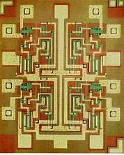
Transistor density
| Semiconductor device fabrication |
|---|
 |
|
(process nodes) |
The transistor density is the number of transistors that are fabricated per unit area, typically measured in terms of the number of transistors per square millimeter (mm2). The transistor density usually correlates with the gate length of a semiconductor node (also known as a semiconductor manufacturing process), typically measured in nanometers (nm). As of 2019, the semiconductor node with the highest transistor density is TSMC's 5 nanometer node, with 171.3 million transistors per square millimeter.[277]
MOSFET nodes
| Node name | Transistor density (transistors/mm2) | Production year | Process | MOSFET | Manufacturer(s) | Ref |
|---|---|---|---|---|---|---|
| ? | ? | 1960 | 20,000 nm | PMOS | Bell Labs | [278][279] |
| ? | ? | 1960 | 20,000 nm | NMOS | ||
| ? | ? | 1963 | ? | CMOS | Fairchild | [18] |
| ? | ? | 1964 | ? | PMOS | General Microelectronics | [280] |
| ? | ? | 1968 | 20,000 nm | CMOS | RCA | [281] |
| ? | ? | 1969 | 12,000 nm | PMOS | Intel | [214][206] |
| ? | ? | 1970 | 10,000 nm | CMOS | RCA | [281] |
| ? | 300 | 1970 | 8,000 nm | PMOS | Intel | [208][196] |
| ? | ? | 1971 | 10,000 nm | PMOS | Intel | [282] |
| ? | 480 | 1971 | ? | PMOS | General Instrument | [210] |
| ? | ? | 1973 | ? | NMOS | Texas Instruments | [210] |
| ? | 220 | 1973 | ? | NMOS | Mostek | [210] |
| ? | ? | 1973 | 7,500 nm | NMOS | NEC | [25][24] |
| ? | ? | 1973 | 6,000 nm | PMOS | Toshiba | [26][283] |
| ? | ? | 1976 | 5,000 nm | NMOS | Hitachi, Intel | [210] |
| ? | ? | 1976 | 5,000 nm | CMOS | RCA | |
| ? | ? | 1976 | 4,000 nm | NMOS | Zilog | |
| ? | ? | 1976 | 3,000 nm | NMOS | Intel | [284] |
| ? | 1,850 | 1977 | ? | NMOS | NTT | [210] |
| ? | ? | 1978 | 3,000 nm | CMOS | Hitachi | [285] |
| ? | ? | 1978 | 2,500 nm | NMOS | Texas Instruments | [210] |
| ? | ? | 1978 | 2,000 nm | NMOS | NEC, NTT | |
| ? | 2,600 | 1979 | ? | VMOS | Siemens | |
| ? | 7,280 | 1979 | 1,000 nm | NMOS | NTT | |
| ? | 7,620 | 1980 | 1,000 nm | NMOS | NTT | |
| ? | ? | 1983 | 2,000 nm | CMOS | Toshiba | [214] |
| ? | ? | 1983 | 1,500 nm | CMOS | Intel | [210] |
| ? | ? | 1983 | 1,200 nm | CMOS | Intel | |
| ? | ? | 1984 | 800 nm | CMOS | NTT | |
| ? | ? | 1987 | 700 nm | CMOS | Fujitsu | |
| ? | ? | 1989 | 600 nm | CMOS | Mitsubishi, NEC, Toshiba | [214] |
| ? | ? | 1989 | 500 nm | CMOS | Hitachi, Mitsubishi, NEC, Toshiba | |
| ? | ? | 1991 | 400 nm | CMOS | Matsushita, Mitsubishi, Fujitsu, Toshiba | |
| ? | ? | 1993 | 350 nm | CMOS | Sony | |
| ? | ? | 1993 | 250 nm | CMOS | Hitachi, NEC | |
| 3LM | 32,000 | 1994 | 350 nm | CMOS | NEC | [136] |
| ? | ? | 1995 | 160 nm | CMOS | Hitachi | [214] |
| ? | ? | 1996 | 150 nm | CMOS | Mitsubishi | |
| TSMC 180 nm | ? | 1998 | 180 nm | CMOS | TSMC | [286] |
| CS80 | ? | 1999 | 180 nm | CMOS | Fujitsu | [287] |
| ? | ? | 1999 | 180 nm | CMOS | Intel, Sony, Toshiba | [204][61] |
| CS85 | ? | 1999 | 170 nm | CMOS | Fujitsu | [288] |
| Samsung 140 nm | ? | 1999 | 140 nm | CMOS | Samsung | [214] |
| ? | ? | 2001 | 130 nm | CMOS | Fujitsu, Intel | [287][204] |
| Samsung 100 nm | ? | 2001 | 100 nm | CMOS | Samsung | [214] |
| ? | ? | 2002 | 90 nm | CMOS | Sony, Toshiba, Samsung | [61][232] |
| CS100 | ? | 2003 | 90 nm | CMOS | Fujitsu | [287] |
| Intel 90 nm | 1,450,000 | 2004 | 90 nm | CMOS | Intel | [289][204] |
| Samsung 80 nm | ? | 2004 | 80 nm | CMOS | Samsung | [290] |
| ? | ? | 2004 | 65 nm | CMOS | Fujitsu, Toshiba | [291] |
| Samsung 60 nm | ? | 2004 | 60 nm | CMOS | Samsung | [232] |
| TSMC 45 nm | ? | 2004 | 45 nm | CMOS | TSMC | |
| Elpida 90 nm | ? | 2005 | 90 nm | CMOS | Elpida Memory | [292] |
| CS200 | ? | 2005 | 65 nm | CMOS | Fujitsu | [293][287] |
| Samsung 50 nm | ? | 2005 | 50 nm | CMOS | Samsung | [234] |
| Intel 65 nm | 2,080,000 | 2006 | 65 nm | CMOS | Intel | [289] |
| Samsung 40 nm | ? | 2006 | 40 nm | CMOS | Samsung | [234] |
| Toshiba 56 nm | ? | 2007 | 56 nm | CMOS | Toshiba | [235] |
| Matsushita 45 nm | ? | 2007 | 45 nm | CMOS | Matsushita | [71] |
| Intel 45 nm | 3,300,000 | 2008 | 45 nm | CMOS | Intel | [294] |
| Toshiba 43 nm | ? | 2008 | 43 nm | CMOS | Toshiba | [236] |
| TSMC 40 nm | ? | 2008 | 40 nm | CMOS | TSMC | [295] |
| Toshiba 32 nm | ? | 2009 | 32 nm | CMOS | Toshiba | [296] |
| Intel 32 nm | 7,500,000 | 2010 | 32 nm | CMOS | Intel | [294] |
| ? | ? | 2010 | 20 nm | CMOS | Hynix, Samsung | [297][234] |
| Intel 22 nm | 15,300,000 | 2012 | 22 nm | CMOS | Intel | [294] |
| IMFT 20 nm | ? | 2012 | 20 nm | CMOS | IMFT | [298] |
| Toshiba 19 nm | ? | 2012 | 19 nm | CMOS | Toshiba | |
| Hynix 16 nm | ? | 2013 | 16 nm | FinFET | SK Hynix | [297] |
| TSMC 16 nm | 28,880,000 | 2013 | 16 nm | FinFET | TSMC | [299][300] |
| Samsung 10 nm | 51,820,000 | 2013 | 10 nm | FinFET | Samsung | [301][302] |
| Intel 14 nm | 37,500,000 | 2014 | 14 nm | FinFET | Intel | [294] |
| 14LP | 32,940,000 | 2015 | 14 nm | FinFET | Samsung | [301] |
| TSMC 10 nm | 52,510,000 | 2016 | 10 nm | FinFET | TSMC | [299][303] |
| 12LP | 36,710,000 | 2017 | 12 nm | FinFET | GlobalFoundries, Samsung | [163] |
| N7FF | 96,500,000 | 2017 | 7 nm | FinFET | TSMC | [304][305][306] |
| 8LPP | 61,180,000 | 2018 | 8 nm | FinFET | Samsung | [301] |
| 7LPE | 95,300,000 | 2018 | 7 nm | FinFET | Samsung | [305] |
| Intel 10 nm | 100,760,000 | 2018 | 10 nm | FinFET | Intel | [307] |
| 5LPE | 126,530,000 | 2018 | 5 nm | FinFET | Samsung | [308][309] |
| N7FF+ | 113,900,000 | 2019 | 7 nm | FinFET | TSMC | [304][305] |
| CLN5FF | 171,300,000 | 2019 | 5 nm | FinFET | TSMC | [277] |
| TSMC 3 nm | ? | ? | 3 nm | ? | TSMC | [310] |
| Samsung 3 nm | ? | ? | 3 nm | GAAFET | Samsung | [311] |
See also
- Gate count, an alternate metric
- Dennard scaling
- Electronics industry
- Integrated circuit
- List of best-selling electronic devices
- List of semiconductor scale examples
- MOSFET
- Semiconductor
- Semiconductor device
- Semiconductor device fabrication
- Semiconductor industry
- Transistor
Notes
- Declassified 1998
- 3,510 without depletion mode pull-up transistors
- 6,813 without depletion mode pull-up transistors
- 3,900,000,000 core chiplet die, 2,090,000,000 I/O die
- Estimate
- "Intelligence Processing Unit"
References
- Broekhuijsen, Niels (October 23, 2019). "AMD's 64-Core EPYC and Ryzen CPUs Stripped: A Detailed Inside Look". Retrieved October 24, 2019.
- Mujtaba, Hassan (October 22, 2019). "AMD 2nd Gen EPYC Rome Processors Feature A Gargantuan 39.54 Billion Transistors, IO Die Pictured in Detail". Retrieved October 24, 2019.
- Walton, Jared (May 14, 2020). "Nvidia Unveils Its Next-Generation 7nm Ampere A100 GPU for Data Centers, and It's Absolutely Massive". Tom's Hardware.
- Manners, David (January 30, 2019). "Samsung makes 1TB flash eUFS module". Electronics Weekly. Retrieved June 23, 2019.
- Hruska, Joel (August 2019). "Cerebras Systems Unveils 1.2 Trillion Transistor Wafer-Scale Processor for AI". extremetech.com. Retrieved September 6, 2019.
- Feldman, Michael (August 2019). "Machine Learning chip breaks new ground with waferscale integration". nextplatform.com. Retrieved September 6, 2019.
- Cutress, Ian (August 2019). "Hot Chips 31 Live Blogs: Cerebras' 1.2 Trillion Transistor Deep Learning Processor". anandtech.com. Retrieved September 6, 2019.
- "A Look at Cerebras Wafer-Scale Engine: Half Square Foot Silicon Chip". WikiChip Fuse. November 16, 2019. Retrieved December 2, 2019.
- "John Gustafson's answer to How many individual transistors are in the world's most powerful supercomputer?". Quora. Retrieved August 22, 2019.
- "13 Sextillion & Counting: The Long & Winding Road to the Most Frequently Manufactured Human Artifact in History". Computer History Museum. April 2, 2018. Retrieved July 28, 2019.
- Moskowitz, Sanford L. (2016). Advanced Materials Innovation: Managing Global Technology in the 21st century. John Wiley & Sons. pp. 165–168. ISBN 9780470508923.
- "1960 - Metal Oxide Semiconductor (MOS) Transistor Demonstrated". The Silicon Engine. Computer History Museum.
- "Who Invented the Transistor?". Computer History Museum. December 4, 2013. Retrieved July 20, 2019.
- "Transistors Keep Moore's Law Alive". EETimes. December 12, 2018. Retrieved July 18, 2019.
- "Tortoise of Transistors Wins the Race – CHM Revolution". Computer History Museum. Retrieved July 22, 2019.
- Hittinger, William C. (1973). "Metal-Oxide-Semiconductor Technology". Scientific American. 229 (2): 48–59. Bibcode:1973SciAm.229b..48H. doi:10.1038/scientificamerican0873-48. ISSN 0036-8733. JSTOR 24923169.
- Bassett, Ross Knox (2007). To the Digital Age: Research Labs, Start-up Companies, and the Rise of MOS Technology. Johns Hopkins University Press. p. 22. ISBN 9780801886393.
- "1963: Complementary MOS Circuit Configuration is Invented". Computer History Museum. Retrieved July 6, 2019.
- "1971: Microprocessor Integrates CPU Function onto a Single Chip". The Silicon Engine. Computer History Museum. Retrieved September 4, 2019.
- Holt, Ray. "World's First Microprocessor". Retrieved March 5, 2016.
1st fully integrated chip set microprocessor
- "Alpha 21364 - Microarchitectures - Compaq - WikiChip". en.wikichip.org. Retrieved September 8, 2019.
- Ken Shirriff. "The Texas Instruments TMX 1795: the (almost) first, forgotten microprocessor". 2015.
- Ryoichi Mori; Hiroaki Tajima; Morihiko Tajima; Yoshikuni Okada (October 1977). "Microprocessors in Japan". Euromicro Newsletter. 3 (4): 50–7. doi:10.1016/0303-1268(77)90111-0.
- "NEC 751 (uCOM-4)". The Antique Chip Collector's Page. Archived from the original on May 25, 2011. Retrieved June 11, 2010.
- "1970s: Development and evolution of microprocessors" (PDF). Semiconductor History Museum of Japan. Retrieved June 27, 2019.
- "1973: 12-bit engine-control microprocessor (Toshiba)" (PDF). Semiconductor History Museum of Japan. Retrieved June 27, 2019.
- "Low Bandwidth Timeline – Semiconductor". Texas Instruments. Retrieved June 22, 2016.
- "The MOS 6502 and the Best Layout Guy in the World". research.swtch.com. January 3, 2011. Retrieved September 3, 2019.
- "Digital History: ZILOG Z8000 (APRIL 1979)". OLD-COMPUTERS.COM : The Museum. Retrieved June 19, 2019.
- "Chip Hall of Fame: Motorola MC68000 Microprocessor". IEEE Spectrum. Institute of Electrical and Electronics Engineers. June 30, 2017. Retrieved June 19, 2019.
- Microprocessors: 1971 to 1976 Christiansen
- "Microprocessors 1976 to 1981". weber.edu. Retrieved August 9, 2014.
- "W65C816S 16-bit Core". www.westerndesigncenter.com. Retrieved September 12, 2017.
- Demone, Paul (November 9, 2000). "ARM's Race to World Domination". real world technologies. Retrieved July 20, 2015.
- Hand, Tom. "The Harris RTX 2000 Microcontroller" (PDF). mpeforth.com. Retrieved August 9, 2014.
- "Forth chips list". UltraTechnology. March 15, 2001. Retrieved August 9, 2014.
- Koopman, Philip J. (1989). "4.4 Architecture of the Novix NC4016". Stack Computers: the new wave. Ellis Horwood Series in Computers and Their Applications. Carnegie Mellon University. ISBN 978-0745804187. Retrieved August 9, 2014.
- "Fujitsu SPARC". cpu-collection.de. Retrieved June 30, 2019.
- Kimura S, Komoto Y, Yano Y (1988). "Implementation of the V60/V70 and its FRM function". IEEE Micro. 8 (2): 22–36. doi:10.1109/40.527.
- "VL2333 - VTI - WikiChip". en.wikichip.org. Retrieved August 31, 2019.
- Inayoshi H, Kawasaki I, Nishimukai T, Sakamura K (1988). "Realization of Gmicro/200". IEEE Micro. 8 (2): 12–21. doi:10.1109/40.526.
- Bosshart, P.; Hewes, C.; Mi-Chang Chang; Kwok-Kit Chau; Hoac, C.; Houston, T.; Kalyan, V.; Lusky, S.; Mahant-Shetti, S.; Matzke, D.; Ruparel, K.; Ching-Hao Shaw; Sridhar, T.; Stark, D. (October 1987). "A 553K-Transistor LISP Processor Chip". IEEE Journal of Solid-State Circuits. 22 (5): 202–3. doi:10.1109/ISSCC.1987.1157084.
- Fahlén, Lennart E.; Stockholm International Peace Research Institute (1987). "3. Hardware requirements for artificial intelligence § Lisp Machines: TI Explorer". Arms and Artificial Intelligence: Weapon and Arms Control Applications of Advanced Computing. SIPRI Monograph Series. Oxford University Press. p. 57. ISBN 978-0-19-829122-0.
- Jouppi, Norman P.; Tang, Jeffrey Y. F. (July 1989). "A 20-MIPS Sustained 32-bit CMOS Microprocessor with High Ratio of Sustained to Peak Performance". IEEE Journal of Solid-State Circuits. 24 (5): i. Bibcode:1989IJSSC..24.1348J. CiteSeerX 10.1.1.85.988. doi:10.1109/JSSC.1989.572612. WRL Research Report 89/11.
- "The CPU shack museum". CPUshack.com. May 15, 2005. Retrieved August 9, 2014.
- "Intel i960 Embedded Microprocessor". National High Magnetic Field Laboratory. Florida State University. March 3, 2003. Retrieved June 29, 2019.
- Venkatasawmy, Rama (2013). The Digitization of Cinematic Visual Effects: Hollywood's Coming of Age. Rowman & Littlefield. p. 198. ISBN 9780739176214.
- "SH Microprocessor Leading the Nomadic Era" (PDF). Semiconductor History Museum of Japan. Retrieved June 27, 2019.
- "SH2: A Low Power RISC Micro for Consumer Applications" (PDF). Hitachi. Retrieved June 27, 2019.
- "HARP-1: A 120 MHz Superscalar PA-RISC Processor" (PDF). Hitachi. Retrieved June 19, 2019.
- "ARM7 Statistics". Poppyfields.net. May 27, 1994. Retrieved August 9, 2014.
- "Forth Multiprocessor Chip MuP21". www.ultratechnology.com. Retrieved September 6, 2019.
MuP21 has a 21-bit CPU core, a memory coprocessor, and a video coprocessor
- "F21 CPU". www.ultratechnology.com. Retrieved September 6, 2019.
F21 offers video I/O, analog I/O, serial network I/O, and a parallel I/O port on chip. F21 has a transistor count of about 15,000 vs about 7,000 for MuP21.
- "Intel Pentium Pro 180". hw-museum.cz. Retrieved September 8, 2019.
- "PC Guide Intel Pentium Pro ("P6")". PCGuide.com. April 17, 2001. Retrieved August 9, 2014.
- "Remembering the Sega Dreamcast". Bit-Tech. September 29, 2009. Retrieved June 18, 2019.
- "Entertainment Systems and High-Performance Processor SH-4" (PDF). Hitachi Review. Hitachi. 48 (2): 58–63. 1999. Retrieved June 27, 2019.
- Hagiwara, Shiro; Oliver, Ian (November–December 1999). "Sega Dreamcast: Creating a Unified Entertainment World". IEEE Micro. IEEE Computer Society. 19 (6): 29–35. doi:10.1109/40.809375. Retrieved June 27, 2019.
- Ulf Samuelsson. "Transistor count of common uCs?". www.embeddedrelated.com. Retrieved September 8, 2019.
IIRC, The AVR core is 12,000 gates, and the megaAVR core is 20,000 gates. Each gate is 4 transistors. The chip is considerably larger since the memory uses quite a lot.
- Hennessy, John L.; Patterson, David A. (May 29, 2002). Computer Architecture: A Quantitative Approach (3 ed.). Morgan Kaufmann. p. 491. ISBN 978-0-08-050252-6. Retrieved April 9, 2013.
- "EMOTION ENGINE® AND GRAPHICS SYNTHESIZER USED IN THE CORE OF PLAYSTATION® BECOME ONE CHIP" (PDF). Sony. April 21, 2003. Retrieved June 26, 2019.
- Diefendorff, Keith (April 19, 1999). "Sony's Emotionally Charged Chip: Killer Floating-Point "Emotion Engine" To Power PlayStation 2000" (PDF). Microprocessor Report. 13 (5). Retrieved June 19, 2019.
- "NVIDIA GeForce 7800 GTX GPU Review". PC Perspective. June 22, 2005. Retrieved June 18, 2019.
- Ando, H.; Yoshida, Y.; Inoue, A.; Sugiyama, I.; Asakawa, T.; Morita, K.; Muta, T.; otokurumada, T.; Okada, S.; Yamashita, H.; Satsukawa, Y.; Konmoto, A.; Yamashita, R.; Sugiyama, H. (2003). A 1.3GHz fifth eneration SPARC64 microprocessor. Design Automation Conference. pp. 702–705. doi:10.1145/775832.776010. ISBN 1-58113-688-9.
- Krewell, Kevin (21 October 2002). "Fujitsu's SPARC64 V Is Real Deal". Microprocessor Report.
- Fujitsu Limited (August 2004). SPARC64 V Processor For UNIX Server.
- "A Glimpse Inside The Cell Processor". Gamasutra. July 13, 2006. Retrieved June 19, 2019.
- "PRESS KIT — Dual-core Intel Itanium Processor". Intel. Retrieved August 9, 2014.
- Toepelt, Bert (January 8, 2009). "AMD Phenom II X4: 45nm Benchmarked — The Phenom II And AMD's Dragon Platform". TomsHardware.com. Retrieved August 9, 2014.
- "ARM (Advanced RISC Machines) Processors". EngineersGarage.com. Retrieved August 9, 2014.
- "Panasonic starts to sell a New-generation UniPhier System LSI". Panasonic. October 10, 2007. Retrieved July 2, 2019.
- "SPARC64 VI Extensions" page 56, Fujitsu Limited, Release 1.3, 27 March 2007
- Morgan, Timothy Prickett (17 July 2008). "Fujitsu and Sun Flex Their Quads with New Sparc Server Lineup". The Unix Guardian, Vol. 8, No. 27.
- Takumi Maruyama (2009). SPARC64 VIIIfx: Fujitsu's New Generation Octo Core Processor for PETA Scale computing (PDF). Proceedings of Hot Chips 21. IEEE Computer Society. Archived from the original (PDF) on October 8, 2010. Retrieved June 30, 2019.
- Stokes, Jon (February 10, 2010). "Sun's 1 billion-transistor, 16-core Niagara 3 processor". ArsTechnica.com. Retrieved August 9, 2014.
- "IBM to Ship World's Fastest Microprocessor". IBM. September 1, 2010. Retrieved August 9, 2014.
- "Intel to deliver first computer chip with two billion transistors". AFP. February 5, 2008. Archived from the original on May 20, 2011. Retrieved February 5, 2008.
- "Intel Previews Intel Xeon 'Nehalem-EX' Processor." May 26, 2009. Retrieved on May 28, 2009.
- Morgan, Timothy Prickett (November 21, 2011), "Fujitsu parades 16-core Sparc64 super stunner", The Register, retrieved December 8, 2011
- Angelini, Chris (November 14, 2011). "Intel Core i7-3960X Review: Sandy Bridge-E And X79 Express". TomsHardware.com. Retrieved August 9, 2014.
- "IDF2012 Mark Bohr, Intel Senior Fellow" (PDF).
- "Images of SPARC64" (PDF). fujitsu.com. Retrieved August 29, 2017.
- "Intel's Atom Architecture: The Journey Begins". AnandTech. Retrieved April 4, 2010.
- "Intel Xeon Phi SE10X". TechPowerUp. Retrieved July 20, 2015.
- Shimpi, Lal. "The Haswell Review: Intel Core i7-4770K & i5-4670K Tested". anandtech. Retrieved November 20, 2014.
- "Dimmick, Frank (August 29, 2014). "Intel Core i7 5960X Extreme Edition Review". Overclockers Club. Retrieved August 29, 2014.
- "Apple A8X". NotebookCheck. Retrieved July 20, 2015.
- "Intel Readying 15-core Xeon E7 v2". AnandTech. Retrieved August 9, 2014.
- "Intel Xeon E5-2600 v3 Processor Overview: Haswell-EP Up to 18 Cores". pcper. Retrieved January 29, 2015.
- "Intel's Broadwell-U arrives aboard 15W, 28W mobile processors". TechReport. Retrieved January 5, 2015.
- http://www.enterprisetech.com/2014/08/13/oracle-cranks-cores-32-sparc-m7-chip/
- "Qualcomm Snapdragon 835 (8998)". NotebookCheck. Retrieved September 23, 2017.
- Takahashi, Dean (January 3, 2017). "Qualcomm's Snapdragon 835 will debut with 3 billion transistors and a 10nm manufacturing process". VentureBeat.
- "Broadwell-E: Intel Core i7-6950X, 6900K, 6850K & 6800K Review". Tom's Hardware. May 30, 2016. Retrieved April 12, 2017.
- "The Broadwell-E Review". PC Gamer. July 8, 2016. Retrieved April 12, 2017.
- "HUAWEI TO UNVEIL KIRIN 970 SOC WITH AI UNIT, 5.5 BILLION TRANSISTORS AND 1.2 GBPS LTE SPEED AT IFA 2017". firstpost.com. September 1, 2017. Retrieved November 18, 2018.
- "Broadwell-EP Architecture - Intel Xeon E5-2600 v4 Broadwell-EP Review". Tom's Hardware. March 31, 2016. Retrieved April 4, 2016.
- "About the ZipCPU". zipcpu.com. Retrieved September 10, 2019.
As of ORCONF, 2016, the ZipCPU used between 1286 and 4926 6-LUTs, depending upon how it is configured.
- "Qualcomm Snapdragon 1000 for laptops could pack 8.5 billion transistors". techradar. Retrieved September 23, 2017.
- "Spotted: Qualcomm Snapdragon 8cx Wafer on 7nm". AnandTech. Retrieved December 6, 2018.
- Cutress, Ian (February 22, 2017). "AMD Launches Zen". Anandtech.com. Retrieved February 22, 2017.
- "Ryzen 5 1600 - AMD". Wikichip.org. April 20, 2018. Retrieved December 9, 2018.
- "Ryzen 5 1600X – AMD". Wikichip.org. October 26, 2018. Retrieved December 9, 2018.
- "Kirin 970 – HiSilicon". Wikichip. March 1, 2018. Retrieved November 8, 2018.
- Leadbetter, Richard (April 6, 2017). "Inside the next Xbox: Project Scorpio tech revealed". Eurogamer. Retrieved May 3, 2017.
- "Intel Xeon Platinum 8180". TechPowerUp. December 1, 2018. Retrieved December 2, 2018.
- Lee, Y. "SiFive Freedom SoCs : Industry's First Open Source RISC V Chips" (PDF). HotChips 29 IOT/Embedded.
- "Documents at Fujitsu" (PDF). fujitsu.com. Retrieved August 29, 2017.
- Schmerer, Kai (November 5, 2018). "iPad Pro 2018: A12X-Prozessor bietet deutlich mehr Leistung". ZDNet.de (in German).
- "Qualcomm Datacenter Technologies Announces Commercial Shipment of Qualcomm Centriq 2400 – The World's First 10nm Server Processor and Highest Performance Arm-based Server Processor Family Ever Designed". Qualcomm. Retrieved November 9, 2017.
- "Qualcomm Snapdragon 8180: 7nm SoC SDM1000 With 8.5 Billion Transistors To Challenge Apple A12 Bionic Chipset". dailyhunt. Retrieved September 21, 2018.
- Yang, Daniel; Wegner, Stacy (September 21, 2018). "Apple iPhone Xs Max Teardown". TechInsights. Retrieved September 21, 2018.
- "Apple's A12 Bionic is the first 7-nanometer smartphone chip". Engadget. Retrieved September 26, 2018.
- "Kirin 980 – HiSilicon". Wikichip. November 8, 2018. Retrieved November 8, 2018.
- Friedman, Alan. "5nm Kirin 1020 SoC tipped for next year's Huawei Mate 40 line". Phone Arena. Retrieved December 23, 2019.
- Frumusanu, Andrei. "The Huawei Mate 30 Pro Review: Top Hardware without Google?". AnandTech. Retrieved January 2, 2020.
- "HiSilicon Kirin 710". Notebookcheck. September 19, 2018. Retrieved November 24, 2018.
- Zafar, Ramish (October 30, 2018). "Apple's A12X Has 10 Billion Transistors, 90% Performance Boost & 7-Core GPU". Wccftech.
- Zafar, Ramish (September 10, 2019). "Apple A13 For iPhone 11 Has 8.5 Billion Transistors, Quad-Core GPU". Wccftech. Retrieved September 11, 2019.
- Introducing iPhone 11 Pro — Apple Youtube Video, retrieved September 11, 2019
- "Fujitsu began to produce Japan's billions of super-calculations with the strongest ARM processor A64FX". firstxw.com. April 16, 2019. Retrieved June 19, 2019.
- "Fujitsu Successfully Triples the Power Output of Gallium-Nitride Transistors". Fujitsu. August 22, 2018. Retrieved June 19, 2019.
- "Hot Chips 30: Nvidia Xavier SoC". fuse.wikichip.org. September 18, 2018. Retrieved December 6, 2018.
- "AMD Ryzen 9 3900X and Ryzen 7 3700X Review: Zen 2 and 7nm Unleashed". Tom's Hardware. July 7, 2019. Retrieved October 19, 2019.
- CPUs, Arne Verheyde 2019-12-05T19:12:44Z. "Amazon Compares 64-core ARM Graviton2 to Intel's Xeon". Tom's Hardware. Retrieved December 6, 2019.
- Morgan, Timothy Prickett (December 3, 2019). "Finally: AWS Gives Servers A Real Shot In The Arm". The Next Platform. Retrieved December 6, 2019.
- Williams, Chris. "Nvidia's Tesla P100 has 15 billion transistors, 21TFLOPS". www.theregister.co.uk. Retrieved August 12, 2019.
- "Famous Graphics Chips: NEC µPD7220 Graphics Display Controller". IEEE Computer Society. Institute of Electrical and Electronics Engineers. August 22, 2018. Retrieved June 21, 2019.
- "GPU History: Hitachi ARTC HD63484. The second graphics processor". IEEE Computer Society. Institute of Electrical and Electronics Engineers. Retrieved June 21, 2019.
- "30 Years of Console Gaming". Klinger Photography. August 20, 2017. Retrieved June 19, 2019.
- "Sega Saturn". MAME. Retrieved July 18, 2019.
- "ASIC CHIPS ARE INDUSTRY'S GAME WINNERS". The Washington Post. September 18, 1995. Retrieved June 19, 2019.
- "Is it Time to Rename the GPU?". Jon Peddie Research. IEEE Computer Society. July 9, 2018. Retrieved June 19, 2019.
- "FastForward Sony Taps LSI Logic for PlayStation Video Game CPU Chip". FastForward. Retrieved January 29, 2014.
- "Reality Co-Processor − The Power In Nintendo64" (PDF). Silicon Graphics. August 26, 1997. Retrieved June 18, 2019.
- "Imagination PowerVR PCX2 GPU". VideoCardz.net. Retrieved June 19, 2019.
- Lilly, Paul (May 19, 2009). "From Voodoo to GeForce: The Awesome History of 3D Graphics". PC Gamer. Retrieved June 19, 2019.
- "3D accelerator database". Vintage 3D. Retrieved July 21, 2019.
- "RIVA128 Datasheet". SGS Thomson Microelectronics. Retrieved July 21, 2019.
- Singer, Graham (April 3, 2013). "History of the Modern Graphics Processor, Part 2". TechSpot. Retrieved July 21, 2019.
- Weinberg, Neil (September 7, 1998). "Comeback kid". Forbes. Retrieved June 19, 2019.
- Charles, Bertie (1998). "Sega's New Dimension". Forbes. Forbes Incorporated. 162 (5–9): 206.
The chip, etched in 0.25-micron detail — state-of-the-art for graphics processors — fits 10 million transistors
- "VideoLogic Neon 250 4MB". VideoCardz.net. Retrieved June 19, 2019.
- Shimpi, Anand Lal (November 21, 1998). "Fall Comdex '98 Coverage". AnandTech. Retrieved June 19, 2019.
- "NVIDIA NV10 A3 GPU Specs". TechPowerUp. Retrieved June 19, 2019.
- IGN Staff (November 4, 2000). "Gamecube Versus PlayStation 2". IGN. Retrieved November 22, 2015.
- "NVIDIA NV2A GPU Specs". TechPowerUp. Retrieved July 21, 2019.
- "ATI Xenos GPU Specs". TechPowerUp. Retrieved June 21, 2019.
- International, GamesIndustry (July 14, 2005). "TSMC to manufacture X360 GPU". Eurogamer. Retrieved August 22, 2006.
- "NVIDIA Playstation 3 RSX 65nm Specs". TechPowerUp. Retrieved June 21, 2019.
- "PS3 Graphics Chip Goes 65nm in Fall". Edge Online. June 26, 2008.
- "The Radeon HD 4850 & 4870: AMD Wins at $199 and $299". AnandTech.com. Retrieved August 9, 2014.
- "NVIDIA's 1.4 Billion Transistor GPU: GT200 Arrives as the GeForce GTX 280 & 260". AnandTech.com. Retrieved August 9, 2014.
- "Radeon 5870 specifications". AMD. Retrieved August 9, 2014.
- Glaskowsky, Peter. "ATI and Nvidia face off-obliquely". CNET. Retrieved August 9, 2014.
- Woligroski, Don (December 22, 2011). "AMD Radeon HD 7970". TomsHardware.com. Retrieved August 9, 2014.
- "Whitepaper: NVIDIA GeForce GTX 680" (PDF). NVIDIA. 2012. Archived from the original (PDF) on April 17, 2012.
- http://www.nvidia.com/content/PDF/kepler/NVIDIA-Kepler-GK110-Architecture-Whitepaper.pdf
- Smith, Ryan (November 12, 2012). "NVIDIA Launches Tesla K20 & K20X: GK110 Arrives At Last". AnandTech.
- "AMD Xbox One GPU". www.techpowerup.com. Retrieved February 5, 2020.
- "AMD PlayStation 4 GPU". www.techpowerup.com. Retrieved February 5, 2020.
- Schor, David (July 22, 2018). "VLSI 2018: GlobalFoundries 12nm Leading-Performance, 12LP". WikiChip Fuse. Retrieved May 31, 2019.
- "AMD Xbox One S GPU". www.techpowerup.com. Retrieved February 5, 2020.
- "AMD PlayStation 4 Pro GPU". www.techpowerup.com. Retrieved February 5, 2020.
- Smith, Ryan (June 29, 2016). "The AMD RX 480 Preview". Anandtech.com. Retrieved February 22, 2017.
- Harris, Mark (April 5, 2016). "Inside Pascal: NVIDIA's Newest Computing Platform". Nvidia developer blog.
- "AMD Xbox One X GPU". www.techpowerup.com. Retrieved February 5, 2020.
- "Radeon's next-generation Vega architecture" (PDF).
- Durant, Luke; Giroux, Olivier; Harris, Mark; Stam, Nick (May 10, 2017). "Inside Volta: The World's Most Advanced Data Center GPU". Nvidia developer blog.
- "NVIDIA TURING GPU ARCHITECTURE: Graphics Reinvented" (PDF). Nvidia. 2018. Retrieved June 28, 2019.
- "NVIDIA GeForce GTX 1660 Ti". www.techpowerup.com. Retrieved February 5, 2020.
- "NVIDIA GeForce GTX 1650". www.techpowerup.com. Retrieved February 5, 2020.
- "AMD Radeon RX 5500 XT". www.techpowerup.com. Retrieved February 5, 2020.
- "AMD Radeon RX 5700 XT". www.techpowerup.com. Retrieved February 5, 2020.
- "Nvidia Ampere Architecture". www.nvidia.com. Retrieved May 15, 2020.
- "Taiwan Company UMC Delivers 65nm FPGAs to Xilinx." SDA-ASIA Thursday, November 9, 2006.
- ""Altera's new 40nm FPGAs — 2.5 billion transistors!". pldesignline.com.
- "Altera unveils 28-nm Stratix V FPGA family". April 20, 2010. Retrieved April 20, 2010.
- "Design of a High-Density SoC FPGA at 20nm" (PDF). 2014. Retrieved July 16, 2017.
- Maxfield, Clive (October 2011). "New Xilinx Virtex-7 2000T FPGA provides equivalent of 20 million ASIC gates". EETimes. AspenCore. Retrieved September 4, 2019.
- Greenhill, D.; Ho, R.; Lewis, D.; Schmit, H.; Chan, K. H.; Tong, A.; Atsatt, S.; How, D.; McElheny, P. (February 2017). "3.3 A 14nm 1GHz FPGA with 2.5D transceiver integration". 2017 IEEE International Solid-State Circuits Conference (ISSCC): 54–55. doi:10.1109/ISSCC.2017.7870257. ISBN 978-1-5090-3758-2.
- "3.3 A 14nm 1GHz FPGA with 2.5D transceiver integration | DeepDyve". May 17, 2017. Archived from the original on May 17, 2017. Retrieved September 19, 2019.
- Santarini, Mike (May 2014). "Xilinx Ships Industry's First 20-nm All Programmable Devices" (PDF). Xcell journal. No. 86. Xilinx. p. 14. Retrieved June 3, 2014.
- Gianelli, Silvia (January 2015). "Xilinx Delivers the Industry's First 4M Logic Cell Device, Offering >50M Equivalent ASIC Gates and 4X More Capacity than Competitive Alternatives". www.xilinx.com. Retrieved August 22, 2019.
- Sims, Tara (August 2019). "Xilinx Announces the World's Largest FPGA Featuring 9 Million System Logic Cells". www.xilinx.com. Retrieved August 22, 2019.
- Verheyde, Arne (August 2019). "Xilinx Introduces World's Largest FPGA With 35 Billion Transistors". www.tomshardware.com. Retrieved August 23, 2019.
- Cutress, Ian (August 2019). "Xilinx Announces World Largest FPGA: Virtex Ultrascale+ VU19P with 9m Cells". www.anandtech.com. Retrieved September 25, 2019.
- Abazovic, Fuad (May 2019). "Xilinx 7nm Versal taped out last year". Retrieved September 30, 2019.
- Cutress, Ian (August 2019). "Hot Chips 31 Live Blogs: Xilinx Versal AI Engine". Retrieved September 30, 2019.
- Krewell, Kevin (August 2019). "Hot Chips 2019 highlights new AI strategies". Retrieved September 30, 2019.
- Leibson, Steven (November 6, 2019). "Intel announces Intel Stratix 10 GX 10M FPGA, worlds highest capacity with 10.2 million logic elements". Retrieved November 7, 2019.
- Verheyde, Arne (November 6, 2019). "Intel Introduces World's Largest FPGA With 43.3 Billion Transistors". Retrieved November 7, 2019.
- The DRAM memory of Robert Dennard history-computer.com
- "Late 1960s: Beginnings of MOS memory" (PDF). Semiconductor History Museum of Japan. January 23, 2019. Retrieved June 27, 2019.
- "1970: Semiconductors compete with magnetic cores". Computer History Museum. Retrieved June 19, 2019.
- "2.1.1 Flash Memory". TU Wien. Retrieved June 20, 2019.
- Shilov, Anton. "SK Hynix Starts Production of 128-Layer 4D NAND, 176-Layer Being Developed". www.anandtech.com. Retrieved September 16, 2019.
- "Samsung Begins Production of 100+ Layer Sixth-Generation V-NAND Flash". PC Perspective. August 11, 2019. Retrieved September 16, 2019.
- "1966: Semiconductor RAMs Serve High-speed Storage Needs". Computer History Museum. Retrieved June 19, 2019.
- "Specifications for Toshiba "TOSCAL" BC-1411". Old Calculator Web Museum. Archived from the original on July 3, 2017. Retrieved May 8, 2018.
- "Toshiba "Toscal" BC-1411 Desktop Calculator". Old Calculator Web Museum. Archived from the original on May 20, 2007.
- "IBM first in IC memory". Computer History Museum. Retrieved June 19, 2019.
- "A chronological list of Intel products. The products are sorted by date" (PDF). Intel museum. Intel Corporation. July 2005. Archived from the original (PDF) on August 9, 2007. Retrieved July 31, 2007.
- "1970s: SRAM evolution" (PDF). Semiconductor History Museum of Japan. Retrieved June 27, 2019.
- Pimbley, J. (2012). Advanced CMOS Process Technology. Elsevier. p. 7. ISBN 9780323156806.
- "Intel: 35 Years of Innovation (1968–2003)" (PDF). Intel. 2003. Retrieved June 26, 2019.
- Lojek, Bo (2007). History of Semiconductor Engineering. Springer Science & Business Media. pp. 362–363. ISBN 9783540342588.
The i1103 was manufactured on a 6-mask silicon-gate P-MOS process with 8 μm minimum features. The resulting product had a 2,400 µm2 memory cell size, a die size just under 10 mm2, and sold for around $21.
- "Manufacturers in Japan enter the DRAM market and integration densities are improved" (PDF). Semiconductor History Museum of Japan. Retrieved June 27, 2019.
- Gealow, Jeffrey Carl (August 10, 1990). "Impact of Processing Technology on DRAM Sense Amplifier Design" (PDF). CORE. Massachusetts Institute of Technology. pp. 149–166. Retrieved June 25, 2019.
- "Silicon Gate MOS 2102A". Intel. Retrieved June 27, 2019.
- "One of the Most Successful 16K Dynamic RAMs: The 4116". National Museum of American History. Smithsonian Institution. Retrieved June 20, 2019.
- Component Data Catalog (PDF). Intel. 1978. pp. 3–94. Retrieved June 27, 2019.
- "Memory". STOL (Semiconductor Technology Online). Retrieved June 25, 2019.
- "The Cutting Edge of IC Technology: The First 294,912-Bit (288K) Dynamic RAM". National Museum of American History. Smithsonian Institution. Retrieved June 20, 2019.
- "Computer History for 1984". Computer Hope. Retrieved June 25, 2019.
- "Japanese Technical Abstracts". Japanese Technical Abstracts. University Microfilms. 2 (3–4): 161. 1987.
The announcement of 1M DRAM in 1984 began the era of megabytes.
- "KM48SL2000-7 Datasheet". Samsung. August 1992. Retrieved June 19, 2019.
- "Electronic Design". Electronic Design. Hayden Publishing Company. 41 (15–21). 1993.
The first commercial synchronous DRAM, the Samsung 16-Mbit KM48SL2000, employs a single-bank architecture that lets system designers easily transition from asynchronous to synchronous systems.
- Breaking the gigabit barrier, DRAMs at ISSCC portend major system-design impact. (dynamic random access memory; International Solid-State Circuits Conference; Hitachi Ltd. and NEC Corp. research and development) Highbeam Business, January 9, 1995
- "Japanese Company Profiles" (PDF). Smithsonian Institution. 1996. Retrieved June 27, 2019.
- "History: 1990s". SK Hynix. Retrieved July 6, 2019.
- "Samsung 50nm 2GB DDR3 chips are industry's smallest". SlashGear. September 29, 2008. Retrieved June 25, 2019.
- Shilov, Anton (July 19, 2017). "Samsung Increases Production Volumes of 8 GB HBM2 Chips Due to Growing Demand". AnandTech. Retrieved June 29, 2019.
- "Samsung Unleashes a Roomy DDR4 256GB RAM". Tom's Hardware. September 6, 2018. Retrieved June 21, 2019.
- "First 3D Nanotube and RRAM ICs Come Out of Foundry". IEEE Spectrum: Technology, Engineering, and Science News. July 19, 2019. Retrieved September 16, 2019.
This wafer was made just last Friday… and it's the first monolithic 3D IC ever fabricated within a foundry
- "Three Dimensional Monolithic System-on-a-Chip". www.darpa.mil. Retrieved September 16, 2019.
- "DARPA 3DSoC Initiative Completes First Year, Update Provided at ERI Summit on Key Steps Achieved to Transfer Technology into SkyWater's 200mm U.S. Foundry". Skywater Technology Foundry (Press release). July 25, 2019. Retrieved September 16, 2019.
- "DD28F032SA Datasheet". Intel. Retrieved June 27, 2019.
- "TOSHIBA ANNOUNCES 0.13 MICRON 1Gb MONOLITHIC NAND FEATURING LARGE BLOCK SIZE FOR IMPROVED WRITE/ERASE SPEED PERFORMANCE". Toshiba. September 9, 2002. Retrieved March 11, 2006.
- "TOSHIBA AND SANDISK INTRODUCE A ONE GIGABIT NAND FLASH MEMORY CHIP, DOUBLING CAPACITY OF FUTURE FLASH PRODUCTS". Toshiba. November 12, 2001. Retrieved June 20, 2019.
- "Our Proud Heritage from 2000 to 2009". Samsung Semiconductor. Samsung. Retrieved June 25, 2019.
- "TOSHIBA ANNOUNCES 1 GIGABYTE COMPACTFLASH™CARD". Toshiba. September 9, 2002. Retrieved March 11, 2006.
- "History". Samsung Electronics. Samsung. Retrieved June 19, 2019.
- "TOSHIBA COMMERCIALIZES INDUSTRY'S HIGHEST CAPACITY EMBEDDED NAND FLASH MEMORY FOR MOBILE CONSUMER PRODUCTS". Toshiba. April 17, 2007. Retrieved November 23, 2010.
- "Toshiba Launches the Largest Density Embedded NAND Flash Memory Devices". Toshiba. August 7, 2008. Retrieved June 21, 2019.
- "Toshiba Launches Industry's Largest Embedded NAND Flash Memory Modules". Toshiba. June 17, 2010. Retrieved June 21, 2019.
- "Samsung e·MMC Product family" (PDF). Samsung Electronics. December 2011. Retrieved July 15, 2019.
- Shilov, Anton (December 5, 2017). "Samsung Starts Production of 512 GB UFS NAND Flash Memory: 64-Layer V-NAND, 860 MB/s Reads". AnandTech. Retrieved June 23, 2019.
- Tallis, Billy (October 17, 2018). "Samsung Shares SSD Roadmap for QLC NAND And 96-layer 3D NAND". AnandTech. Retrieved June 27, 2019.
- Han-Way Huang (December 5, 2008). Embedded System Design with C805. Cengage Learning. p. 22. ISBN 978-1-111-81079-5. Archived from the original on April 27, 2018.
- Marie-Aude Aufaure; Esteban Zimányi (January 17, 2013). Business Intelligence: Second European Summer School, eBISS 2012, Brussels, Belgium, July 15-21, 2012, Tutorial Lectures. Springer. p. 136. ISBN 978-3-642-36318-4. Archived from the original on April 27, 2018.
- "1965: Semiconductor Read-Only-Memory Chips Appear". Computer History Museum. Retrieved June 20, 2019.
- "1971: Reusable semiconductor ROM introduced". The Storage Engine. Computer History Museum. Retrieved June 19, 2019.
- Iizuka, H.; Masuoka, F.; Sato, Tai; Ishikawa, M. (1976). "Electrically alterable avalanche-injection-type MOS READ-ONLY memory with stacked-gate structure". IEEE Transactions on Electron Devices. 23 (4): 379–387. Bibcode:1976ITED...23..379I. doi:10.1109/T-ED.1976.18415. ISSN 0018-9383.
- µCOM-43 SINGLE CHIP MICROCOMPUTER: USERS' MANUAL (PDF). NEC Microcomputers. January 1978. Retrieved June 27, 2019.
- "2716: 16K (2K x 8) UV ERASABLE PROM" (PDF). Intel. Retrieved June 27, 2019.
- "1982 CATALOG" (PDF). NEC Electronics. Retrieved June 20, 2019.
- Component Data Catalog (PDF). Intel. 1978. pp. 1–3. Retrieved June 27, 2019.
- "27256 Datasheet" (PDF). Intel. Retrieved July 2, 2019.
- "History of Fujitsu's Semiconductor Business". Fujitsu. Retrieved July 2, 2019.
- "D27512-30 Datasheet" (PDF). Intel. Retrieved July 2, 2019.
- "A Computer Pioneer Rediscovered, 50 Years On". The New York Times. April 20, 1994. Archived from the original on November 4, 2016.
- "History of Computers and Computing, Birth of the modern computer, Relays computer, George Stibitz". history-computer.com. Retrieved August 22, 2019.
Initially the 'Complex Number Computer' performed only complex multiplication and division, but later a simple modification enabled it to add and subtract as well. It used about 400-450 binary relays, 6-8 panels, and ten multiposition, multipole relays called "crossbars" for temporary storage of numbers.
- "1953: Transistorized Computers Emerge". Computer History Museum. Retrieved June 19, 2019.
- "ETL Mark III Transistor-Based Computer". IPSJ Computer Museum. Information Processing Society of Japan. Retrieved June 19, 2019.
- "Brief History". IPSJ Computer Museum. Information Processing Society of Japan. Retrieved June 19, 2019.
- "1962: Aerospace systems are first the applications for ICs in computers | The Silicon Engine | Computer History Museum". www.computerhistory.org. Retrieved September 2, 2019.
- "PDP-8 (Straight 8) Computer Functional Restoration". www.pdp8.net. Retrieved August 22, 2019.
backplanes contain 230 cards, approximately 10,148 diodes, 1409 transistors, 5615 resistors, and 1674 capacitors
- "【NEC】 NEAC-2201". IPSJ Computer Museum. Information Processing Society of Japan. Retrieved June 19, 2019.
- "【Hitachi and Japanese National Railways】 MARS-1". IPSJ Computer Museum. Information Processing Society of Japan. Retrieved June 19, 2019.
- The IBM 7070 Data Processing System. Avery et al. (page 167)
- "【Matsushita Electric Industrial】 MADIC-I transistor-based computer". IPSJ Computer Museum. Information Processing Society of Japan. Retrieved June 19, 2019.
- "【NEC】 NEAC-2203". IPSJ Computer Museum. Information Processing Society of Japan. Retrieved June 19, 2019.
- "【Toshiba】 TOSBAC-2100". IPSJ Computer Museum. Information Processing Society of Japan. Retrieved June 19, 2019.
- 7090 Data Processing System
- "【Mitsubishi Electric】 MELCOM 1101". IPSJ Computer Museum. Information Processing Society of Japan. Retrieved June 19, 2019.
- "【NEC】NEAC-L2". IPSJ Computer Museum. Information Processing Society of Japan. Retrieved June 19, 2019.
- Jan M. Rabaey, Digital Integrated Circuits, Fall 2001: Course Notes, Chapter 6: Designing Combinatorial Logic Gates in CMOS, retrieved October 27, 2012.
- Richard F. Tinder (January 2000). Engineering Digital Design. Academic Press. ISBN 978-0-12-691295-1.
- Engineers, Institute of Electrical Electronics (2000). IEEE Standard 100: The Authoritative Dictionary of IEEE Standards Terms (7th ed.). doi:10.1109/IEEESTD.2000.322230. ISBN 978-0-7381-2601-2. IEEE Std 100-2000.
- Smith, Kevin (August 11, 1983). "Image processor handles 256 pixels simultaneously". Electronics.
- Kanellos, Michael (February 9, 2005). "Cell chip: Hit or hype?". CNET News. Archived from the original on October 25, 2012.
- Kennedy, Patrick (June 2019). "Hands-on With a Graphcore C2 IPU PCIe Card at Dell Tech World". servethehome.com. Retrieved December 29, 2019.
- "Colossus – Graphcore". en.wikichip.org. Retrieved December 29, 2019.
- Graphcore. "IPU Technology". www.graphcore.ai.
- Schor, David (April 6, 2019). "TSMC Starts 5-Nanometer Risk Production". WikiChip Fuse. Retrieved April 7, 2019.
- "1960: Metal Oxide Semiconductor (MOS) Transistor Demonstrated". Computer History Museum. Retrieved July 17, 2019.
- Lojek, Bo (2007). History of Semiconductor Engineering. Springer Science & Business Media. pp. 321–3. ISBN 9783540342588.
- "1964: First Commercial MOS IC Introduced". Computer History Museum. Retrieved July 17, 2019.
- Lojek, Bo (2007). History of Semiconductor Engineering. Springer Science & Business Media. p. 330. ISBN 9783540342588.
- Lambrechts, Wynand; Sinha, Saurabh; Abdallah, Jassem Ahmed; Prinsloo, Jaco (2018). Extending Moore's Law through Advanced Semiconductor Design and Processing Techniques. CRC Press. p. 59. ISBN 9781351248655.
- Belzer, Jack; Holzman, Albert G.; Kent, Allen (1978). Encyclopedia of Computer Science and Technology: Volume 10 – Linear and Matrix Algebra to Microorganisms: Computer-Assisted Identification. CRC Press. p. 402. ISBN 9780824722609.
- "Intel® Microprocessor Quick Reference Guide". Intel. Retrieved June 27, 2019.
- "1978: Double-well fast CMOS SRAM (Hitachi)" (PDF). Semiconductor History Museum of Japan. Retrieved July 5, 2019.
- "0.18-micron Technology". TSMC. Retrieved June 30, 2019.
- 65nm CMOS Process Technology
- Diefendorff, Keith (15 November 1999). "Hal Makes Sparcs Fly". Microprocessor Report, Volume 13, Number 5.
- Cutress, Ian. "Intel's 10nm Cannon Lake and Core i3-8121U Deep Dive Review". AnandTech. Retrieved June 19, 2019.
- "Samsung Shows Industry's First 2-Gigabit DDR2 SDRAM". Samsung Semiconductor. Samsung. September 20, 2004. Retrieved June 25, 2019.
- Williams, Martyn (July 12, 2004). "Fujitsu, Toshiba begin 65nm chip trial production". InfoWorld. Retrieved June 26, 2019.
- Elpida's presentation at Via Technology Forum 2005 and Elpida 2005 Annual Report
- Fujitsu Introduces World-class 65-Nanometer Process Technology for Advanced Server, Mobile Applications
- "Intel Now Packs 100 Million Transistors in Each Square Millimeter". IEEE Spectrum: Technology, Engineering, and Science News. Retrieved November 14, 2018.
- "40nm Technology". TSMC. Retrieved June 30, 2019.
- "Toshiba Makes Major Advances in NAND Flash Memory with 3-bit-per-cell 32nm generation and with 4-bit-per-cell 43nm technology". Toshiba. February 11, 2009. Retrieved June 21, 2019.
- "History: 2010s". SK Hynix. Retrieved July 8, 2019.
- Shimpi, Anand Lal (June 8, 2012). "SandForce Demos 19nm Toshiba & 20nm IMFT NAND Flash". AnandTech. Retrieved June 19, 2019.
- Schor, David (April 16, 2019). "TSMC Announces 6-Nanometer Process". WikiChip Fuse. Retrieved May 31, 2019.
- "16/12nm Technology". TSMC. Retrieved June 30, 2019.
- "VLSI 2018: Samsung's 8nm 8LPP, a 10nm extension". WikiChip Fuse. July 1, 2018. Retrieved May 31, 2019.
- "Samsung Mass Producing 128Gb 3-bit MLC NAND Flash". Tom's Hardware. April 11, 2013. Retrieved June 21, 2019.
- "10nm Technology". TSMC. Retrieved June 30, 2019.
- Jones, Scotten (May 3, 2019). "TSMC and Samsung 5nm Comparison". Semiwiki. Retrieved July 30, 2019.
- Nenni, Daniel (January 2, 2019). "Samsung vs TSMC 7nm Update". Semiwiki. Retrieved July 6, 2019.
- "7nm Technology". TSMC. Retrieved June 30, 2019.
- Schor, David (June 15, 2018). "A Look at Intel's 10nm Std Cell as TechInsights Reports on the i3-8121U, finds Ruthenium". WikiChip Fuse. Retrieved May 31, 2019.
- Jones, Scotten, 7nm, 5nm and 3nm Logic, current and projected processes
- Shilov, Anton. "Samsung Completes Development of 5nm EUV Process Technology". AnandTech. Retrieved May 31, 2019.
- "TSMC Plans New Fab for 3nm". EE Times. December 12, 2016. Retrieved September 26, 2019.
- Armasu, Lucian (January 11, 2019), "Samsung Plans Mass Production of 3nm GAAFET Chips in 2021", www.tomshardware.com