Chip on board
Chip on board (COB) is the method of manufacturing where integrated circuits are wired and bonded directly to a printed circuit board. By eliminating the packaging of individual semiconductor devices, the completed product can be more compact, lighter, and less costly. In some cases chip on board construction improves the operation of radio frequency systems by reducing the inductance and capacitance of integrated circuit leads. Chip on board effectively merges two levels of electronic packaging, level 1 (components) and level 2 (wiring boards), and may be referred to as "level 1.5" [1]
Uses
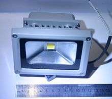
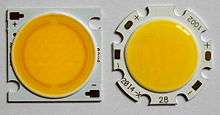
Integrated circuits containing arrays of light-emitting diodes have made LED lighting more efficient. [2]
Chips on board is widely used in electronics and computing, identifiable by "glop tops".
Construction
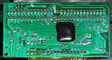
A finished semiconductor wafer is cut into dies. Each die is then physically bonded to the PCB. Three different methods are used to connect the terminal pads of the integrated circuit (or other semiconductor device) with the conductive traces of the printed circuit board.
In "flip chip on board", the device is inverted, with the top layer of metallization facing the circuit board. Small balls of solder are placed on the circuit board traces where connections to the chip are required. The chip and board are passed through a reflow soldering process to make the electrical connections.
In "wire bonding", the chip is attached to the board with an adhesive. Each pad on the device is connected with a fine wire lead that is welded to the pad and to the circuit board. This is similar to the way that an integrated circuit is connected to its lead frame, but instead the chip is wire-bonded directly to the circuit board.
In "tape-automated bonding", thin flat metal tape leads are attached to the device pads, then welded to the printed circuit board.
In all cases, the chip and connections are covered with an encapsulant to reduce entry of moisture or corrosive gases to the chip, and to protect the wire bonds or tape leads from physical damage. [1]
The printed circuit board substrate may be assembled into the final product, for example, as in a pocket calculator, or, in the case of a multi-chip module, the module may be inserted in a socket or otherwise attached to yet another circuit board. The substrate wiring board may include heat-dissipating layers where the mounted devices handle significant power, such as in LED lighting or power semiconductors. Or, the substrate may have low-loss properties required at microwave radio frequencies.
References
- John H. Lau, Chip On Board: Technology for Multichip Modules, Springer Science & Business Media, 1994 ISBN 0442014414 pages 1-3
- Handbook on the Physics and Chemistry of Rare Earths: Including Actinides. Elsevier Science. 1 August 2016. p. 89. ISBN 978-0-444-63705-5.