GeSbTe
GeSbTe (germanium-antimony-tellurium or GST) is a phase-change material from the group of chalcogenide glasses used in rewritable optical discs and phase-change memory applications. Its recrystallization time is 20 nanoseconds, allowing bitrates of up to 35 Mbit/s to be written and direct overwrite capability up to 106 cycles. It is suitable for land-groove recording formats. It is often used in rewritable DVDs. New phase-change memories are possible using n-doped GeSbTe semiconductor. The melting point of the alloy is about 600 °C (900 K) and the crystallization temperature is between 100 and 150 °C.
During writing, the material is erased, initialized into its crystalline state, with low-intensity laser irradiation. The material heats up to its crystallization temperature, but not its melting point, and crystallizes. The information is written at the crystalline phase, by heating spots of it with short (<10 ns), high-intensity laser pulses; the material melts locally and is quickly cooled, remaining in the amorphous phase. As the amorphous phase has lower reflectivity than the crystalline phase, data can be recorded as dark spots on the crystalline background. Recently, novel liquid organogermanium precursors, such as isobutylgermane[1][2][3] (IBGe) and tetrakis(dimethylamino)germane[4][5] (TDMAGe) were developed and used in conjunction with the metalorganics of antimony and tellurium, such as tris-dimethylamino antimony (TDMASb) and di-isopropyl telluride (DIPTe) respectively, to grow GeSbTe and other chalcogenide films of very high purity by metalorganic chemical vapor deposition (MOCVD). Dimethylamino germanium trichloride [6] (DMAGeC) is also reported as the chloride containing and a superior dimethylaminogermanium precursor for Ge deposition by MOCVD.
Material properties

GeSbTe is a ternary compound of germanium, antimony, and tellurium, with composition GeTe-Sb2Te3. In the GeSbTe system, there is a pseudo-line as shown upon which most of the alloys lie. Moving down this pseudo-line, it can be seen that as we go from Sb2Te3 to GeTe, the melting point and glass transition temperature of the materials increase, crystallization speed decreases and data retention increases. Hence, in order to get high data transfer rate, we need to use material with fast crystallization speed such as Sb2Te3. This material is not stable because of its low activation energy. On the other hand, materials with good amorphous stability like GeTe has slow crystallization speed because of its high activation energy. In its stable state, crystalline GeSbTe has two possible configurations: hexagonal and a metastable face-centered cubic (FCC) lattice. When it is rapidly crystallized however, it was found to have a distorted rocksalt structure. GeSbTe has a glass transition temperature of around 100 °C.[7] GeSbTe also has many vacancy defects in the lattice, of 20 to 25% depending on the specific GeSbTe compound. Hence, Te has an extra lone pair of electrons, which are important for many of the characteristics of GeSbTe. Crystal defects are also common in GeSbTe and due to these defects, an Urbach tail in the band structure is formed in these compounds. GeSbTe is generally p type and there are many electronic states in the band gap accounting for acceptor and donor like traps. GeSbTe has two stable states, crystalline and amorphous. The phase change mechanism from high resistance amorphous phase to low resistance crystalline phase in nano-timescale and threshold switching are two of the most important characteristic of GeSbTe.
Applications in phase-change memory
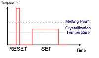
The unique characteristic that makes phase-change memory useful as a memory is the ability to effect a reversible phase change when heated or cooled, switching between stable amorphous and crystalline states. These alloys have high resistance in the amorphous state ‘0’ and are semimetals in the crystalline state ‘1’. In amorphous state, the atoms have short-range atomic order and low free electron density. The alloy also has high resistivity and activation energy. This distinguishes it from the crystalline state having low resistivity and activation energy, long-range atomic order and high free electron density. When used in phase-change memory, use of a short, high amplitude electric pulse such that the material reaches melting point and rapidly quenched changes the material from crystalline phase to amorphous phase is widely termed as RESET current and use of a relatively longer, low amplitude electric pulse such that the material reaches only the crystallization point and given time to crystallize allowing phase change from amorphous to crystalline is known as SET current.
The early devices were slow, power consuming and broke down easily due to the large currents. Therefore, it did not succeed as SRAM and flash memory took over. In the 1980s though, the discovery of germanium-antimony-tellurium (GeSbTe) meant that phase-change memory now needed less time and power to function. This resulted in the success of the rewriteable optical disk and created renewed interest in the phase-change memory. The advances in lithography also meant that previously excessive programming current has now become much smaller as the volume of GeSbTe that changes phase is reduced.
Phase-change memory has many near ideal memory qualities such as non-volatility, fast switching speed, high endurance of more than 1013 read –write cycles, non-destructive read, direct overwriting and long data retention time of more than 10 years. The one advantage that distinguishes it from other next generation non-volatile memory like magnetic random access memory (MRAM) is the unique scaling advantage of having better performance with smaller sizes. The limit to which phase-change memory can be scaled is hence limited by lithography at least until 45 nm. Thus, it offers the biggest potential of achieving ultra-high memory density cells that can be commercialized.
Though phase-change memory offers much promise, there are still certain technical problems that need to be solved before it can reach ultra-high density and commercialized. The most important challenge for phase-change memory is to reduce the programming current to the level that is compatible with the minimum MOS transistor drive current for high-density integration. Currently, the programming current in phase-change memory is substantially high. This high current limits the memory density of the phase-change memory cells as the current supplied by the transistor is not sufficient due to their high current requirement. Hence, the unique scaling advantage of phase-change memory cannot be fully utilized.
The typical phase-change memory device design is shown. It has layers including the top electrode, GST, the GeSbTe layer, BEC, the bottom electrode and the dielectric layers. The programmable volume is the GeSbTe volume that is in contact with the bottom electrode. This is the part that can be scaled down with lithography. The thermal time constant of the device is also important. The thermal time constant must be fast enough for GeSbTe to cool rapidly into the amorphous state during RESET but slow enough to allow crystallization to occur during SET state. The thermal time constant depends on the design and material the cell is built. To read, a low current pulse is applied to the device. A small current ensures the material does not heat up. Information stored is read out by measuring the resistance of the device.
Threshold switching
Threshold switching occurs when GeSbTe goes from a high resistive state to a conductive state at the threshold field of about 56 V/um.[8] This can be seen from the current-voltage (IV) plot, where current is very low in the amorphous state at low voltage until threshold voltage is reached. Current increases rapidly after the voltage snapback. The material is now in the amorphous "ON" state, where the material is still amorphous, but in a pseudo-crystalline electric state. In crystalline state, the IV characteristics is ohmic. There had been debate on whether threshold switching was an electrical or thermal process. There were suggestions that the exponential increase in current at threshold voltage must have been due to generation of carriers that vary exponentially with voltage such as impact ionization or tunneling.[9]
Nano-timescale phase change
Recently, much research has focused on the material analysis of the phase-change material in an attempt to explain the high speed phase change of GeSbTe. Using EXAFS, it was found that the most matching model for crystalline GeSbTe is a distorted rocksalt lattice and for amorphous a tetrahedral structure. The small change in configuration from distorted rocksalt to tetrahedral suggests that nano-timescale phase change is possible[10] as the major covalent bonds are intact and only the weaker bonds are broken.
Using the most possible crystalline and amorphous local structures for GeSbTe, the fact that density of crystalline GeSbTe is less than 10% larger than amorphous GeSbTe, and the fact that free energies of both amorphous and crystalline GeSbTe have to be around the same magnitude, it was hypothesized from density functional theory simulations[11] that the most stable amorphous state was the spinel structure, where Ge occupies tetrahedral positions and Sb and Te occupy octahedral positions, as the ground state energy was the lowest of all the possible configurations. By means of Car-Parrinello molecular dynamics simulations this conjecture have been theoretically confirmed.[12]
Nucleation-domination versus growth-domination
Another similar material is AgInSbTe. It offers higher linear density, but has lower overwrite cycles by 1-2 orders of magnitude. It is used in groove-only recording formats, often in rewritable CDs. AgInSbTe is known as a growth-dominated material while GeSbTe is known as a nucleation-dominated material. In GeSbTe, the nucleation process of crystallization is long with many small crystalline nuclei being formed before a short growth process where the numerous small crystals are joined together. In AgInSbTe, there are only a few nuclei formed in the nucleation stage and these nuclei grow bigger in the longer growth stage such that they eventually form one crystal.[13]
References
- Deo V. Shenai, Ronald L. DiCarlo, Michael B. Power, Artashes Amamchyan, Randall J. Goyette, Egbert Woelk; Dicarlo; Power; Amamchyan; Goyette; Woelk (2007). "Safer alternative liquid germanium precursors for MOVPE". Journal of Crystal Growth. 298: 172–175. Bibcode:2007JCrGr.298..172S. doi:10.1016/j.jcrysgro.2006.10.194.CS1 maint: multiple names: authors list (link)
- Bosi, M.; Attolini, G.; Ferrari, C.; Frigeri, C.; Rimada Herrera, J.C.; Gombia, E.; Pelosi, C.; Peng, R.W. (2008). "MOVPE growth of homoepitaxial germanium". Journal of Crystal Growth. 310 (14): 3282. Bibcode:2008JCrGr.310.3282B. doi:10.1016/j.jcrysgro.2008.04.009.
- Attolini, G.; Bosi, M.; Musayeva, N.; Pelosi, C.; Ferrari, C.; Arumainathan, S.; Timò, G. (2008). "Homo and hetero epitaxy of Germanium using isobutylgermane". Thin Solid Films. 517 (1): 404–406. Bibcode:2008TSF...517..404A. doi:10.1016/j.tsf.2008.08.137.
- M. Longo, O. Salicio, C. Wiemer, R. Fallica, A. Molle, M. Fanciulli, C. Giesen, B. Seitzinger,P.K. Baumann, M. Heuken, S. Rushworth; Salicio; Wiemer; Fallica; Molle; Fanciulli; Giesen; Seitzinger; Baumann; Heuken; Rushworth (2008). "Growth study of GexSbyTez deposited by MOCVD under nitrogen for non‐volatile memory applications". Journal of Crystal Growth. 310 (23): 5053–5057. Bibcode:2008JCrGr.310.5053L. doi:10.1016/j.jcrysgro.2008.07.054.CS1 maint: multiple names: authors list (link)
- A. Abrutis, V. Plausinaitiene, M. Skapas, C. Wiemer, O. Salicio, A. Pirovano, E. Varesi, S. Rushworth, W. Gawelda, J. Siegel; Plausinaitiene; Skapas; Wiemer; Salicio; Pirovano; Varesi; Rushworth; Gawelda; Siegel (2008). "Hot‐Wire Chemical Vapor Deposition of Chalcogenide Materials for Phase Change Memory Applications". Chemistry of Materials. 20 (11): 3557. doi:10.1021/cm8004584. hdl:10261/93002.CS1 maint: multiple names: authors list (link)
- X. Shi; M. Schaekers; F. Leys; R. Loo; M. Caymax; R. Brus; C. Zhao; B. Lamare; E. Woelk; D. Shenai (2006). "Germanium Precursors for Ge and SiGe Deposition". ECS Transactions. 3: 849. doi:10.1149/1.2355880.
- Morales-Sánchez, E.; Prokhorov, E. F.; Mendoza-Galván, A.; González-Hernández, J. (2002-01-15). "Determination of the glass transition and nucleation temperatures in Ge2Sb2Te5 sputtered films". Journal of Applied Physics. AIP Publishing. 91 (2): 697–702. doi:10.1063/1.1427146. ISSN 0021-8979.
- Krebs, Daniel; Raoux, Simone; Rettner, Charles T.; Burr, Geoffrey W.; Salinga, Martin; Wuttig, Matthias (2009). "Threshold field of phase change memory materials measured using phase change bridge devices". Applied Physics Letters. 95 (8): 082101. Bibcode:2009ApPhL..95h2101K. doi:10.1063/1.3210792.
- Pirovano, A.; Lacaita, A.L.; Benvenuti, A.; Pellizzer, F.; Bez, R. (2004). "Electronic Switching in Phase-Change Memories". IEEE Transactions on Electron Devices. Institute of Electrical and Electronics Engineers (IEEE). 51 (3): 452–459. doi:10.1109/ted.2003.823243. ISSN 0018-9383.
- Kolobov, Alexander V.; Fons, Paul; Frenkel, Anatoly I.; Ankudinov, Alexei L.; Tominaga, Junji; Uruga, Tomoya (2004-09-12). "Understanding the phase-change mechanism of rewritable optical media". Nature Materials. Springer Nature. 3 (10): 703–708. doi:10.1038/nmat1215. ISSN 1476-1122.
- Wuttig, Matthias; Lüsebrink, Daniel; Wamwangi, Daniel; Wełnic, Wojciech; Gilleßen, Michael; Dronskowski, Richard (2006-12-17). "The role of vacancies and local distortions in the design of new phase-change materials". Nature Materials. Springer Nature. 6 (2): 122–128. doi:10.1038/nmat1807. ISSN 1476-1122. PMID 17173032.
- Caravati, Sebastiano; Bernasconi, Marco; Kühne, Thomas D.; Krack, Matthias; Parrinello, Michele (2007). "Coexistence of tetrahedral- and octahedral-like sites in amorphous phase change materials". Applied Physics Letters. 91 (17): 171906. arXiv:0708.1302. Bibcode:2007ApPhL..91q1906C. doi:10.1063/1.2801626.
- Coombs, J. H.; Jongenelis, A. P. J. M.; van Es‐Spiekman, W.; Jacobs, B. A. J. (1995-10-15). "Laser‐induced crystallization phenomena in GeTe‐based alloys. I. Characterization of nucleation and growth". Journal of Applied Physics. AIP Publishing. 78 (8): 4906–4917. doi:10.1063/1.359779. ISSN 0021-8979.