Static random-access memory
Static random-access memory (static RAM or SRAM) is a type of random-access memory (RAM) that uses latching circuitry (flip-flop) to store each bit. SRAM is volatile memory; data is lost when power is removed.
| Computer memory types |
|---|
| Volatile |
| RAM |
| Historical |
|
| Non-volatile |
| ROM |
| NVRAM |
| Early stage NVRAM |
| Magnetic |
| Optical |
| In development |
| Historical |
|
The term static differentiates SRAM from DRAM (dynamic random-access memory) which must be periodically refreshed. SRAM is faster and more expensive than DRAM; it is typically used for CPU cache while DRAM is used for a computer's main memory.
History
In 1965,[1] Arnold Farber and Eugene Schlig, working for IBM, created a hard-wired memory cell, using a transistor gate and tunnel diode latch. They replaced the latch with two transistors and two resistors, a configuration that became known as the Farber-Schlig cell. In 1965, Benjamin Agusta and his team at IBM created a 16-bit silicon memory chip based on the Farber-Schlig cell, with 80 transistors, 64 resistors, and 4 diodes.
The first commercial DRAM (built from discrete transistors and capacitors) was produced the same year, 1965.[2]
Applications and uses
Characteristics
Though it can be characterized as volatile memory SRAM exhibits data remanence.[3]
Advantages:
- Simplicity – a refresh circuit is not needed
- Performance
- Reliability
- Low idle power consumption
Disadvantages:
- Price
- Density
- High operational power consumption
Clock rate and power
The power consumption of SRAM varies widely depending on how frequently it is accessed. Several techniques have been proposed to manage power consumption of SRAM-based memory structures.[4]
Contemporary SRAM devices
- general purpose products
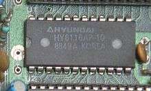
- with asynchronous interface, such as the ubiquitous 28-pin 8K × 8 and 32K × 8 chips (often but not always named something along the lines of 6264 and 62C256 respectively), as well as similar products up to 16 Mbit per chip
- with synchronous interface, usually used for caches and other applications requiring burst transfers, up to 18 Mbit (256K × 72) per chip
- integrated on chip
- as RAM or cache memory in micro-controllers (usually from around 32 bytes up to 128 kilobytes)
- as the primary caches in powerful microprocessors, such as the x86 family, and many others (from 8 KB, up to many megabytes)
- to store the registers and parts of the state-machines used in some microprocessors (see register file)
- on application specific ICs, or ASICs (usually in the order of kilobytes)
- in Field Programmable Gate Array and Complex Programmable Logic Device
Embedded use
Many categories of industrial and scientific subsystems, automotive electronics, and similar, contain static RAM which, in this context, may be referred to as ESRAM.[5] Some amount (kilobytes or less) is also embedded in practically all modern appliances, toys, etc. that implement an electronic user interface. Several megabytes may be used in complex products such as digital cameras, cell phones, synthesizers, game consoles, etc.
SRAM in its dual-ported form is sometimes used for real-time digital signal processing circuits.[6]
In computers
SRAM is also used in personal computers, workstations, routers and peripheral equipment: CPU register files, internal CPU caches and external burst mode SRAM caches, hard disk buffers, router buffers, etc. LCD screens and printers also normally employ static RAM to hold the image displayed (or to be printed). Static RAM was used for the main memory of some early personal computers such as the ZX80, TRS-80 Model 100 and Commodore VIC-20.
Hobbyists
Hobbyists, specifically home-built processor enthusiasts,[7] often prefer SRAM due to the ease of interfacing. It is much easier to work with than DRAM as there are no refresh cycles and the address and data buses are directly accessible. In addition to buses and power connections, SRAM usually requires only three controls: Chip Enable (CE), Write Enable (WE) and Output Enable (OE). In synchronous SRAM, Clock (CLK) is also included.
Types of SRAM
Non-volatile SRAM
Non-volatile SRAM (nvSRAM) has standard SRAM functionality, but they save the data when the power supply is lost, ensuring preservation of critical information. nvSRAMs are used in a wide range of situations – networking, aerospace, and medical, among many others[8] – where the preservation of data is critical and where batteries are impractical.
Pseudo SRAM
Pseudostatic RAM (PSRAM) has a DRAM storage core, combined with a self refresh circuit.[9] They appear externally as a slower SRAM. They have a density/cost advantage over true SRAM, without the access complexity of DRAM.
By transistor type
- Bipolar junction transistor (used in TTL and ECL) – very fast but consumes a lot of power
- MOSFET (used in CMOS) – low power and very common today
By function
- Asynchronous – independent of clock frequency; data in and data out are controlled by address transition.
- Synchronous – all timings are initiated by the clock edge(s). Address, data in and other control signals are associated with the clock signals.
In 1990s, asynchronous SRAM used to be employed for fast access time. Asynchronous SRAM was used as main memory for small cache-less embedded processors used in everything from industrial electronics and measurement systems to hard disks and networking equipment, among many other applications. Nowadays, synchronous SRAM (e.g. DDR SRAM) is rather employed similarly like Synchronous DRAM – DDR SDRAM memory is rather used than asynchronous DRAM. Synchronous memory interface is much faster as access time can be significantly reduced by employing pipeline architecture. Furthermore, as DRAM is much cheaper than SRAM, SRAM is often replaced by DRAM, especially in the case when large volume of data is required. SRAM memory is however much faster for random (not block / burst) access. Therefore, SRAM memory is mainly used for CPU cache, small on-chip memory, FIFOs or other small buffers.
By feature
- Zero bus turnaround (ZBT) – the turnaround is the number of clock cycles it takes to change access to the SRAM from write to read and vice versa. The turnaround for ZBT SRAMs or the latency between read and write cycle is zero.
- syncBurst (syncBurst SRAM or synchronous-burst SRAM) – features synchronous burst write access to the SRAM to increase write operation to the SRAM
- DDR SRAM – Synchronous, single read/write port, double data rate I/O
- Quad Data Rate SRAM – Synchronous, separate read and write ports, quadruple data rate I/O
By flip-flop type
- Binary SRAM
- Ternary SRAM
Design
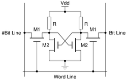
A typical SRAM cell is made up of six MOSFETs. Each bit in an SRAM is stored on four transistors (M1, M2, M3, M4) that form two cross-coupled inverters. This storage cell has two stable states which are used to denote 0 and 1. Two additional access transistors serve to control the access to a storage cell during read and write operations. In addition to such six-transistor (6T) SRAM, other kinds of SRAM chips use 4, 8, 10 (4T, 8T, 10T SRAM), or more transistors per bit.[10][11][12] Four-transistor SRAM is quite common in stand-alone SRAM devices (as opposed to SRAM used for CPU caches), implemented in special processes with an extra layer of polysilicon, allowing for very high-resistance pull-up resistors.[13] The principal drawback of using 4T SRAM is increased static power due to the constant current flow through one of the pull-down transistors.
This is sometimes used to implement more than one (read and/or write) port, which may be useful in certain types of video memory and register files implemented with multi-ported SRAM circuitry.
Generally, the fewer transistors needed per cell, the smaller each cell can be. Since the cost of processing a silicon wafer is relatively fixed, using smaller cells and so packing more bits on one wafer reduces the cost per bit of memory.
Memory cells that use fewer than four transistors are possible – but, such 3T[14][15] or 1T cells are DRAM, not SRAM (even the so-called 1T-SRAM).
Access to the cell is enabled by the word line (WL in figure) which controls the two access transistors M5 and M6 which, in turn, control whether the cell should be connected to the bit lines: BL and BL. They are used to transfer data for both read and write operations. Although it is not strictly necessary to have two bit lines, both the signal and its inverse are typically provided in order to improve noise margins.
During read accesses, the bit lines are actively driven high and low by the inverters in the SRAM cell. This improves SRAM bandwidth compared to DRAMs – in a DRAM, the bit line is connected to storage capacitors and charge sharing causes the bit line to swing upwards or downwards. The symmetric structure of SRAMs also allows for differential signaling, which makes small voltage swings more easily detectable. Another difference with DRAM that contributes to making SRAM faster is that commercial chips accept all address bits at a time. By comparison, commodity DRAMs have the address multiplexed in two halves, i.e. higher bits followed by lower bits, over the same package pins in order to keep their size and cost down.
The size of an SRAM with m address lines and n data lines is 2m words, or 2m × n bits. The most common word size is 8 bits, meaning that a single byte can be read or written to each of 2m different words within the SRAM chip. Several common SRAM chips have 11 address lines (thus a capacity of 2m = 2,048 = 3d words) and an 8-bit word, so they are referred to as "2k × 8 SRAM".
The dimensions of an SRAM cell on an IC is determined by the minimum feature size of the process used to make the IC.
SRAM operation
An SRAM cell has three different states: standby (the circuit is idle), reading (the data has been requested) or writing (updating the contents). SRAM operating in read mode and write modes should have "readability" and "write stability", respectively. The three different states work as follows:
Standby
If the word line is not asserted, the access transistors M5 and M6 disconnect the cell from the bit lines. The two cross-coupled inverters formed by M1 – M4 will continue to reinforce each other as long as they are connected to the supply.
Reading
In theory, reading only requires asserting the word line WL and reading the SRAM cell state by a single access transistor and bit line, e.g. M6, BL. However, bit lines are relatively long and have large parasitic capacitance. To speed up reading, a more complex process is used in practice: The read cycle is started by precharging both bit lines BL and BL, to high (logic 1) voltage. Then asserting the word line WL enables both the access transistors M5 and M6, which causes one bit line BL voltage to slightly drop. Then the BL and BL lines will have a small voltage difference between them. A sense amplifier will sense which line has the higher voltage and thus determine whether there was 1 or 0 stored. The higher the sensitivity of the sense amplifier, the faster the read operation. As the NMOS is more powerful, the pull-down is easier. Therefore, bit lines are traditionally precharged to high voltage. Many researchers are also trying to precharge at a slightly low voltage to reduce the power consumption.[16][17]
Writing
The write cycle begins by applying the value to be written to the bit lines. If we wish to write a 0, we would apply a 0 to the bit lines, i.e. setting BL to 1 and BL to 0. This is similar to applying a reset pulse to an SR-latch, which causes the flip flop to change state. A 1 is written by inverting the values of the bit lines. WL is then asserted and the value that is to be stored is latched in. This works because the bit line input-drivers are designed to be much stronger than the relatively weak transistors in the cell itself so they can easily override the previous state of the cross-coupled inverters. In practice, access NMOS transistors M5 and M6 have to be stronger than either bottom NMOS (M1, M3) or top PMOS (M2, M4) transistors. This is easily obtained as PMOS transistors are much weaker than NMOS when same sized. Consequently, when one transistor pair (e.g. M3 and M4) is only slightly overridden by the write process, the opposite transistors pair (M1 and M2) gate voltage is also changed. This means that the M1 and M2 transistors can be easier overridden, and so on. Thus, cross-coupled inverters magnify the writing process.
Bus behavior
RAM with an access time of 70 ns will output valid data within 70 ns from the time that the address lines are valid. But the data will remain for a hold time as well (5–10 ns). Rise and fall times also influence valid timeslots with approximately 5 ns. By reading the lower part of an address range, bits in sequence (page cycle) one can read with significantly shorter access time (30 ns).[18]
See also
- Flash memory
- Miniature Card, a discontinued SRAM memory card standard
References
- "Nondestructive memory array".
- "Spec Sheet for Toshiba "TOSCAL" BC-1411". www.oldcalculatormuseum.com. Archived from the original on 3 July 2017. Retrieved 8 May 2018.
- Sergei Skorobogatov (June 2002). "Low temperature data remanence in static RAM". University of Cambridge, Computer Laboratory. Retrieved 2008-02-27. Cite journal requires
|journal=(help) - "A Survey of Architectural Techniques For Improving Cache Power Efficiency", S. Mittal, SUSCOM, 4(1), 33–43, 2014
- Fahad Arif (Apr 5, 2014). "Microsoft Says Xbox One's ESRAM is a "Huge Win" – Explains How it Allows Reaching 1080p/60 FPS". Retrieved 2020-03-24.
- Shared Memory Interface with the TMS320C54x DSP (PDF), retrieved 2019-05-04
- "Homemade CPU".
- Computer organization (4th ed.). [S.l.]: McGraw-Hill. 1996-07-01. ISBN 978-0-07-114323-3.
- "3.0V Core Async/Page PSRAM Memory" (PDF). Micron. Retrieved 2019-05-04.
- Kulkarni, Jaydeep P.; Kim, Keejong; Roy, Kaushik (2007). "A 160 mV Robust Schmitt Trigger Based Subthreshold SRAM". IEEE Journal of Solid-State Circuits. 42 (10): 2303. Bibcode:2007IJSSC..42.2303K. doi:10.1109/JSSC.2007.897148.
- United States Patent 6975532: Quasi-static random access memory
- "Area Optimization in 6T and 8T SRAM Cells Considering Vth Variation in Future Processes -- MORITA et al. E90-C (10): 1949 -- IEICE Transactions on Electronics". Archived from the original on 2008-12-05.
- Preston, Ronald P. (2001). "14: Register Files and Caches" (PDF). The Design of High Performance Microprocessor Circuits. IEEE Press. p. 290.
- United States Patent 6975531: 6F2 3-transistor DRAM gain cell
- 3T-iRAM(r) Technology
- SRAM precharge system for reducing write power
- High Speed, Low Power Design Rules for SRAM Precharge and Self-timing under Technology Variations
- "Tentative Toshiba mos digital integrated circuit silicon gate cmos 4,194,304-word by 16-bit cmos pseudo static RAM" (PDF). 070731 toshiba.com