Cadmium arsenide
Cadmium arsenide (Cd3As2) is an inorganic semimetal in the II-V family. It exhibits the Nernst effect.
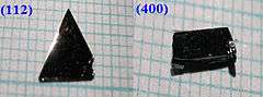 Cd3As2 crystals with (112) and (400) orientations[1] | |
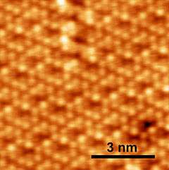 STM image of the (112) surface[1] | |
| Names | |
|---|---|
| Other names
Tricadmium diarsenide | |
| Identifiers | |
3D model (JSmol) |
|
| ChemSpider | |
| ECHA InfoCard | 100.031.336 |
| EC Number |
|
PubChem CID |
|
CompTox Dashboard (EPA) |
|
| |
| |
| Properties | |
| Cd3As2 | |
| Molar mass | 487.08 g/mol |
| Appearance | solid, dark grey |
| Density | 3.031 |
| Melting point | 716 °C (1,321 °F; 989 K) |
| decomposes in water | |
| Structure[1] | |
| Tetragonal, tI160 | |
| I41cd, No. 110 | |
a = 1.26512(3) nm, c = 2.54435(4) nm | |
| Hazards | |
| GHS pictograms |   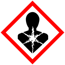  |
| GHS Signal word | Danger |
GHS hazard statements |
H301, H312, H330, H350, H400, H410 |
| P201, P202, P260, P261, P264, P270, P271, P273, P280, P281, P284, P301+310, P302+352, P304+340, P308+313, P310, P311, P312, P320, P321, P322, P330, P363, P391, P403+233 | |
| NFPA 704 (fire diamond) | |
| Lethal dose or concentration (LD, LC): | |
LD50 (median dose) |
no data |
| NIOSH (US health exposure limits): | |
PEL (Permissible) |
[1910.1027] TWA 0.005 mg/m3 (as Cd)[2] |
REL (Recommended) |
Ca[2] |
IDLH (Immediate danger) |
Ca [9 mg/m3 (as Cd)][2] |
Except where otherwise noted, data are given for materials in their standard state (at 25 °C [77 °F], 100 kPa). | |
| Infobox references | |

Properties
Thermal
Cd3As2 dissociates between 220 and 280 °C according to the reaction[3]
- Cd3As2(s) → 3 Cd(g) + 0.5 As4(g)
An energy barrier was found for the nonstoichiometric vaporization of arsenic due to the irregularity of the partial pressures with temperature. The range of the energy gap is from 0.5 to 0.6 eV. Cd3As2 melts at 716 °C and changes phase at 615 °C/[4]
Phase transition
Pure cadmium arsenide undergoes several phase transitions at high temperatures, making phases labeled α (stable), α’, α” (metastable), and β.[5] At 593° the polymorphic transition α → β occurs.
- α-Cd3As2 ↔ α’-Cd3As2 occurs at ~500 K.
- α’-Cd3As2 ↔ α’’-Cd3As2 occurs at ~742 K and is a regular first order phase transition with marked hysteresis loop.
- α”-Cd3As2 ↔ β-Cd3As2 occurs at 868 K.
Single crystal x-ray diffraction was used to determine the lattice parameters of Cd3As2 between 23 and 700 °C. Transition α → α′ occurs slowly and therefore is most likely an intermediate phase. Transition α′ → α″ occurs much faster than α → α′ and has very small thermal hysteresis. This transition results in a change in the fourfold axis of the tetragonal cell, causing crystal twinning. The width of the loop is independent of the rate of heating although it becomes narrower after several temperature cycles.[6]
Electronic
The compound cadmium arsenide has a lower vapor pressure (0.8 atm) than both cadmium and arsenic separately. Cadmium arsenide does not decompose when it is vaporized and re-condensed. Carrier Concentration in Cd3As2 are usually (1–4)×1018 electrons/cm3. Despite having high carrier concentrations, the electron mobilities are also very high (up to 10,000 cm2/(V·s) at room temperature).[7]
In 2014 Cd3As2 was shown to be a semimetal material analogous to graphene that exists in a 3D form that should be much easier to shape into electronic devices.[8][9] Three-dimensional (3D) topological Dirac semimetals (TDSs) are bulk analogues of graphene that also exhibit non-trivial topology in its electronic structure that shares similarities with topological insulators. Moreover, a TDS can potentially be driven into other exotic phases (such as Weyl semimetals, axion insulators and topological superconductors), Angle-resolved photoemission spectroscopy revealed a pair of 3D Dirac fermions in Cd3As2. Compared with other 3D TDSs, for example, β-cristobalite BiO
2 and Na3Bi, Cd3As2 is stable and has much higher Fermi velocities. In situ doping was used to tune its Fermi energy.[9]
Conducting
Cadmium arsenide is a II-V semiconductor showing degenerate n-type semiconductor intrinsic conductivity with a large mobility, low effective mass and highly non parabolic conduction band, or a Narrow-gap semiconductor. It displays an inverted band structure, and the optical energy gap, eg, is less than 0. When deposited by thermal evaporation (deposition), cadmium arsenide displayed the Schottky (thermionic emission) and Poole–Frenkel effect at high electric fields.[10]
Magnetoresistance
Cadmium Arsenide shows very strong quantum oscillations in resistance even at the relatively high temperature of 100K.[11]. This makes it useful for testing cryomagnetic systems as the presence of such a strong signal is a clear indicator of function
Preparation
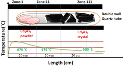
Cadmium arsenide can be prepared as amorphous semiconductive glass. According to Hiscocks and Elliot,[4] the preparation of cadmium arsenide was made from cadmium metal, which had a purity of 6 N from Kock-Light Laboratories Limited. Hoboken supplied β-arsenic with a purity of 99.999%. Stoichiometric proportions of the elements cadmium and arsenic were heated together. Separation was difficult and lengthy due to the ingots sticking to the silica and breaking. Liquid encapsulated Stockbarger growth was created. Crystals are pulled from volatile melts in liquid encapsulation. The melt is covered by a layer of inert liquid, usually B2O3, and an inert gas pressure greater than the equilibrium vapor pressure is applied. This eliminates the evaporation from the melt which allows seeding and pulling to occur through the B2O3 layer.
Crystal structure
The unit cell of Cd3As2 is tetragonal. The arsenic ions are cubic close packed and the cadmium ions are tetrahedrally coordinated. The vacant tetrahedral sites provoked research by von Stackelberg and Paulus (1935), who determined the primary structure. Each arsenic ion was surrounded by cadmium ions at six of the eight corners of a distorted cube and the two vacant sites were at the diagonals.[12]
Nernst effect
Cadmium arsenide is used in infrared detectors using the Nernst effect, and in thin-film dynamic pressure sensors. It can be also used to make magnetoresistors, and in photodetectors.[13]
References
- Sankar, R.; Neupane, M.; Xu, S.-Y.; Butler, C. J.; Zeljkovic, I.; Panneer Muthuselvam, I.; Huang, F.-T.; Guo, S.-T.; Karna, Sunil K.; Chu, M.-W.; Lee, W. L.; Lin, M.-T.; Jayavel, R.; Madhavan, V.; Hasan, M. Z.; Chou, F. C. (2015). "Large single crystal growth, transport property, and spectroscopic characterizations of three-dimensional Dirac semimetal Cd3As2". Scientific Reports. 5: 12966. Bibcode:2015NatSR...512966S. doi:10.1038/srep12966. PMC 4642520. PMID 26272041.
- NIOSH Pocket Guide to Chemical Hazards. "#0087". National Institute for Occupational Safety and Health (NIOSH).
- Westmore, J. B.; Mann, K. H.; Tickner, A. W. (1964). "Mass Spectrometric Study of the Nonstoichiometric Vaporization of Cadmium Arsenide1". The Journal of Physical Chemistry. 68 (3): 606–612. doi:10.1021/j100785a028.
- Hiscocks, S. E. R.; Elliott, C. T. (1969). "On the preparation, growth and properties of Cd3As2". Journal of Materials Science. 4 (9): 784–788. Bibcode:1969JMatS...4..784H. doi:10.1007/BF00551073.
- Pietraszko, A.; Łukaszewicz, K. (1969). "A refinement of the crystal structure of α"-Cd3As2". Acta Crystallographica Section B. 25 (5): 988–990. doi:10.1107/S0567740869003323.
- Pietraszko, A.; Łukaszewicz, K. (1973). "Thermal expansion and phase transitions of Cd3As2 and Zn3As2". Physica Status Solidi A. 18 (2): 723–730. Bibcode:1973PSSAR..18..723P. doi:10.1002/pssa.2210180234.
- Dowgiałło-Plenkiewicz, B.; Plenkiewicz, P. (1979). "Inverted band structure of Cd3As2". Physica Status Solidi B. 94: K57. Bibcode:1979PSSBR..94...57D. doi:10.1002/pssb.2220940153.
- Neupane, M.; Xu, S. Y.; Sankar, R.; Alidoust, N.; Bian, G.; Liu, C.; Belopolski, I.; Chang, T. R.; Jeng, H. T.; Lin, H.; Bansil, A.; Chou, F.; Hasan, M. Z. (2014). "Observation of a three-dimensional topological Dirac semimetal phase in high-mobility Cd3As2". Nature Communications. 5: 3786. arXiv:1309.7892. Bibcode:2014NatCo...5E3786N. doi:10.1038/ncomms4786. PMID 24807399.
- Liu, Z. K.; Jiang, J.; Zhou, B.; Wang, Z. J.; Zhang, Y.; Weng, H. M.; Prabhakaran, D.; Mo, S. K.; Peng, H.; Dudin, P.; Kim, T.; Hoesch, M.; Fang, Z.; Dai, X.; Shen, Z. X.; Feng, D. L.; Hussain, Z.; Chen, Y. L. (2014). "A stable three-dimensional topological Dirac semimetal Cd3As2". Nature Materials. 13 (7): 677–81. Bibcode:2014NatMa..13..677L. doi:10.1038/nmat3990. PMID 24859642.
- Din, M.; Gould, R. D. (2006). "Van der Pauw resistivity measurements on evaporated thin films of cadmium arsenide, Cd3As2". Applied Surface Science. 252 (15): 5508–5511. Bibcode:2006ApSS..252.5508D. doi:10.1016/j.apsusc.2005.12.151.
- Narayanan, A.; Watson, M. D.; Blake, S. F.; Bruyant, N.; Drigo, L.; Chen, Y. L.; Prabhakaran, D.; Yan, B.; Felser, C.; Kong, T.; Canfield, P. C.; Coldea, A. I. (19 March 2015). "Linear Magnetoresistance Caused by Mobility Fluctuations in -Doped". Physical Review Letters. 114 (11). arXiv:1412.4105. doi:10.1103/PhysRevLett.114.117201.
- Ali, M. N.; Gibson, Q.; Jeon, S.; Zhou, B. B.; Yazdani, A.; Cava, R. J. (2014). "The Crystal and Electronic Structures of Cd3As2, the Three-Dimensional Electronic Analogue of Graphene". Inorganic Chemistry. 53 (8): 4062–7. arXiv:1312.7576. doi:10.1021/ic403163d. PMID 24679042.
- Din, M.B.; Gould, R.D. (1998). "High field conduction mechanism of the evaporated cadmium arsenide thin films". ICSE'98. 1998 IEEE International Conference on Semiconductor Electronics. Proceedings (Cat. No.98EX187). p. 168. doi:10.1109/SMELEC.1998.781173. ISBN 0-7803-4971-7.
External links
| Wikimedia Commons has media related to Cadmium arsenide. |