Adhesive bonding
Adhesive bonding (also referred to as gluing or glue bonding) describes a wafer bonding technique with applying an intermediate layer to connect substrates of different types of materials. Those connections produced can be soluble or insoluble.[1] The commercially available adhesive can be organic or inorganic and is deposited on one or both substrate surfaces. Adhesives, especially the well-established SU-8, and benzocyclobutene (BCB), are specialized for MEMS or electronic component production.[2]
The procedure enables bonding temperatures from 1000 °C down to room temperature.[1] The most important process parameters for achieving a high bonding strength are:[3]
- adhesive material
- coating thickness
- bonding temperature
- processing time
- chamber pressure
- tool pressure
Adhesive bonding has the advantage of relatively low bonding temperature as well as the absence of electric voltage and current. Based on the fact that the wafers are not in direct contact, this procedure enables the use of different substrates, e.g. silicon, glass, metals and other semiconductor materials. A drawback is that small structures become wider during patterning which hampers the production of an accurate intermediate layer with tight dimension control.[3] Further, the possibility of corrosion due to out-gassed products, thermal instability and penetration of moisture limits the reliability of the bonding process.[4] Another disadvantage is the missing possibility of hermetically sealed encapsulation due to higher permeability of gas and water molecules while using organic adhesives.[5]
Overview
The adhesive bonding with organic materials, i.e. BCB or SU-8, has simple process properties and the ability to form high aspect ratio micro structures. The bonding procedure is based on polymerization reaction of organic molecules to form long polymer chains during annealing. This cross-link reaction forms BCB and SU-8 to a solid polymer layer.[3]
The intermediate layer is applied by spin-on, spray-on, screen-printing, embossing, dispensing or block printing on one or two substrate surfaces. The adhesive layer thickness depends on the viscosity, rotational speed and the applied tool pressure. The procedural steps of adhesive bonding are divided into the following:[1]
- Cleaning and pre-treatment of substrates surfaces
- Application of adhesive, solvent or other intermediate layers
- Contacting substrates
- Hardening intermediate layer
The most established adhesives are polymers that enable connections of different materials at temperatures ≤ 200 °C.[5] Due to these low process temperature metal electrodes, electronics and various micro-structures can be integrated on the wafer. The structuring of polymers as well as the realization of cavities over movable elements are possible using photo-lithography or dry etching.[5]
The hardening conditions depend on the used materials. Hardening of the adhesives are possible:[1]
- at room temperature
- through heating cycles
- using UV light
- by applying pressure
Surface preparation of plastics
To create a desirable surface for the adhesive bonding of plastics, there are three major requirements: the weak boundary layer of the given material must be removed or chemically modified to create a strong boundary layer; the surface energy of the adherend should be higher than that of the adhesive for good wetting; and the surface profile can be improved to provide mechanical interlocking. Meeting one of these major requirements will improve bonding; however, the most desirable surface will incorporate all three requirements. Numerous techniques are available to help produce a desirable surface for adhesive bonding.[6]
Degreasing
When preparing a surface for adhesive bonding, all oil and grease contamination must be removed in order to form a strong bond. Although the surface may appear to be clean, it is important to still use the degreasing process.[7] Prior to performing the degreasing process, the compatibility of the solvent used and the adherend must be considered to prevent irreversible damage of the surface or part.[7]
Vapor degreasing
One method of degreasing is that of vapor degreasing, in which the adherend is dipped in a solvent. When removed from the solvent, the vapors condense on the surface of the adherend and dissolve any contaminants that had existed. These contaminants then drip off the adherend with the condensed vapors.[8]
In lieu of vapor degreasing
The other method of degreasing requires a cloth or rag soaked in solvent, which can be used to wipe down the surface of the adherend to remove contaminants.[8] It is important that all residue that had been left behind from the solvents be removed, so that there is no detrimental effects to the adhesive bonding.[7]
Following degreasing process
After degreasing, a good test to determine cleanliness of the surface is to use a drop of water. If the drop spreads on the surface, a low contact angle and good wettability has been achieved, which indicates the surface is clean and ready for application of the adhesive. If the drop beads up or retains its shape, the degreasing process should be repeated.[7]
Abrasion

In general, abrasion is superior to other methods of surface preparations due to the fact that it is simple to perform, and it does not produce a significant amount of waste.[8] To prepare the adherend for bonding, the surface can be sanded or grit blasted with an abrasive material to roughen the surface and remove any loose material.[9][8] Rough surfaces produce stronger bonds because they have an increased surface area for the adhesive to bond to as compared to a relatively smooth surface.[7] In addition, roughening the surface will also increase mechanical interlocking.[6] Following abrasion, the adherend should always be wiped with solvent or an aqueous detergent solution to clean the surface of any oils and loose material and then dried. After this process is complete, the adhesive can be applied.[9]
Peel ply
For a peel ply, a thin, woven piece of material is applied to the adherend during fabrication.[9] Because the material is woven, it will leave a torturous surface when removed, which will improve bonding by mechanical interlocking.[6] Prior to adhesive bonding, the woven material acts to protect the surface of the adherend from contaminates. When an adhesive is ready to be applied, the material can be peeled off, leaving a rough and clean surface for bonding.[9]
Corona discharge treatment
Corona discharge treatment (CDT) is typically used to improve adhesion of ink or coatings on plastic films.[6] In the CDT, an electrode is connected to a high voltage source. The film travels on a roller that is covered with a dielectric layer and is grounded. When a voltage is applied, the electrical discharge causes ionization of air, and a plasma is formed.[10] In doing so, the surface of the film is oxidized, thus improving wetting and adhesion.[6] Additionally, the discharge reacts with molecules of the adherend to form free radicals, which react with oxygen and eventually form polar groups that increase the surface energy of the adherend.[7] Another way CDT improves bonding is that it roughens the adherend by removing the amorphous regions of the surface, which increases the surface area and improves adhesive bonding.[7] Depending on the type of adherend being treated with CDT, the treatment times may differ. Some adherends may require longer treating times to achieve the same surface energy.[7]
Flame treatment
In flame treatment, a mixture of gas and air is used to produce a flame that is ran over the surface of the adherend.[8] The flame that is produced must be oxidizing in order to produce an effective treatment. This means that the flame is blue in color.[7] Flame treatment can be performed by using a setup similar to the CDT in which plastic film travels across a roller while the flame contacts it. In addition to more sophisticated methods, flame treatment can also be done by hand with the use of a torch. However, even and steady treatment of the surface is more difficult to obtain. [6] Once the flame treatment is completed, the part can be gently cleaned with water and air dried, which will ensure that an excess of oxides are not formed.[8] Control during the flame treatment is critical. Too much of the treatment will degrade the plastic, which will lead to poor adhesion. Too little of a treatment will not modify the surface enough and will also lead to poor adhesion.[7] An additional aspect of flame treatment that must be considered is possible deformation to the adherend. Precise control of the flame will prevent this from occurring.[8]
Plasma treatment
Plasma is a gas excited by electrical energy, and contains approximately an equal density of positive- and negative-charged ions.[8][6] The interaction of the electrons and ions in the plasma with the surface oxidizes the surface and forms free radicals.[6] The oxidation of the surface removes unwanted contaminants and improves adhesion.[8] In addition to removing contaminates, the plasma treatment also introduces polar groups that increase the surface energy of the adherend.[7] Plasma treatment can produce adhesive bonds up to four times stronger than compared to chemically or mechanically treated adherends.[7] In general, plasma treatment is not used often in industry because it is required to be performed below atmospheric pressure. This creates an expensive and less cost effective process.[6]
Chemical treatment
Chemical treatments are used to change the composition and structure of the surface of the adherend and are often used in addition to degreasing and abrasion to maximize the strength of the adhesive bond.[8] In addition to this, they increase the chance of other bonding forces to occur, such as hydrogen, dipole, and van der Waals bonding between the adherend and the adhesive.[8] Chemical solutions can be applied to the surface of an adherend to either clean or alter the surface of the adherend, depending on the chemical used. Solvents are used to simply clean the surfaces of any contaminates or debris. They do not increase the surface energy of the adherend.[6] To modify the surface of the adherend, acid solutions can be used to etch and oxidize the surface. These solutions must be carefully prepared in order to ensure good bonding strength is developed.[8] These treatments can be made more effective by increasing the time and temperature of the application. However, too long of time can lead to excess reaction products that form and can hinder the bonding performance between the adhesive and adherend.[7] As with other surface preparation methods, a good test to assure a good chemical treatment is to put a drop of water on the surface of the adherend. If the drop flattens or spreads out, it means the surface of the adherend has good wettability and should allow for good bonding.[8] A final consideration when using chemical treatments is that of safety. The chemicals used in the treatments can be hazardous to human health and before using any, the material safety data sheet for the particular chemical should be referenced.[8]
Ultraviolet radiation treatment
Ultraviolet (UV) radiation plays a role in numerous surface treatments, including some of the fore mentioned treatments, although it may not be the dominating factor. An example of a UV treatment where UV radiation is the primary factor that effects the surface preparation is with the use of excimer lasers. Excimer lasers are extremely high energy and use to create pulses of radiation. When the laser makes contact with the surface of the adherend, it removes a layer of material, therefore cleaning the surface. In addition, if the UV radiation laser treatment is performed in the presence of air, the surface of the adherend can be oxidized, thus improving the surface energy. Finally, the radiation pulses can be used to create specific surface patterns that will increase surface area and improve bonding.[6]
SU-8
Overview
SU-8 is a 3 component UV-sensitive negative photo-resist based on epoxy resin, gamma butyrolactone and triaryl sulfonium salt. The SU-8 polymerizes at approximately 100 °C and is temperature-stable up to 150 °C. This polymer adhesive is CMOS and bio-compatible and has excellent electrical, mechanical and fluidic properties. It also has a high cross-linking density, high chemical resistance and high thermal stability. The viscosity depends on the mixture with the solvent for different layer thicknesses (1.5 to 500 µm). Using multilayer coating a layer thickness up to 1 mm is reachable. The lithographic structuring is based on a photoinitiator triaylium-sulfonium that releases lewis acid during UV radiation. This acid works as catalyst for the polymerization. The connection of the molecules is activated over different annealing steps, so called post exposure bake (peb).[5] Using SU-8 can achieve a high bonding yield. In addition, the substrate flatness, clean room conditions and the wettability of the surface are important factors to achieve good bond results.[11]
Procedural steps
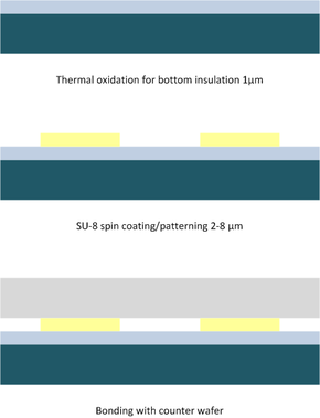
The standard process (compare to figure "Schematic bonding process") consists of applying SU-8 on the top wafer by spin-on or spray-on of thin layers (3 to 100 µm).
Subsequently, the structuring of the photo-resist using direct UV light exposure is applied but can also be achieved through deep reactive-ion-etching (DRIE). During coating and structuring of the SU-8 the tempering steps before and after exposure have to be considered. Based on thermal layer stress the risk of crack formation exists. While coating the photoresist the formation of voids due to the layer thickness inhomogeneity has to be avoided. The adhesive layer thickness should be larger than the flatness imperfection of the wafer to establish good contact.[3] The procedural steps based on a typical example are:
- Cleaning Top wafer
- Thermal oxidation
- Dehydration
- Spin coating the SU-8
- Softbake
- 120 s at 65 °C
- 300 s to 95 °C
- Cooling down
- Exposure with 165 to 200 mJ⁄cm3
- Post-exposure-bake
- 2 to 120 min at 50 to 120 °C
- to room temperature
- relaxation time
- development
- rinsing and dry spinning
- hard bake at 50 to 150 °C for 5 to 120 min
For non-planar wafer surfaces or free standing structures, spin-coating is not a very successful SU-8 deposition method. As a result, spray-on is mainly used on structured wafers.[11] The bonding takes place at the polymerization temperature of SU-8 at approximately 100 °C.
The soft-bake allows that high residual solvent content minimizes intrinsic stress and improves cross-linking. The SU-8 layer is patterned using soft contact exposure followed by post-exposure bake. The non-exposed SU-8 is removed by immersing in, e.g. propylene glycol methyl ether acetate (PGMEA).[12]
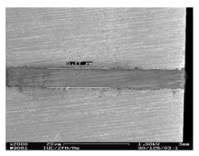
Ensuring void-free bonding a homogeneous layer thickness of the SU-8 over the wafer surface is important (compare to cross section photo).[5]
To ensure good contact of the wafer pair a constant pressure between 2.5 and 4.5 bar during bonding is applied.[3]
The frames should be kept above the non-flatness value of the wafer, based on the fact that defects usually are caused by the curvature of the wafer.[3] A shear strength of the bonded wafer pair of about 18 to 25 MPa is achievable.[11]
Examples
Adhesive bonding using SU-8 is applicable to zero-level packaging technology for low cost MEMS packaging. Metallic feed-throughs can be used for electrically connections to packed elements through the adhesive layer.[12] Also biomedical and micro fluidic devices are fabricated based on SU-8 adhesive layer as well as micro fluidic channels, movable micro-mechanical components, optical waveguides and UV-LIGA components.[13]
Benzocyclobutene (BCB)
Overview
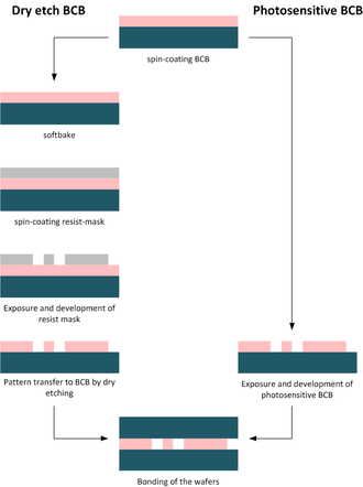
Benzocyclobutene (BCB) is a hydrocarbon that is widely used in electronics.[15] BCB exists in a dry etch and a photosensitive version, each requiring different procedural steps for structuring (compare BCB process flow).[16]
It does release only small amounts of by-products during curing which enables a void-free bond. This polymer ensures very strong bonds and excellent chemical resistance to numerous acids, alkalines and solvents. The BCB is over 90% transparent to visible light that enables the use for optical MEMS applications.[15]
Compared to other polymers the BCB has a low dielectric constant and dielectric loss.[17] The polymerization of BCB is taking place at a temperature around 250 to 300 °C and it is stable up to 350 °C. Using BCB does not ensure a sufficient hermeticity of sealed cavities for MEMS.[18]
Procedural steps
The procedural steps for dry etch BCB are:
- Cleaning
- Supplying the adhesion promoter
- Drying of the primer
- BCB deposition
- Photosensitive BCB
- Exposure and development
- Dry etch BCB
- Pre-bake/soft-cure
- Patterning of the BCB layer by lithography and dry-etching
- Bonding at specific temperature, ambient pressure for specific amount of time
- Post-bake/hard-cure to form solid BCB monomer layer
The wafers can be cleaned using H2O2 + H2SO4 or oxygen plasma. The cleaned wafers are rinsed with DI water and dried at elevated temperature, e.g. 100 to 200 °C for 120 min.[16]
The adhesion promoter with a specific thickness is deposited, i.e. spin-coated or contact printed on the wafer to improve the bonding strength. Spray coating is preferable when the adhesive is deposited on free standing structures.[18]

Subsequently, the BCB layer is spin or spray coated, usually 1 to 50 µm thick, to the same wafer. To prevent that the patterned layer has a lower bond strength than the unpatterned layer, due to the cross-linking of the polymer, a soft-curing step is applied before bonding.[19] The pre-curing of the BCB takes place for several minutes on the hot plate at a specific temperature ≤ 300 °C. The soft cure prevents bubble formation and unbonded areas[20] as well as the distortion of the adhesive layer during compression to improve the alignment accuracy.[21] The degree of polymerization should not be over 50%, so it is robust enough to be patterned and still sufficiently adhesive to be bonded.[19]
If the BCB is hard-baked (far over 50%), it loses its adhesives properties and results in an increased amount of void formation. But also if the soft-curing is above 210 °C the adhesive cures too much, so that the material is not soft and sticky enough to achieve a high bonding strength.[14]
The substrates with the intermediate layer are pressed together with subsequent curing results in a bond.[4] The post-bake process is applied at 180 to 320 °C for 30 to 240 min usually in a specific atmosphere or vacuum in the bond chamber. This is necessary to hard-cure the BCB. The vacuum prevents air trapped in the bond interface and pumps out the gases of the out-gassing residual solvents during annealing. The temperature and the curing time are variable, so with a higher temperature curing time can be reduced based on a quicker cross-linking.[15] The final bonding layer thickness depends on the thickness of the cured BCB, the spinning speed and the shrink rate.[14]
Examples
Adhesive bonding using a BCB intermediate layer is a possible method for packaging and sealing of MEMS devices, also structured Si wafers. Its use is specified for applications that does not require hermetic sealing, i.e. MOEMS mirror arrays, RF MEMS switches and tunable capacitors. BCB bonding is used in the fabrication of channels for fluidic devices, for transfer protruding surface structures as well as for CMOS controller wafers and integrated SMA microactuators.
Technical Specifications
| Materials |
Substrate:
Intermediate layer:
|
| Temperature |
|
| Advantages |
|
| Drawbacks |
|
| Researches |
|
References
- Wiemer, M.; Frömel, J.; Gessner, T. (2003). "Trends der Technologieentwicklung im Bereich Waferbonden". In W. Dötzel (ed.). 6. Chemnitzer Fachtagung Mikromechanik & Mikroelektronik. 6. pp. 178–188.
- Gessner, T.; Otto, T.; Wiemer, M.; Frömel, J. (2005). "Wafer bonding in micro mechanics and microelectronics - an overview". The World of Electronic Packaging and System Integration. pp. 307–313.
- Wiemer, M.; Jia, C.; Töpper, M.; Hauck, K. (2006). "Wafer Bonding with BCB and SU-8 for MEMS Packaging". Electronics Systemintegration Technology Conference. 1st Electronics Systemintegration Technology Conference, 2006. 1. pp. 1401–1405. doi:10.1109/ESTC.2006.280194. ISBN 1-4244-0552-1.
- Wolffenbuttel, R. F. (1997). "Low-temperature intermediate Au-Si wafer bonding; eutectic or silicide bond". Sensors and Actuators A: Physical. 62 (1–3). pp. 680–686. doi:10.1016/S0924-4247(97)01550-1.
- Reuter, D.; Frömel, J.; Schwenzer, G.; Bertz, A.; Gessner, T. (October 2003). "Selektives Niedertemperaturbonden mit SU-8 für Wafer-Level-Verkappung von mikromechanischen Strukturen". In W. Dötzel (ed.). 6. Chemnitzer Fachtagung Mikromechanik & Mikroelektronik. 6. Technische Universität Chemnitz. pp. 90–94.
- Pocius, Alphonsus (2012). Adhesion and Adhesives Technology. Cincinnati: Hanser Publications. ISBN 978-1-56990-511-1.
- Ebnesajjad, Sina; Ebnesajjad, Cyrus F. (2014). Surface treatment of materials for adhesion bonding (2nd ed.). Kidlington, Oxford: William Andrew. ISBN 9780323264358. OCLC 871691428.
- Ebnesajjad, Sina (2011). Handbook of adhesives and surface preparation : technology, applications and manufacturing. Amsterdam: William Andrew/Elsevier. ISBN 9781437744613. OCLC 755779919.
- Wegman, Raymond F.; Van Twisk, James (2013). Surface preparation techniques for adhesive bonding (2nd ed.). William Andrew. ISBN 9781455731268. OCLC 819636705.
- Chan CM. (1999) Surface treatment of polypropylene by corona discharge and flame. In: Karger-Kocsis J. (eds) Polypropylene. Polymer Science and Technology Series, vol 2. Springer, Dordrecht
- Yu, L.; Tay, F. E. H.; Xu, G.; Chen, B.; Avram, M.; Iliescu, C. (2006). "Adhesive bonding with SU-8 at wafer level for microfluidic devices". Journal of Physics: Conference Series. 34 (1). p. 776.
- Murillo, G.; Davis, Z. J.; Keller, S.; Abadal, G.; Agusti, J.; Cagliani, A.; Noeth, N.; Boisen, A.; Barniol, N. (2010). "Novel SU-8 based vacuum wafer-level packaging for MEMS devices". Microelectronic Engineering. 87 (5–8). pp. 1173–1176. doi:10.1016/j.mee.2009.12.048.
- Patel, J. N.; Kaminska, B.; Gray, B. L.; Gates, B. D. (2008). "PDMS as a sacrificial substrate for SU-8-based biomedical and microfluidic applications". Journal of Micromechanics and Microengineering. 18 (9). p. 095028.
- Oberhammer, J.; Niklaus, F.; Stemme, G. (2003). "Selective wafer-level adhesive bonding with benzocyclobutene for fabrication of cavities". Sensors and Actuators A: Physical. 105 (3). pp. 297–304. doi:10.1016/S0924-4247(03)00202-4.
- Niklaus, F.; Andersson, H.; Enoksson, P.; Stemme, G. (2001). "Low temperature full wafer adhesive bonding of structured wafers". Sensors and Actuators A: Physical. 92 (1–3). pp. 235–241. doi:10.1016/S0924-4247(01)00568-4.
- Christiaens, I.; Roelkens, G.; De Mesel, K.; van Thourhout, D.; Baets, R. (2005). "Thin-film devices fabricated with benzocyclobutene adhesive wafer bonding". Journal of Lightwave Technology. 23 (2). pp. 517–523. doi:10.1109/JLT.2004.841783.
- Töpper, M.; Lopper, C.; Zoschke, K.; Scherpinski, K.; Fritzsch, T.; Dietrich, L.; Lutz, M.; Ehrmann, O.; Reichl, H. BCB - A Thin Film Polymer for Advanced Wafer Level Packaging and MEMS Applications (Report). Fraunhofer IZM and TU Berlin. pp. 292–298.
- Oberhammer, J.; Niklaus, F.; Stemme, G. (2004). "Sealing of adhesive bonded devices on wafer level". Sensors and Actuators A: Physical. 110 (1–3). pp. 407–412. doi:10.1016/j.sna.2003.06.003.
- Oberhammer, J.; Stemme, G. (2004). "Contact printing for improved bond-strength of patterned adhesive full-wafer bonded 0-level packages". 17th IEEE International Conference on Micro Electro Mechanical Systems (MEMS). pp. 713–716. doi:10.1109/MEMS.2004.1290684.
- Niklaus, F.; Enoksson, P.; Kalvesten, E.; Stemme, G. (2000). "Void-free full wafer adhesive bonding". The 13th Annual International Conference on Micro Electro Mechanical Systems (MEMS). pp. 247–252. doi:10.1109/MEMSYS.2000.838524.
- Farrens, S. (2008). "Wafer-Bonding Technologies and Strategies for 3D ICs". In Tan, C. S.; Gutmann, R. J.; Reif, L. R. (eds.). Wafer Level 3-D ICs Process Technology. Integrated Circuits and Systems. Springer US. pp. 49–85. doi:10.1007/978-0-387-76534-1.