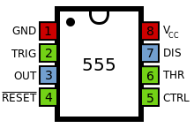
555 timer IC
The 555 timer IC is an integrated circuit (chip) used in a variety of timer, delay, pulse generation, and oscillator applications. Derivatives provide two (556) or four (558) timing circuits in one package.[2] Introduced in 1972[3] by Signetics,[4] the 555 is still in widespread use due to its low price, ease of use, and stability. Numerous companies have made the original bipolar timers and similar low-power CMOS timers too. As of 2003, it was estimated that 1 billion units were manufactured every year.[5] The 555 is the most popular integrated circuit ever manufactured.[6][7]
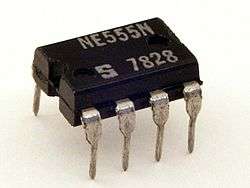 Signetics NE555 in 8-pin DIP package | |
| Type | Active, Integrated circuit |
|---|---|
| Invented | Hans Camenzind (1971) |
| First production | 1972 |
| Electronic symbol | |
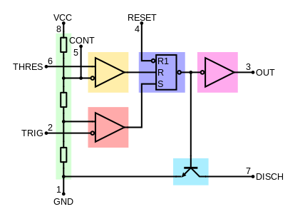 Internal block diagram[1] | |
History
The timer IC was designed in 1971 by Hans Camenzind under contract to Signetics.[3] In 1968, he was hired by Signetics to develop a phase-locked loop (PLL) IC. He designed an oscillator for PLLs such that the frequency did not depend on the power supply voltage or temperature. Signetics subsequently laid off half of its employees due to the 1970 recession, and development on the PLL was thus frozen.[8] Camenzind proposed the development of a universal circuit based on the oscillator for PLLs and asked that he develop it alone, borrowing equipment from Signetics instead of having his pay cut in half. Other engineers argued the product could be built from existing parts; however, the marketing manager approved the idea.
The first design for the 555 was reviewed in the summer of 1971. Assessed to be without error, it proceeded to layout design. A few days later, Camenzind got the idea of using a direct resistance instead of a constant current source finding later that it worked. The change decreased the required 9 pins to 8 so the IC could be fit in an 8-pin package instead of a 14-pin package. This revised design passed a second design review with the prototypes completed in October 1971 as the NE555V (plastic DIP) and SE555T (metal TO-5).[5] The 9-pin copy had been already released by another company founded by an engineer who attended the first review and retired from Signetics; that firm withdrew its version soon after the 555 was released.[8] The 555 timer was manufactured by 12 companies in 1972 and it became a best selling product.[8]
Later, Hans Camenzind designed the ZSCT1555 timer for Zetex Semiconductors, which is no longer manufactured.
Part name
It has been falsely hypothesized that the 555 got its name from the three 5 kΩ resistors within the bipolar IC.[9] Hans Camenzind has stated that the part number was arbitrary, thus it was simply a coincidence they matched.[5][8] The "NE" and "SE" prefix letters of the original Signetic parts numbers, NE555 and SE555, were temperature designations for analog chips, where "NE" was commercial temperature family and "SE" was military temperature family.
Design
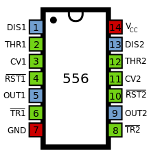
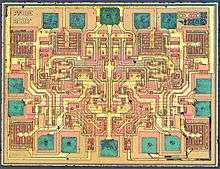
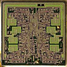
Depending on the manufacturer, the standard 555 package includes 25 transistors, 2 diodes and 15 resistors on a silicon chip installed in an 8-pin dual in-line package (DIP-8).[10] Variants available include the 556 (a DIP-14 combining two complete 555s on one chip),[11] and 558 / 559 (both a DIP-16 combining four reduced-functionality timers on one chip).[2]
The NE555 parts were commercial temperature range, 0 °C to +70 °C, and the SE555 part number designated the military temperature range, −55 °C to +125 °C. These were available in both high-reliability metal can (T package) and inexpensive epoxy plastic (V package) packages. Thus the full part numbers were NE555V, NE555T, SE555V, and SE555T.
Low-power CMOS versions of the 555 are also available, such as the Intersil ICM7555 and Texas Instruments LMC555, TLC555, TLC551.[12][13] [14][15] CMOS timers use significantly less power than bipolar timers; CMOS timers also cause less supply noise than bipolar version when the output switches states.
Internal schematic
The internal block diagram and schematic of the 555 timer are highlighted with the same color across all three drawings to clarify how the chip is implemented:[2]
- Green: Between the positive supply voltage VCC and the ground GND is a voltage divider consisting of three identical resistors, which create two reference voltages at 1⁄3 VCC and 2⁄3 VCC. The latter is connected to the "Control Voltage" pin. All three resistors have the same resistance, 5 kΩ for bipolar timers, 100 kΩ (or higher) for CMOS timers. It is a false myth that the 555 IC got its name from these three 5 kΩ resistors.[5]
- Yellow: The comparator negative input is connected to the higher-reference voltage divider of 2⁄3 VCC (and "Control" pin), and comparator positive input is connected to the "Threshold" pin.
- Red: The comparator positive input is connected to the lower reference voltage divider of 1⁄3 VCC, and comparator negative input is connected to the "Trigger" pin.
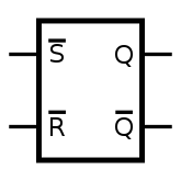
- Purple: An SR flip-flop stores the state of the timer and is controlled by the two comparators. The "Reset" pin overrides the other two inputs, thus the flip-flop (and therefore the entire timer) can be reset at any time.
- Pink: The output of the flip-flop is followed by an output stage with push-pull (P.P.) output drivers that can load the "Output" pin with up to 200 mA for bipolar timers, lower for CMOS timers.
- Cyan: Also, the output of the flip-flop turns on a transistor that connects the "Discharge" pin to the ground.
- 555 internal block diagram[1]
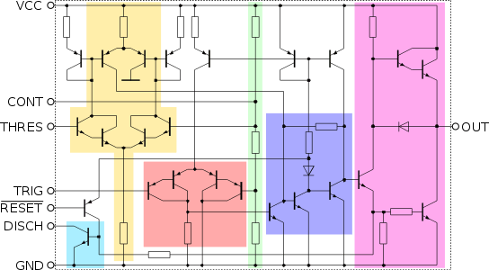 555 internal schematic of bipolar version
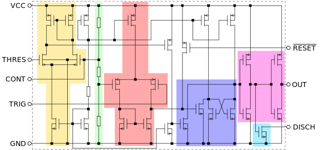 555 internal schematic of CMOS version
Pinout
The pinout of the 8-pin 555 timer[1] and 14-pin 556 dual timer[16] are shown in the following table. The 556 is conceptually two 555 timers that share power pins, thus each half is split across two columns.[2]
| 555 pin# | 556:1st pin# | 556:2nd pin# | Pin name | Pin direction | Pin description[1][16][2] |
|---|---|---|---|---|---|
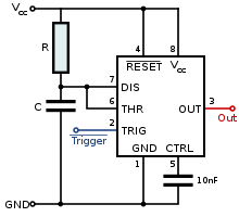
| 1 | 7 | 7 | GND | Power |
Ground supply: this pin is the ground reference voltage (zero volts). For bipolar timers, one or more decoupling capacitor(s) (between this pin and VCC) are required because of current surges during output switching.[17] |
| 2 | 6 | 8 | TRIG | Input |
Trigger: when the voltage at this pin falls below 1⁄2 of CONT pin voltage (1⁄3 VCC except when CONT is driven by an external signal), the OUT pin goes high and a timing interval starts. As long as this pin continues to be kept at a low voltage, the OUT pin will remain high. |
| 3 | 5 | 9 | OUT | Output |
Output: this pin is a push-pull (P.P.) output that is driven to either a low state (GND pin) or a high state (for bipolar timers, VCC pin minus approximately 1.7 Volts) (for CMOS timers, VCC pin). For bipolar timers, this pin can drive up to 200mA, but CMOS timers are able to drive less (varies by chip). For bipolar timers, if this pin drives an edge-sensitive input of a digital logic chip, a 100 to 1000 pF decoupling capacitor (between this pin and GND) may need to be added to prevent double triggering,[2] though a higher bypass capacitor on VCC power pin can help alleviate this problem.[17] |
| 4 | 4 | 10 | RESET | Input |
Reset: a timing interval may be reset by driving this pin to GND, but the timing does not begin again until this pin rises above approximately 0.7 Volts. This pin overrides the trigger, which in turn overrides the threshold. If this pin is not used, it should be connected to VCC to prevent electrical noise causing a reset. |
| 5 | 3 | 11 | CONT (CV) | Input |
Control (or Control Voltage): this pin provides access to the internal voltage divider (2⁄3 VCC by default). By applying a voltage to this pin, the timing characteristics can be changed. In astable mode, this pin can be used to frequency-modulate the output. If this pin is not used, it should be connected to a 10 nF decoupling capacitor (between this pin and GND) to ensure electrical noise doesn't affect the internal voltage divider.[2] |
| 6 | 2 | 12 | THRES | Input |
Threshold: when the voltage at this pin is greater than the voltage at CONT pin (2⁄3 VCC except when CONT is driven by an external signal), then the "OUT high" timing interval ends, causing the output to go low. |
| 7 | 1 | 13 | DISCH | Output |
Discharge: For bipolar times, this pin is an open-collector (O.C.) output, CMOS timers are open-drain O.D. This pin can be used to discharge a capacitor between intervals, in phase with output. In bistable mode and schmitt trigger mode, this pin is unused, which allows it to be used as an alternate output. |
| 8 | 14 | 14 | VCC | Power |
Positive supply: For bipolar timers, the voltage range is typically 4.5 to 16 Volts, some are spec'ed for up to 18 Volts, though most will operate as low as 3 Volts. For CMOS timers, the voltage range is typically 2 to 15 Volts, some are spec'ed for up to 18 Volts, and some are spec'ed as low as 1 Volt. See the supply min and max columns in the derivatives table in this article. For bipolar timers, one or more decoupling capacitor(s) (between this pin and GND) are required because of current surges during output switching.[2][17] |
Modes
The 555 IC has the following operating modes:
- Astable (free-running) mode – the 555 can operate as an electronic oscillator. Uses include LED and lamp flashers, pulse generation, logic clocks, tone generation, security alarms, pulse position modulation and so on. The 555 can be used as a simple ADC, converting an analog value to a pulse length (e.g., selecting a thermistor as timing resistor allows the use of the 555 in a temperature sensor and the period of the output pulse is determined by the temperature). The use of a microprocessor-based circuit can then convert the pulse period to temperature, linearize it and even provide calibration means.
- Monostable (one-shot) mode – in this mode, the 555 functions as a "one-shot" pulse generator. Applications include timers, missing pulse detection, bounce-free switches, touch switches, frequency divider, capacitance measurement, pulse-width modulation (PWM), and so on.
- Bistable (flip-flop) mode – the 555 operates as a SR flip-flop. Uses include bounce-free latched switches.
- Schmitt Trigger (inverter) mode - the 555 operates as a Schmitt trigger inverter gate which converts a noisy input into a clean digital output.
Astable
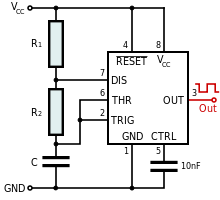
| Frequency | C | R1 | R2 | Duty cycle |
|---|---|---|---|---|
| 0.1 Hz (+0.048%) | 100uF | 8.2K | 68K | 52.8% |
| 1 Hz (+0.048%) | 10uF | 8.2K | 68K | 52.8% |
| 10 Hz (+0.048%) | 1uF | 8.2K | 68K | 52.8% |
| 100 Hz (+0.048%) | 100nF | 8.2K | 68K | 52.8% |
| 1 kHz (+0.048%) | 10nF | 8.2K | 68K | 52.8% |
| 10 kHz (+0.048%) | 1nF | 8.2K | 68K | 52.8% |
| 100 kHz (+0.048%) | 100pF | 8.2K | 68K | 52.8% |
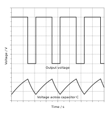
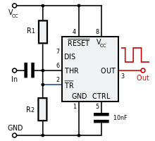
In the astable configuration, the 555 timer puts out a continuous stream of rectangular pulses having a specific frequency. The astable configuration is implemented using two resistors, and , and one capacitor . In this configuration, the control pin is not used, thus it is connected to ground through a 10 nF decoupling capacitor to shunt electrical noise. The threshold and trigger pins are connected to the capacitor , thus they have the same voltage. Initially, the capacitor is not charged, thus the trigger pin receives zero voltage which is less than a third of the supply voltage. Consequently, the trigger pin causes the output to go high and the internal discharge transistor to go to cut-off mode. Since the discharge pin is no longer short-circuited to ground, the current flows through the two resistors, and , to the capacitor charging it. The capacitor starts charging until the voltage becomes two-thirds of the supply voltage. At this instance, the threshold pin causes the output to go low and the internal discharge transistor to go into saturation mode. Consequently, the capacitor starts discharging through till it becomes less than a third of the supply voltage, in which case, the trigger pin causes the output to go high and the internal discharge transistor to go to cut-off mode once again. And the cycle repeats.


In the first pulse, the capacitor charges from zero to two-thirds of the supply voltage, however, in later pulses, it only charges from one-third to two-thirds of the supply voltage. Consequently, the first pulse has a longer high time interval compared to later pulses. Moreover, the capacitor charges through both resistors but only discharges through , thus the high interval is longer than the low interval. This is shown in the following equations.
The high time interval of each pulse is given by:

The low time interval of each pulse is given by:

Hence, the frequency of the pulse is given by:


and the duty cycle (%) is given by:

where is in seconds (time), is in ohms (resistance), is in farads (capacitance), is the natural log of 2 constant, which is 0.693147181 (rounded to 9 trailing digits) but commonly is rounded to fewer digits in 555 timer books and datasheets as 0.7 or 0.69 or 0.693.


Resistor requirements:
- power capability of must be greater than , per Ohm's law.


- Particularly with bipolar 555s, low values of must be avoided so that the output stays saturated near zero volts during discharge, as assumed by the above equation. Otherwise, the output low time will be greater than calculated above.
The first cycle will take appreciably longer than the calculated time, as the capacitor must charge from 0V to 2⁄3 of VCC from power-up, but only from 1⁄3 of VCC to 2⁄3 of VCC on subsequent cycles.
To have an output high time shorter than the low time (i.e., a duty cycle less than 50%) a fast diode (i.e. 1N4148 signal diode) can be placed in parallel with R2, with the cathode on the capacitor side. This bypasses R2 during the high part of the cycle so that the high interval depends only on R1 and C, with an adjustment based the voltage drop across the diode. The voltage drop across the diode slows charging on the capacitor so that the high time is longer than the expected and often-cited ln(2)*R1C = 0.693 R1C. The low time will be the same as above, 0.693 R2C. With the bypass diode, the high time is

where Vdiode is when the diode's "on" current is 1⁄2 of Vcc/R1 which can be determined from its datasheet or by testing. As an extreme example, when Vcc= 5 and Vdiode= 0.7, high time = 1.00 R1C which is 45% longer than the "expected" 0.693 R1C. At the other extreme, when Vcc= 15 and Vdiode= 0.3, the high time = 0.725 R1C which is closer to the expected 0.693 R1C. The equation reduces to the expected 0.693 R1C if Vdiode= 0.
The operation of RESET in this mode is not well-defined. Some manufacturers' parts will hold the output state to what it was when RESET is taken low, others will send the output either high or low.
Monostable
.png)
| Time | C | R |
|---|---|---|
| 100 uS (-0.026%) | 1nF | 91K |
| 1 mS (-0.026%) | 10nF | 91K |
| 10 mS (-0.026%) | 100nF | 91K |
| 100 mS (-0.026%) | 1uF | 91K |
| 1 S (-0.026%) | 10uF | 91K |
| 10 S (-0.026%) | 100uF | 91K |
In monostable mode, the output pulse ends when the voltage on the capacitor equals 2⁄3 of the supply voltage. The output pulse width can be lengthened or shortened to the need of the specific application by adjusting the values of R and C.[19]
Assume initially the output of the monostable is zero, the output of flip-flop(Q bar) is 1 so that the discharging transistor is on and the voltage across a capacitor is zero. One of the inputs of the upper comparator is at 2/3 of supply voltage and the other is connected to the capacitor. For a lower comparator, one of the inputs is trigger pulse and the other is connected at 1/3 of the supply voltage. Now the capacitor charges towards supply voltage(Vcc). When the trigger input is applied at the trigger pin the output of the lower comparator is 0 and the upper comparator is 0. The output of flip-flop remains unchanged therefore the output is 0. when the voltage across the capacitor crosses the 1/3 of the Vcc the output of lower comparator changes from 0 to 1. Therefore, the output of monostable is one and the discharging transistor is still off and the voltage across capacitor charges towards Vcc from 1/3 of Vcc,
When the voltage across the capacitor crosses 2/3 of VCC, the output of the upper comparator changes from 0 to 1, therefore the output of monostable is 0 and the discharging transistor is on and the capacitor discharges through this transistor as it offers low resistance path. The cycle repeats continuously. The charging and discharging of the capacitor depends on the time constant RC.
The voltage across capacitor is given by vc = Vcc(1-e^(-t/RC)) at t=T. Since vc =(2/3)Vcc, therefore 2/3Vcc = Vcc(1-e^(-T/RC)), thus reduced to T = RC ln(3) seconds.
The output pulse width of time t, which is the time it takes to charge C to 2⁄3 of the supply voltage, is given by

where is in seconds (time), is in ohms (resistance), is in farads (capacitance), is the natural log of 3 constant, which is 1.098612289 (rounded to 9 trailing digits) but commonly is rounded to fewer digits in 555 timer books and datasheets as 1.1 or 1.099.

While using the timer IC in monostable mode, the main disadvantage is that the time span between any two triggering pulses must be greater than the RC time constant.[20] Conversely, ignoring closely spaced pulses is done by setting the RC time constant to be larger than the span between spurious triggers. (Example: ignoring switch contact bouncing.)
Bistable
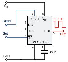
In bistable mode, the 555 timer acts as an SR flip-flop. The trigger and reset inputs (pins 2 and 4 respectively on a 555) are held high via pull-up resistors while the threshold input (pin 6) is grounded. Thus configured, pulling the trigger momentarily to ground acts as a 'set' and transitions the output pin (pin 3) to VCC (high state). Pulling the reset input to ground acts as a 'reset' and transitions the output pin to ground (low state). No timing capacitors are required in a bistable configuration. Pin 7 (discharge) is left unconnected, or may be used as an open-collector output.[21]
Schmitt trigger

A 555 timer can be used to create a Schmitt trigger inverter gate which converts a noisy input into a clean digital output. The input signal should be connected through a series capacitor which then connects to the trigger and threshold pins. A resistor divider, from VCC to GND, is connected to the previous tied pins. The reset pin is tied to VCC.
Packages

In 1972, Signetics originally released the 555 timer in DIP-8 and TO5-8 metal can packages, and the 556 timer was released in DIP-14 package.[4]
In 2020, the 555 was available in through-hole packages as DIP-8 (2.54mm pitch),[22] and surface-mount packages as SO-8 (1.27mm pitch), SSOP-8 / TSSOP-8 / VSSOP-8 (0.65mm pitch), BGA (0.5mm pitch).[1]
In 2020, the dual 556 timer was available in through-hole packages as DIP-14 (2.54mm pitch),[16] and surface-mount packages as SO-14 (1.27mm pitch) and SSOP-14 (0.65mm pitch).
The MIC1555 is a CMOS 555-type timer with 3 fewer pins available in SOT23-5 (0.95mm pitch) surface-mount package.[23]
Specifications
These specifications apply to bipolar NE555. Other 555 timers can have different specifications depending on the grade (industrial, military, medical, etc.). These values should be considered "ballpark" values; the current official datasheet from the exact manufacturer of each chip should be consulted instead for parameter limitation recommendations.
| Part number | NE555 |
| IC Process | Bipolar |
| Supply voltage (VCC) | 4.5 to 16 V |
| Supply current (VCC = +5 V) | 3 to 6 mA |
| Supply current (VCC = +15 V) | 10 to 15 mA |
| Output current (maximum) | 200 mA |
| Maximum Power dissipation | 600 mW |
| Power consumption (minimum operating) | 30 mW @ 5V, 225 mW @ 15V |
| Operating temperature | 0 to 70 °C |
Derivatives
Numerous companies have manufactured one or more variants of the 555, 556, 558 timers over the past decades as many different part numbers. The following is a partial list:
| Manufacturer | Part Number | Production Status | IC Process | Timer Total | Supply Min (Volt) | Supply Max (Volt) | 5V Supply Iq (μA) | Frequency Max (MHz) | Remarks | Datasheet |
|---|---|---|---|---|---|---|---|---|---|---|
| Custom Silicon Solutions (CSS) | CSS555 | Yes | CMOS | 1 | 1.2 | 5.5 | 4.3 | 1.0 | Lowest current, internal EEPROM, requires programmer | [24][25][26] |
| Diodes Inc | ZSCT1555 | No | Bipolar | 1 | 0.9 | 6 | 150 | 0.33 | Lowest voltage, designed by Camenzind | [27] |
| Japan Radio Company (JRC) | NJM555 | No | Bipolar | 1 | 4.5 | 16 | 3000 | 0.1* | Also available in SIP-8 | [22] |
| Microchip | MIC1555 | Yes | CMOS | 1* | 2.7 | 18 | 240 | 5.0* | Reduced features, only available in SOT23-5 | [23] |
| ON | MC1455 | Yes | Bipolar | 1 | 4.5 | 16 | 3000 | 0.1* | — | [28] |
| Renesas | ICM7555 | Yes | CMOS | 1 | 2 | 18 | 40 | 1.0 | Lowest current of common parts | [12] |
| Renesas | ICM7556 | Yes | CMOS | 2 | 2 | 18 | 80 | 1.0 | Lowest current of common parts | [12] |
| Signetics | NE555 | No | Bipolar | 1 | 4.5 | 16 | 3000 | 0.1* | First 555 timer, DIP-8 or TO5-8 | [4][11][29][2] |
| Signetics | NE556 | No | Bipolar | 2 | 4.5 | 16 | 6000 | 0.1* | First 556 timer, DIP-14 | [11][2] |
| Signetics | NE558 | No | Bipolar | 4* | 4.5 | 16 | 4800* | 0.1* | First 558 timer, DIP-16 | [2] |
| STMicroelectronics (ST) | TS555 | Yes | CMOS | 1 | 2 | 16 | 110 | 2.7 | — | [30] |
| Texas Instruments (TI) | LM555 | Yes | Bipolar | 1 | 4.5 | 16 | 3000 | 0.1* | Slightly different than NE555[31] | [20] |
| Texas Instruments | LM556 | No | Bipolar | 2 | 4.5 | 16 | 6000 | 0.1* | Slightly different than NE556[31] | [32] |
| Texas Instruments | LMC555 | Yes | CMOS | 1 | 1.5 | 15 | 100 | 3.0 | Also available in DSBGA-8 | [13] |
| Texas Instruments | NE555 | Yes | Bipolar | 1 | 4.5 | 16 | 3000 | 0.1* | — | [1] |
| Texas Instruments | NE556 | Yes | Bipolar | 2 | 4.5 | 16 | 6000 | 0.1* | — | [16] |
| Texas Instruments | TLC551 | Yes | CMOS | 1 | 1 | 15 | 170 | 1.8 | Lowest voltage of common parts | [15] |
| Texas Instruments | TLC552 | Yes | CMOS | 2 | 1 | 15 | 340 | 1.8 | Lowest voltage of common parts | [33] |
| Texas Instruments | TLC555 | Yes | CMOS | 1 | 2 | 15 | 170 | 2.1 | — | [14] |
| Texas Instruments | TLC556 | Yes | CMOS | 2 | 2 | 15 | 340 | 2.1 | — | [34] |
| X-REL | XTR655 | Yes | SOI | 1 | 2.8 | 5.5 | 170 | 4.0 | Extreme (-60°C to +230°C), ceramic DIP-8 or bare die | [35] |
- Table notes
- All information in the above table was pulled from references in the datasheet column, except where denoted below.
- For the "Timer Total" column, a "*" denotes parts that are missing 555 timer features.
- For "Iq" column, a 5 volt supply was chosen as a common voltage to make it easier to compare. The value for Signetics NE558 is an estimate because NE558 datasheets don't state Iq at 5V.[2] The value listed in this table was estimated by comparing the 5V to 15V ratio of other bipolar datasheets, then derating the 15V parameter for the NE558 part, which is denoted by the "*".
- For the "Frequency Max" column, a "*" denotes values that may not be the actual maximum frequency limit of the part. The MIC1555 datasheet discusses limitations from 1 to 5 MHz.[23] Though most bipolar timers don't state the maximum frequency in their datasheets, they all have a maximum frequency limitation of hundreds of kHz across their full temperature range. Section 8.1 of the Texas Instruments NE555 datasheet[1] states a value of 100 kHz, and their website shows a value of 100 kHz in timer comparison tables, which is overly conservative. In Signetics App Note 170, states that most devices will oscillate up to 1 MHz, however when considering temperature stability it should be limited to about 500 kHz.[2] The application note from HFO mentions that at higher supply voltages the maximum power dissipation of the circuit might limit the operating frequency, as the supply current increases with frequency.[36]
- For the "Manufacturer" column, the following associates historical 555 timer manufacturers to current company names.
- Fairchild Semiconductor was sold to ON Semiconductor in 2016.[37] ON Semiconductor was founded in 1999 as a spinoff of Motorola Semiconductor Components Group.[38] The MC1455 started as a Motorola product.
- Intersil was sold to Renesas Electronics in 2017.[39] The ICM7555 and ICM7556 started as Intersil products.
- Micrel was sold to Microchip Technology in 2015.[40] The MIC1555 started as a Micrel product.
- National Semiconductor was sold to Texas Instruments in 2011.[41] The LM555 and LM556 started as a National Semiconductor products.
- Signetics was sold to Philips Semiconductor in 1975, later to NXP Semiconductors in 2006.[42]
- Zetex Semiconductors was sold to Diodes Incorporated in 2008.[43] The ZSCT1555 started as a Zetex product.
556 dual timer
The dual version is called 556. It features two complete 555 timers in a 14 pin package, only the two power supply pins are shared between the two timers.[16][11] In 2020, the bipolar version was available as the NE556,[16], and the CMOS versions were available as the Intersil ICM7556 and Texas Instruments TLC556 and TLC552, see derivatives table in this article.[12][34][33]
558 quad timer
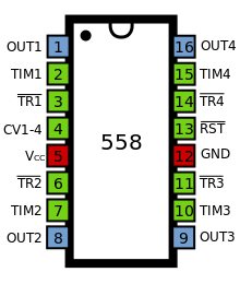
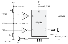
The quad version is called 558. It has four reduced-functionality timers in a 16 pin package (four complete 555 timer circuits would have required 26 pins).[2] Since the timers in the 558 is uniquely different than the 555 and 556, the 558 was not as popular. Currently, the 558 is not manufactured by any major chip companies (possibly not by any companies), thus the 558 should be treated as obsolete. Parts are still available from a limited number of sellers as "new old stock" (N.O.S.).[44]
Partial list of differences between 558 and 555 chips:[2]
- One VCC and one GND, similar to 556 chip.
- Four "Reset" are tied together internally to one external pin (558).
- Four "Control Voltage" are tied together internally to one external pin (558).
- Four "Triggers" are falling-edge sensitive (558), instead of level sensitive (555).
- Two resistors in the voltage divider (558), instead of three resistors (555).
- One comparator (558), instead of two comparators (555).
- Four "Output" are open-collector (O.C.) type (558), instead of push-pull (P.P.) type (555). Since the 558 outputs are open-collector, pull-up resistors are required to "pull up" the output to the positive voltage rail when the output is in a high state. This means the high state only sources a small amount of current through the pull-up resistor.
Example applications
Stepped tone generator
This circuit requires two 555 or one 556 to generate a variety of sounds.
Joystick and game paddles
The Apple II microcomputer used a quad timer 558 in monostable (or "one-shot") mode to interface up to four "game paddles" or two joysticks to the host computer.[46] It also used a single 555 for flashing the display cursor.[47]
The original IBM PC used a similar circuit for the game port on the "Game Control Adapter" 8-bit ISA card (IBM part number 1501300).[45][48] In this joystick interface circuit, the capacitor of the RC network (see Monostable Mode above) was generally a 10 nF capacitor to ground with a series 2.2 KΩ resistor to the game port connector.[45] The external joystick was plugged into the adapter card. Internally it had two potentiometers (100 to 150 KΩ each), one for X and other for Y direction. The center wiper pin of the potentiometer was connected to an Axis wire in the cord and one end of the potentiometer was connected to the 5 Volt wire in the cord. The joystick potentiometer acted as a variable resistor in the RC network.[48] By moving the joystick, the resistance of the joystick increased from a small value up to about 100 kΩ.[48][48]
Software running in the IBM PC computer started the process of determining the joystick position by writing to a special address (ISA bus I/O address 201h).[45][48][49] This would result in a trigger signal to the quad timer, which would cause the capacitor of the RC network to begin charging and cause the quad timer to output a pulse. The width of the pulse was determined by how long it took the capacitor to charge up to 2⁄3 of 5 V (or about 3.33 V), which was in turn determined by the joystick position.[48][49] The software then measured the pulse width to determine the joystick position. A wide pulse represented the full-right joystick position, for example, while a narrow pulse represented the full-left joystick position.[48]
See also
- RC circuit
- Counter (digital)
- Operational amplifier
- List of LM-series integrated circuits
- List of linear integrated circuits
- 4000-series integrated circuits, List of 4000-series integrated circuits
- 7400-series integrated circuits, List of 7400-series integrated circuits
- Push–pull output, Open-collector/drain output, Three-state output
References
- "NE555 Datasheet" (PDF). Texas Instruments. September 2014. Archived (PDF) from the original on June 28, 2017.
- "Linear LSI Data and Applications Manual" (PDF). Signetics. 1985. Archived from the original on April 5, 2016.
(see 555/556/558 datasheets and AN170/AN171 appnotes)
- Fuller, Brian (15 August 2012). "Hans Camenzind, 555 timer inventor, dies". EE Times. Retrieved 27 December 2016.
- "Linear Vol1 Databook". Signetics. 1972. Archived from the original on January 9, 2013.
- Ward, Jack (2004). The 555 Timer IC – An Interview with Hans Camenzind. The Semiconductor Museum. Retrieved 2010-04-05
- Tony R. Kuphaldt. "Lessons In Electric Circuits: Volume VI - Experiments". Chapter 8.
- Albert Lozano. "Introduction to Electronic Integrated Circuits (Chips)"
- Carmenzind, Hans (2010). Translated by 三宅, 和司. "タイマIC 555 誕生秘話" [The birth of the 555 timer IC]. トランジスタ技術 (Transistor Technology) (in Japanese). CQ出版. 47 (12): 73, 74. ISSN 0040-9413.
- Scherz, Paul (2000) "Practical Electronics for Inventors", p. 589. McGraw-Hill/TAB Electronics. ISBN 978-0-07-058078-7. Retrieved 2010-04-05.
- van Roon, Fig 3 & related text.
- "555/556 Timers Databook". Signetics. 1973. Archived from the original on October 4, 2012.
- "ICM7555-556 Datasheet" (PDF). Intersil. June 2016. Archived from the original (PDF) on June 29, 2017.
- "LMC555 Datasheet" (PDF). Texas Instruments. July 2016. Archived (PDF) from the original on June 28, 2017.
- "TLC555 Datasheet" (PDF). Texas Instruments. August 2016. Archived (PDF) from the original on June 28, 2017.
- "TLC551 Datasheet" (PDF). Texas Instruments. September 1997. Archived (PDF) from the original on June 29, 2017.
- "NE556 Datasheet" (PDF). Texas Instruments. June 2006. Archived (PDF) from the original on June 29, 2017.
- Decoupling capacitors and the 555 timer IC; May 17, 2014.
- van Roon Chapter: "Astable operation".
- van Roon, Chapter "Monostable Mode". (Using the 555 timers as a logic clock)
- "LM555 Datasheet" (PDF). Texas Instruments. January 2015. Archived (PDF) from the original on June 29, 2017.
- 555 Timer Operating Modes; 555-timer-circuits.com
- "NJM555 Datasheet" (PDF). Japan Radio Company. November 2012. Archived from the original (PDF) on June 29, 2017.
- "MIC1555 Datasheet" (PDF). Microchip Technology. March 2017.
- "CSS555 Datasheet" (PDF). Custom Silicon Solutions. July 2012. Archived (PDF) from the original on June 29, 2017.
- "CSS555 Part Search". Jameco Electronics.
- "The Remarkable CSS555". Nuts & Volts Magazine. February 2016. Archived from the original on May 27, 2020.
- "ZSCT1555 Datasheet" (PDF). Diodes Incorporated. July 2006. Archived (PDF) from the original on June 29, 2017.
- "MC1455 Datasheet" (PDF). ON Semiconductor. December 2009. Archived (PDF) from the original on May 22, 2020.
- "Analog Applications Manual". Signetics. 1979. Archived from the original on January 9, 2013.
(see chapter 6)
- "TS555 Datasheet" (PDF). STMicroelectronics. June 2015. Archived (PDF) from the original on May 26, 2020.
- "How the NE555 and LM555 are Different". TubeTime. April 2, 2016. Archived from the original on June 6, 2020.
- "LM556 Datasheet" (PDF). Texas Instruments. October 2015. Archived from the original (PDF) on June 29, 2017.
- "TLC552 Datasheet" (PDF). Texas Instruments. May 1988. Archived (PDF) from the original on June 29, 2017.
- "TLC556 Datasheet" (PDF). Texas Instruments. September 1997. Archived (PDF) from the original on June 29, 2017.
- "XTR655 Datasheet" (PDF). X-REL Semiconductor. September 2013. Archived (PDF) from the original on June 29, 2017.
- Reick, Ullrich (1986-03-01). Zeitgeber-IS B 555 / B 556 (PDF) (in German). Halbleiterwerk Frankfurt (Oder).
- "ON Semiconductor Successfully Completes Acquisition of Fairchild Semiconductor". Business Wire. September 19, 2016. Archived from the original on September 19, 2016.
- "Former Motorola group emerges as ON Semiconductor". EE Times. August 5, 1999. Archived from the original on June 7, 2020.
- "Renesas and Intersil Announce Final Regulatory Approval for Renesas' Acquisition of Intersil". Renesas Electronics. February 22, 2017. Archived from the original on June 13, 2020.
- "Microchip Technology Completes Micrel Acquisition". Power Electronics. August 12, 2015. Archived from the original on May 22, 2020.
- "Texas Instruments completes acquisition of National Semiconductor". Texas Instruments. September 23, 2011. Archived from the original on May 22, 2020.
- "NXP Semiconductors history". Silicon Valley Historical Association. 2008. Archived from the original on March 21, 2020.
- "Diodes Incorporated closes acquisition of Zetex". LEDs Magazine. June 13, 2008. Archived from the original on May 22, 2020.
- NE558 Stock Search; Octopart.
- Game Control Adapter Manual and Schematic (PDF). IBM. Retrieved June 30, 2017.
- "Joysticks, Paddles, Buttons, and Game Port Extenders for Apple II, Atari 400/800, Commodore VIC-20". Creative Computing Video & Arcade Games. 1 (1): 106. Spring 1983. Retrieved June 30, 2017.
- Apple II Reference Manual and Schematics (PDF). Apple Inc. January 1978. Retrieved June 30, 2017.
- "PC Analog Joystick Interface". epanorama.net. Retrieved June 30, 2017.
- Eggebrecht, Lewis C. (1983). Interfacing to the IBM Personal Computer (1st ed.). Sams Publishing. pp. 197–199. ISBN 978-0-672-22027-2.
Further reading
- Books
- 555 Timer Applications Sourcebook Experiments; 2nd Ed; Howard Berlin; BPB Publications; 218 pages; 2008; ISBN 978-8176567909. (1st Ed in 1978)
- Timer/Generator Circuits Manual; 1st Ed; R.M. Marston; Newnes; 276 pages; 1990; ISBN 978-0434912919.
- Engineer's Mini-Notebook – 555 Timer IC Circuits; 3rd Ed; Forrest Mims III; Radio Shack; 33 pages; 1989; ASIN B000MN54A6. (1st Ed in 1984)
- IC Timer Cookbook; 2nd Ed; Walt Jung; Sams Publishing; 384 pages; 1983; ISBN 978-0672219320. (1st Ed in 1977)
- 110 IC Timer Projects; Jules Gilder; Hayden; 115 pages; 1979; ISBN 978-0810456884.
- IC 555 Projects; E.A. Parr; Bernard Babani Publishing; 144 pages; 1978; ISBN 978-0859340472.
- Books with timer chapters
- Lessons in Electric Circuits - Volume VI - Experiments; Tony Kuphaldt; Open Book Project; 423 pages; 2010. (Chapter 6 and 8)
- Designing Analog Chips; Hans Camenzind (inventor of 555 timer); Virtual Bookworm; 244 pages; 2005; ISBN 978-1589397187. (Chapter 11)
- Timer, Op Amp, and Optoelectronic Circuits and Projects; Forrest Mims III; Master Publishing; 128 pages; 2004; ISBN 978-0945053293. (Chapter 1)
- Linear LSI Data and Applications Manual; Signetics; 1250 pages; 1985. (Appnotes AN170/171 and Datasheets NE555/6/8)
- Analog Applications Manual; Signetics; 418 pages; 1979. (Chapter 6)
- TTL Cookbook; Don Lancaster; Sams Publishing; 412 pages; 1974; ISBN 978-0672210358. (Chapter 4)
- Datasheets
- See links in "Derivatives" table and "References" section in this article.
External links
| Wikimedia Commons has media related to 555 timer IC. |
- Common Mistakes When Using a 555 Timer
- Using the 555 Timer IC in Special or Unusual Circuits - Nuts & Volts magazine
- 555 tear down - a look inside the chip - Ken Shirriff
- 555 timer online calculators: astable multivibrator, monostable multivibrator
| Authority control |
|
|---|