Open collector
An open collector is a common type of output found on many integrated circuits (IC), which behaves like a switch that is either connected to ground or disconnected. Instead of outputting a signal of a specific voltage or current, the output signal is applied to the base of an internal NPN transistor whose collector is externalized (open) on a pin of the IC. The emitter of the transistor is connected internally to the ground pin. If the output device is a MOSFET the output is called open drain and it functions in a similar way. For example, the I²C bus is based on this concept.
Function
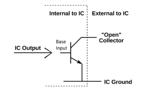
In the picture, the transistor base is labeled "IC output". This is a signal from the internal IC logic to the transistor. This signal controls the transistor switching. The external output is the transistor collector; the transistor forms an interface between the internal IC logic and parts external to the IC.
On schematic component symbols, the open output is indicated with these symbols:[1]
- ⎐ for a pin that outputs low-Z L or hi-Z H (or ⎒ with an internal pull-up resistor)
- ⎏ for a pin that outputs hi-Z L or low-Z H (or ⎑ with an internal pull-down resistor)
The output forms either an open circuit or a connection to ground. The output usually consists of an external pull-up resistor, which raises the output voltage when the transistor is turned off. When the transistor connected to this resistor is turned on, the output is forced to nearly 0 volts. Open-collector outputs can be useful for analog weighting, summing, limiting, etc., but such applications are not discussed here.
A three-state logic device is unlike an open collector device, because it comprises transistors to source and sink current in both logic states, as well as a control to turn off both transistors and isolate the output.
Applications of open-collector devices
Because the pull-up resistor is external and does not need to be connected to the chip supply voltage, a lower or higher voltage than the chip supply voltage can be used instead (providing it does not exceed the absolute maximum rating of the chip's output). Open collector circuits are therefore sometimes used to interface different families of devices that have different operating voltage levels. The open-collector transistor can be rated to withstand a higher voltage than the chip supply voltage. This technique is commonly used by logic circuits operating at 5 V or lower to drive devices such as motors, 12 V relays, 50 V vacuum fluorescent displays, or Nixie tubes requiring more than 100 V.
Another advantage is that more than one open-collector output can be connected to a single line. If all outputs attached to the line are in the high-impedance state, the pull-up resistor will hold the wire in a high voltage (logic 1) state. If one or more device outputs are in the logic 0 (ground) state, they will sink current and pull the line voltage toward ground. This wired logic connection has several uses. Open-collector devices are commonly used to connect multiple devices to one interrupt request signal or a shared bus such as I²C. This enables one device to drive the bus without interference from the other inactive devices. If open-collector devices were not used, then the outputs of the inactive devices would attempt to hold the bus voltage high, resulting in unpredictable output.

By tying the output of several open collectors together, the common line becomes a "wired AND" (positive-true logic) or "wired OR" (negative-true logic) gate. A "wired AND" behaves like the boolean AND of the two (or more) gates in that it will be logic 1 whenever (all) are in the high impedance state, and 0 otherwise. A "wired OR" behaves like the Boolean OR for negative-true logic, where the output is LOW if any of its inputs are low.
SCSI-1 devices use open collector for electrical signaling.[2] SCSI-2 and SCSI-3 may use EIA-485.
One problem with open-collector devices is power consumption, since the pullup resistor dissipates power whenever the output is pulled low, and the higher the desired operating speed, the lower the resistor value (i.e. the stronger the pullup) needs to be, resulting in increased consumption. Even in the 'off' state, they often have a few nanoamperes of leakage current (the exact amount varies with temperature).
MOSFET
The analogous connection used with MOS transistors is an open-drain connection. Open-drain outputs can be useful for analog weighting, summing, and limiting as well as digital logic. An open drain terminal is connected to ground when a high voltage (logic 1) is applied to the gate, yet presents a high impedance when a low voltage (logic 0) is applied to the gate. This high impedance state occurs because the terminal is at an undefined voltage (floating) thus such a device requires an external pull-up resistor connected to the positive voltage rail (logic 1) in order to provide a logic 1 as output.
Microelectronic devices using open drain signals (such as microcontrollers) may provide a weak (high-resistance) internal pull-up resistor to connect the terminal in question to the positive power supply of the device. Such weak pullups, often on the order of 100 kΩ, reduce power usage by keeping input signals from floating and may avoid the need for an external pull-up component. External pullups are stronger (lower resistance, perhaps 3 kΩ) to reduce signal rise times (like with I²C) or to minimize noise (like on system RESET inputs). Internal pullups can usually be disabled if they are not wanted.
POD Pseudo open drain
The pseudo open drain (POD) drivers have a strong pull-down strength but a weaker pullup strength. A pure open-drain driver, by comparison, has no pullup strength except for leakage current: all the pull-up action is on the external termination resistor. This is why the term "pseudo" has to be used here: there is some pull-up on the driver side when output is at high state, the remaining pull-up strength is provided by parallel-terminating the receiver at the far end to the HIGH voltage, often using a switchable, on-die terminator instead of a separate resistor. The purpose of all this is to reduce the overall power demand compared to using both strong pullup and strong pull-down, as in drivers such as HSTL.[3] DDR4 memory uses POD12 drivers but with the same driver strength (34 Ω/48 Ω) for pull-down (RonPd) and pull-up (RonPu). The term POD in DDR4 referring only for termination type that is only parallel pull-up without the pull-down termination at the far end. The reference point (VREF) for the input is not half-supply as was in DDR3 and may be higher.

JEDEC standardized the POD15,[4] the POD125,[5] the POD135[6] and the POD12[7] for 1.5V, 1.35V and 1.2V interface supply voltages. A comparison[8] of both DDR3 and DDR4 termination schemes in terms of skew, eye aperture and power consumption was published in late 2011.
See also
References
- "Overview of IEEE Standard 91-1984 Explanation of Logic Symbols" (PDF). Texas Instruments. Texas Instruments. 1996. Retrieved February 12, 2020.
- "Overview of SCSI Standards & Cables". Archived from the original on 2008-12-10. 081214 scsita.org
- Addenddum No. 6 to JESD8 - High Speed Transceiver Logic (HSTL)- A 1.5 V Output Buffer Supply Voltage Based Interface Standard for Digital Integrated Circuits (August 1995).
- POD15 ‐ 1.5 V Pseudo Open Drain Interface (October 2009).
- Pseudo Open Drain Interface (September 2017).
- POD135 ‐ 1.35 V Pseudo Open Drain Interface (March 2018).
- POD12 ‐ 1.2 V Pseudo Open Drain Interface (August 2011).
- Pseudo-open drain and Center-tab termination type termination schemes
- Paul Horowitz; Winfield Hill (1989). The Art of Electronics (2nd ed.). Cambridge University Press.
External links
| Wikimedia Commons has media related to Open collector. |