XNOR gate
| Input | Output | |
|---|---|---|
| A | B | A XNOR B |
| 0 | 0 | 1 |
| 0 | 1 | 0 |
| 1 | 0 | 0 |
| 1 | 1 | 1 |
The XNOR gate (sometimes ENOR, EXNOR or NXOR and pronounced as Exclusive NOR) is a digital logic gate whose function is the logical complement of the exclusive OR (XOR) gate[1]. The two-input version implements logical equality, behaving according to the truth table to the right, and hence the gate is sometimes called an "equivalence gate". A high output (1) results if both of the inputs to the gate are the same. If one but not both inputs are high (1), a low output (0) results. The algebraic notation used to represent the XNOR operation is .

Symbols
There are two symbols for XNOR gates: one with distinctive shape and one with rectangular shape and label. The distinctive symbol for the XNOR gate is that of the XOR gate with an added inversion bubble.

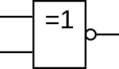
The XNOR gate with inputs A and B implements the logical expression .

Hardware description
XNOR gates are represented in most TTL and CMOS IC families. The standard 4000 series CMOS IC is the 4077, and the TTL IC is the 74266 (although an open-collector implementation). Both include four independent, two-input, XNOR gates. The (now obsolete) 74S135 implemented four two-input XOR/XNOR gates or two three-input XNOR gates.
Both the TTL 74LS implementation, the 74LS266, as well as the CMOS gates (CD4077, 74HC4077 and 74HC266 and so on) are available from most semiconductor manufacturers such as Texas Instruments or NXP, etc.[2] They are usually available in both through-hole DIP and SOIC formats (SOIC-14, SOC-14 or TSSOP-14).
Datasheets are readily available in most datasheet databases and suppliers.
Pinout
Both the 4077 and 74x266 devices (SN74LS266, 74HC266, 74266, etc.) have the same pinout diagram, as follows:
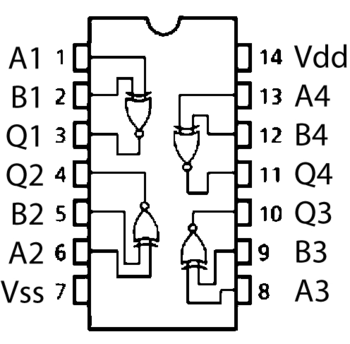
Pinout diagram of the 74HC266N, 74LS266 and CD4077 quad XNOR plastic dual in-line package 14-pin package (PDIP-14) ICs.
- Input A1
- Input B1
- Output Q1 (high if and only if A1 and B1 have the same logic level)
- Output Q2
- Input B2
- Input A2
- Vss (GND) common power and signal ground pin
- Input A3
- Input B3
- Output Q3
- Output Q4
- Input B4
- Input A4
- Vdd for CMOS (Vcc for TTL) positive power supply (see datasheets for acceptable voltage ranges)
Alternatives
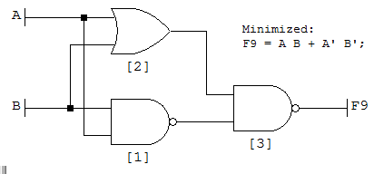
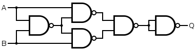
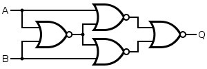
If no specific XNOR gates are available, one can be made from NAND gates or NOR gates in the configurations shown below. In fact, any logic gate can be made from combinations of only NAND gates or only NOR gates. Two possible configurations constructed from NAND gates and two possible configurations constructed from NOR gates are shown below.
| Desired gate | NAND construction | NOR construction |
|---|---|---|
 |  |  |
 | 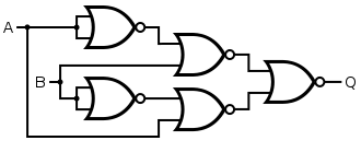 |
For the NAND constructions, the lower arrangement offers the advantage of a shorter propagation delay (the time delay between an input changing and the output changing). For the NOR constructions, the upper arrangement requires fewer gates.
More than two inputs
Although other gates (OR, NOR, AND, NAND) are available from manufacturers with three or more inputs per gate, this is not strictly true with XOR and XNOR gates. However, extending the concept of the binary logical operation to three inputs, the SN74S135 with two shared "C" and four independent "A" and "B" inputs for its four outputs, was a device that followed the truth table:
| Input | Output | ||
|---|---|---|---|
| A | B | C | Y |
| L | L | L | L |
| L | L | H | H |
| L | H | L | H |
| L | H | H | L |
| H | L | L | H |
| H | L | H | L |
| H | H | L | L |
| H | H | H | H |
Note that this is effectively Y = ((A XOR B) XOR C). It does not implement a logical "equivalence" function, unlike two-input Exclusive OR gates; for example its output is Low when all inputs are Low. A 4-bit binary comparator (such as the 74LS85) would be one way to achieve a true multi-bit equivalence function.
See also
| Wikimedia Commons has media related to XNOR gates. |
References
- ↑ "Exclusive-NOR Gate Tutorial". Retrieved 6 May 2018.
- ↑ "XNOR Logic Gates". Retrieved 6 May 2018.
 | ||


