Two-dimensional materials
2D Materials, sometimes referred to as single layer materials, are crystalline materials consisting of a single layer of atoms. These materials have found use in applications such as photovoltaics, semiconductors, electrodes and water purification.
2D materials can generally be categorised as either 2D allotropes of various elements or compounds (consisting of two or more covalently bonding elements).[1] The elemental 2D materials generally carry the -ene suffix in their names while the compounds have -ane or -ide suffixes. Layered combinations of different 2D materials are generally called van der Waals heterostructures.
The efficient integration of 2D functional layers with three-dimensional (3D) systems remains a significant challenge, limiting device performance and circuit design.[2]
Some 700 2D materials have been predicted to be stable, although many remain to be synthesized.[3][4] The global market for 2D materials is expected to reach US$390 million by 2025, mostly for graphene in the semiconductor, electronics, battery energy and composite materials markets.[5][6]
History
The first 2D material, graphene, a single layer of graphite, was isolated in 2004. Thereafter many other 2D materials were identified.
The first MXene was discovered in 2011 at Drexel University.
2D allotropes
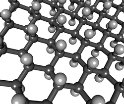
Graphene
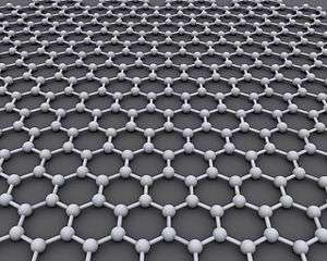
Graphene is a crystalline allotrope of carbon in the form of a nearly transparent (to visible light) one atom thick sheet. It is hundreds of times stronger than most steels by weight.[7] It has the highest known thermal and electrical conductivity, displaying current densities 1,000,000 times that of copper.[8] It was first produced in 2004.[9]
Andre Geim and Konstantin Novoselov won the 2010 Nobel Prize in Physics "for groundbreaking experiments regarding the two-dimensional material graphene". They first produced it by lifting graphene flakes from bulk graphite with adhesive tape and then transferring them onto a silicon wafer.[10]
Graphyne
Graphyne is another 2-dimensional carbon allotrope whose structure is similar to graphene's. It can be seen as a lattice of benzene rings connected by acetylene bonds. Depending on the content of the acetylene groups, graphyne can be considered a mixed hybridization, spn, where 1 < n < 2,[11][12] and versus graphene's (pure sp2) and diamond (pure sp3).
First-principle calculations using phonon dispersion curves and ab-initio finite temperature, quantum mechanical molecular dynamics simulations showed graphyne and its boron nitride analogues to be stable.[13]
The existence of graphyne was conjectured before 1960.[14] It has not yet been synthesized. However, graphdiyne (graphyne with diacetylene groups) was synthesized on copper substrates.[15] Recently it has been claimed to be a competitor for graphene, due to the potential of direction-dependent Dirac cones.[16][17]
Borophene
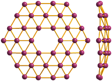
36° borophene, front and side view
Borophene is a proposed crystalline allotrope of boron. One unit consists of 36 atoms arranged in a 2-dimensional sheet with a hexagonal hole in the middle.[18][19] Borophene has also been synthesized, but with a different crystal structure.[20]
Germanene
Germanene is a two-dimensional allotrope of germanium, with a buckled honeycomb structure.[21] Experimentally synthesized germanene exhibits a honeycomb structure. This honeycomb structure consists of two hexagonal sub-lattices that are vertically displaced by 0.2 A from each other.[22]
Silicene
Silicene is a two-dimensional allotrope of silicon, with a hexagonal honeycomb structure similar to that of graphene.
Si2BN
In 2016 researchers predicted a 2d hexagonal, metallic allotrope of Si2BN with only sp2 bonds.[23]
Stanene
Stanene is a predicted topological insulator that may display dissipationless currents at its edges near room temperature. It is composed of tin atoms arranged in a single layer, in a manner similar to graphene.[24] Its buckled structure leads to high reactivity against common air pollutions such as NOx and COx and is able to trap and dissociate them at low temperature.[25]
Phosphorene
Phosphorene is a 2-dimensional, crystalline allotrope of phosphorus. Its mono-atomic hexagonal structure makes it conceptually similar to graphene. However, phosphorene has substantially different electronic properties; in particular it possesses a nonzero band gap while displaying high electron mobility.[26] This property potentially makes it a better semiconductor than graphene.[27] The synthesis of phosphorene mainly consists of micromechanical cleavage or liquid phase exfoliation methods. The former has a low yield while the latter produce free standing nanosheets in solvent and not on the solid support. The bottom up approaches like chemical vapor deposition are still blank because of its high reactivity. Therefore, in the current scenario, the most effective method for large area fabrication of thin films of phosphorene consists of wet assembly techniques like Langmuir-Blodgett involving the assembly followed by deposition of nanosheets on solid supports[28]
Bismuthene
Bismuthene, the two-dimensional allotrope of bismuth, was synthesized on silicon carbide in 2016[29] and is predicted to be a topological insulator. At first glance the system is similar to graphene, as the Bi atoms arrange in a honeycomb lattice. However the bandgap is as large as 800mV due to the large spin-orbit-coupling of the Bi atoms and their interaction with the substrate. Thus, room-temperature applications of the quantum spin Hall effect come into reach.
Molybdenite
Metals
Single and double atom layers of platinum in a two-dimensional film geometry has been demonstrated.[30][31] These atomically thin platinum films are epitaxially grown on graphene[30] which imposes a compressive strain that modifies the surface chemistry of the platinum, while also allowing charge transfer through the graphene.[31] Single atom layer of palladium with the thickness down to 2.6 Å,[32] and rhodium with the thickness of less than 4 Å [33] have also been synthesized and characterized with atomic force microscopy and transmission electron microscopy.
2D alloys
Two-dimensional alloys is single atomic layer of alloy that is incommensurate with underlying substrate. The 2D ordered alloy of Pb and Sn has been synthesized and characterized with scanning tunneling microscopy and low-energy electron diffraction in 2003.[34] Moreover, the 2D all proportional solid solution alloy of Pb and Bi has been synthesized in 2011.[35]
2D supracrystals
The supracrystals of 2D materials have been proposed and theoretically simulated.[36][37] These monolayer crystals are built of supra atomic periodic structures where atoms in the nodes of the lattice are replaced by symmetric complexes. For example, in the hexagonal structure of graphene patterns of 4 or 6 carbon atoms would be arranged hexagonally instead of single atoms, as the repeating node in the unit cell.
3D-topological structures (foams, aerogel substances and materials)
Aerographite
Aerogel
Nanogel
Carbon nanofoam
Compounds
Graphane
Graphane is a polymer of carbon and hydrogen with the formula unit (CH)
n where n is large. Graphane is a form of fully hydrogenated (on both sides) graphene.[38] Partial hydrogenation is then hydrogenated graphene.[39]
Graphane's carbon bonds are in sp3 configuration, as opposed to graphene's sp2 bond configuration. Thus graphane is a two-dimensional analog of cubic diamond.
The first theoretical description of graphane was reported in 2003[40] and its preparation was reported in 2009.
Graphane can be formed by electrolytic hydrogenation of graphene, few-layer graphene or high-oriented pyrolytic graphite. In the last case mechanical exfoliation of hydrogenated top layers can be used.[41]
p-doped graphane is postulated to be a high-temperature BCS theory superconductor with a Tc above 90 K.[42]
Hexagonal boron nitride
-side-3D-balls.png)
Properties
Structural
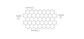
2D boron nitride is an sp2 conjugated compound that forms a honeycomb structure of alternating boron and nitrogen atoms with a lattice spacing of 1.45Å.[43][44] It adopts the hexagonal (h-BN) allotrope of the three possible crystalline forms of boron nitride because it is the most ubiquitous and stable structure.[44] Boron nitride nanosheets contain two different edges. In the armchair edge structure, the edge consists of either boron or nitrogen atoms.[44] In the zig-zag edge structure, the edge consists of alternating boron and nitrogen atoms.[44] These 2D structures can stack on top of each other and are held by Van der Waal forces to form what is called few-layer boron nitride nanosheets.[44][45] In these structures, the boron atoms of one sheet are positioned on top or below the nitrogen atoms due to electron deficient nature of boron and electron rich nature of nitrogen, respectively.[44][45] Due to several similar structural similarities with graphene, boron nitride nanosheets are considered graphene analogs, often called “white graphene".[45][46]
Boron nanosheets (BNNS) defined as single or few layers of boron nitride[44][46][47] whose aspect ratio is small.[44] However, there are a couple variations of 2D boron nitride structure.[44] Boron nitride nanoribbons (BNNR) are boron nitride nanosheets with significant edge effects[45] and have widths that are smaller than 50 nanometers.[44][48] Boron nitride nanomeshes (BNNM) are boron nitride nanosheets that are placed upon specific metal substrates.[45]
Electrical
Boron nitride nanosheets have a wide bandgap that ranges from 5 to 6 eV[44][45][46] and can be changed by the presence of Stone-Wales defects within the structure,[45] by doping[45] or functionalization,[45] or by changing the number of layers.[43][45] Due to this large bandgap and tunability as well as its surface flatness,[43] boron nitride nanosheets are considered to be an excellent electric insulators and are often used as dielectrics in electrical devices.[45][46][47][48]
Thermal
2D boron nitride structures are excellent thermal conductors,[44][45][46] with a thermal conductivity range of 100-270 W/mK.[43][44] It has been suggested that single layer boron nitride nanosheets have a greater thermal conductivity[43][45] than other forms of boron nitride nanosheets due to decreased phonon scattering[45] from subsequent layers.
The thermal stability of boron nitride nanosheets is very high due to the high thermal stability properties of hexagonal boron nitride.[43][44][46][49] As single layer and few-layer boron nitride nanosheets begin to oxidize and lose their electrical properties at 800 °C, they are excelle
Synthesis
CVD
Chemical vapor deposition is a popular synthesis method to produce boron nitride because it is a highly controllable process that produces high quality and defect free monolayer and few-layer boron nitride nanosheets.[45][46][47][48][50] In the majority of CVD methods, boron and nitride precursors react with a metal substrate at high temperature.[45][46] This allows for nanosheets of a large area as the layers grow uniformly on the substrate.[45][46][49] There is a wide range of boron and nitride precursors such as borazine and selection of these precursors depend on factors such as toxicity,[45] stability,[44][45] reactivity,[45] and the nature of the CVD method.[44][45][46][48] However, despite the high quality of the nanosheets synthesized by chemical vapor deposition, it is not a good method for the large scale production of boron nitride nanosheets for applications.[50]
Mechanical cleavage
While there are several mechanical cleaving methods to produce boron nitride nanosheets, they employ the same principle: using shear forces to break the Van der Waals interactions between the layers of boron nitride.[44] The advantage of mechanical cleavage is that the nanosheets isolated from these techniques have few defects and retain the lateral size of the original substrate.[44][45]
Inspired by its use in the isolation of graphene, micromechanical cleavage, also known as the Scotch-tape method, has been used to consistently isolate few-layer and monolayer boron nitride nanosheets by subsequent exfoliation of the beginning material with adhesive tape.[44][45][47][50] However, the disadvantage of this technique is that it is not scalable for large scale production.[44][45]
Ball milling is another technique used to mechanically exfoliate boron nitride sheets from the parent substrate.[43][44][45][46][47][48][51][50] In this process, shear forces are applied on the face of bulk boron nitride by rolling balls, which break the Van der Waal interactions between each layer.[44][45][48][50] While the ball milling technique may allow for large quantities of boron nitride nanosheets, it does not allow for control the size or the number of layers of the resulting nanosheets.[44][45] Furthermore, these nanosheets have more defects due to the aggressive nature of this technique.[43][50] However, improvements such as the addition of a milling agent such as benzyl benzoate[44][50] or the use of smaller balls[44] has allowed for a greater yield of higher quality nanosheets.[44][50]
Boron nitride nanosheets have also been isolated by using a vortex fluidic device, which uses centripetal force to shear off layers of boron nitride.[50]
Unzipping of boron nitride nanotubes
Boron nitride nanosheets may also be synthesized by the unzipping of boron nitride nanotubes (BNNT).[44][45][50] These nanotubes can be made into sheets by breaking the bonds connecting the N and B atoms by potassium intercalation[44][45][50] or by etching by plasma or an inert gas.[44][45][50] The unzipping of boron nitride nanotubes by plasma can be used to control the size of the nanosheets, but it produces semiconducting boron nitride nanosheets.[50] The potassium intercalation method produces a low yield of nanosheets as boron nitride is resistive to the effects of intercalants.[45]
Solvent exfoliation and sonication
Solvent exfoliation is often used in tandem with sonication to break the weak Van der Waals interactions present in bulk boron nitride to isolate large quantities of boron nitride nanosheets.[44][45][50] Polar solvents such as isopropyl alcohol[45] and DMF[52] have been found to be more effective in exfoliating boron nitride layers than nonpolar solvents because these solvents possess a similar surface energy to the surface energy of boron nitride nanosheets.[44] Combinations of different solvents also exfoliate boron nitride better than when the solvents were used individually.[44] However, many solvents that can be used to exfoliate boron nitride are fairly toxic and expensive.[50] Common solvents such as water and isopropyl alcohol have been determined to be comparable to these toxic polar solvents in exfoliating boron nitride sheets.[44][52]
Chemical functionalization and sonication
Chemical functionalization of boron nitride involves attaching molecules onto the outer and inner layers of bulk boron nitride.[45] There are three types of functionalization that can be done to boron nitride: covalent functionalization, ionic functionalization, or non covalent functionalization.[44] Layers are then exfoliated by placing the functionalized boron nitride into a solvent and allow the solvation force between the attached groups and the solvent to overcome the Van der Waal forces present in each layer.[50] This method is slightly different than solvent exfoliation as solvent exfoliation relies on the similarities between the surface energies of the solvent and boron nitride layers to overcome the Van der Waals interactions.
Solid State Reactions
The reaction of a mixture of boron and nitrogen precursors at high temperature can produce boron nitride nanosheets.[44][50] In one method, boric acid and urea were reacted together at 900˚C.[48][50] The numbers of layers of these nanosheets were controlled by the urea content as well as the temperature[50]
Borocarbonitrides
See also: graphene, boron nitride
Properties
Structural
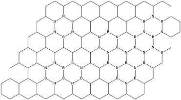
Borocarbonitrides are two-dimensional compounds that are synthesized such that they contain boron, nitrogen, and carbon atoms in a ratio BxCyNz.[53][54] Borocarbonitrides are distinct from B,N co-doped graphene in that the former contains separate boron nitride
and graphene domains as well as rings with B-C, B-N, C-N, and C-C bonds.[55] These compounds generally have a high surface area, but borocarbonitrides synthesized from a high surface area carbon material, urea, and boric acid tend to have the highest surface areas.[53][56][48] This high surface area coupled with the presence of Stone-Wales defects in the structure of borocarbonitrides also allows for high absorption of CO2 and CH4, which may make borocarbonitride compounds a useful material in sequestering these gases.[53][56]
Electrical
The band gap of borocarbonitrides range from 1.0-3.9eV[53] and is dependent on the content of the carbon and boron nitride domains as they have different electrical properties.[53] Borocarbonitrides with a high carbon content have lower bandgaps[54] whereas those with higher content of boron nitride domains have higher band gaps.[53] Borocarbonitrides synthesized in gas or solid reactions also tend to have large bandgaps and are more insulating in character.[53] The wide range of composition of boronitrides allows for the tuning of the bandgap, which when coupled with its high surface area and Stone-Wales defects may make boronitrides a promising material in electrical devices.[54][16]
Synthesis
Solid state reaction
A high surface area carbon material such as activated charcoal, boric acid, and urea are mixed together and then heated at high temperatures to synthesize borocarbonitride.[54] The composition of the resulting compounds may be changed by varying the concentration of the reagents as well as the temperature.[53]
Gas phase synthesis
In chemical vapor deposition, boron, nitrogen, and carbon precursors react at high heat and are deposited onto a metal substrate.[53] Varying the concentration of precursors and the selection of certain precursors will give different ratios of boron, nitrogen, and carbon in the resulting borocarbonitride compound.[54]
Borocarbonitride composites
Borocarbonitride can also be synthesized by random stacking of boronitride and graphene domains through covalent interactions[54] or through liquid interactions.[53] In the first method, graphene and boron nitride sheets are functionalized and then are reacted to form layers of borocarbonitride.[54] In the second method, boron nitride and graphite powder are dissolved in isopropanol and dimethylformamide, respectively, and then sonicated.[54] This is then exfoliated to isolate borocarbonitride layers.
Germanane
Germanane is a single-layer crystal composed of germanium with one hydrogen bonded in the z-direction for each atom.[57] Germanane’s structure is similar to graphane,[58] Bulk germanium does not adopt this structure. Germanane is produced in a two-step route starting with calcium germanide. From this material, the calcium (Ca) is removed by de-intercalation with HCl to give a layered solid with the empirical formula GeH.[59] The Ca sites in Zintyl-phase CaGe
2 interchange with the hydrogen atoms in the HCl solution, producing GeH and CaCl2.
Transition metal Di-chalcogenides (TMDCs)
Molybdenum disulfide
2, with Mo in blue and S in yellow
Properties
Structural
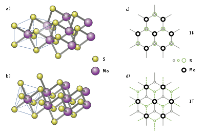
Molybdenum disulfide monolayers consist of a unit of one layer of molybdenum atoms covalently bonded to two layers of sulfur atoms. While bulk molybdenum sulfide exists as 1T, 2H, or 3R polymorphs, molybdenum disulfide monolayers are found only in the 1T or 2H form.[55] The 2H form adopts a trigonal prismatic geometry[60] while the 1T form adopts an octahedral or trigonal antiprismatic geometry.[55] Molybdenum monolayers can also can be stacked due to Van der Waals interactions between each layer.
Electrical
The electrical properties of molybdenum sulfide in electrical devices depends on factors such as the number of layers,[61] the synthesis method,[55] the nature of the substrate on which the monolayers are placed on,[62] and mechanical strain.[63]
As the number of layers decrease, the band gap begins to increase from 1.2eV in the bulk material up to a value of 1.9eV for a monolayer.[48] Odd number of molybdenum sulfide layers also produce different electrical properties than even numbers of molybednum sulfide layers due to cyclic stretching and releasing present in the odd number of layers.[64] Molybdenum sulfide is a p-type material, but it shows ambipolar behavior when molybdenum sulfide monolayers that were 15 nm thick were used in transistors.[48] However, most electrical devices containing molybdenum sulfide monolayers tend to show n-type behavior.[60][22]
The band gap of molybdenum disulfide monolayers can also be adjusted by applying mechanical strain[63] or an electrical field.[48] Increasing mechanical strain shifts the phonon modes of the molybdenum sulfide layers.[63] This results in a decrease of the band gap and metal-to-insulator transition.[55] Applying an electric field of 2-3Vnm−1 also decreases the indirect bandgap of molybdenum sulfide bilayers to zero.[55]
Solution phase lithium intercalation and exfolation of bulk molybdenum sulfide produces molybdenum sulfide layers with metallic and semiconducting character due to the distribution of 1T and 2H geometries within the material.[48][55] This is due to the two forms of molybdenum sulfide monolayers having different electrical properties. The 1T polymorph of molybednum sulfide is metallic in character while the 2H form is more semiconducting.[60] However, molybdenum disulfide layers produced by electrochemical lithium intercalation are predominantly 1T and thus metallic in character as there is no conversion to the 2H form from the 1T form.[55]
Thermal
The thermal conductivity of molybdenum disulfide monolayers at room temperature is 34.5W/mK[65] while the thermal conductivity of few-layer molybdenum disulfide is 52W/mK.[65] The thermal conductivity of graphene, on the other hand, is 5300W/mK.[65] Due to the rather low thermal conductivity of molybdenum disulfide nanomaterials, it is not as promising material for high thermal applications as some other 2D materials.
Synthesis
Exfoliation
Exfoliation techniques for the isolating of molybdenum disulfide monolayers include mechanical exfoliation,[55] solvent assisted exfoliation,[60] and chemical exfolation.[48]
Solvent assisted exfoliation is done by sonicating bulk molybdenum disulfide in an organic solvent such as isopropanol and N-methyl-2-pyrrolidone, which disperses the bulk material into nanosheets as the Van der Waals interactions between the layers in the bulk materaial are broken.[55] The amount of nanosheets produced is controlled by the sonication time,[60] the solvent-molybdenum disulfide interactions,[55] and the centrifuge speed.[55] Compared to other exfoliation techniques, solvent assisted exfoliation is the simplest method for large scale production of molybdenum disulfide nanosheets.[66]
The micromechanical exfoliation of molybdenum disulfide was inspired by the same technique used in the isolation of graphene nanosheets.[66] Micromechanical exfoliation allows for low defect molybdenum disulfide nanosheets but is not suitable for large scale production due to low yield.[60]
Chemical exfoliation involves functionalizing molybdenum difsulfide and then sonicating to disperse the nanosheets.[66] The most notable chemical exfoliation technique is lithium intercalation in which lithium is intercalated into bulk molybdenum disulfide and then dispersed into nanosheets by the addition of water.[48]
Chemical vapor deposition (CVD)
Chemical vapor deposition of molybdenum disulfide nanosheets involves reacting molybdenum and sulfur precursors on a substrate at high temperatures.[66] This technique is often used in the preparing electrical devices with molybdenum disulfide components because the nanosheets are applied directly on the substrate; unfavorable interactions between the substrate and the nanosheets that would have occurred had they been separately synthesized are decreased.[60] In addition, since the thickness and area of the molybdenum disulfide nanosheets can be controlled by the selection of specific precursors, the electrical properties of the nanosheets can be tuned.[60]
Laser ablation
Pulsed laser deposition involves the thinning of bulk molybdenum disulfide by laser to produce single or multi-layer molybdenum disulfide nanosheets.[55] This allows for synthesis of molybdenum disulfide nanosheets with a defined shape and size.[48] The quality of the nanosheets are determined by the energy of the laser and the irradation angle.[66]
Lasers can also be used to form molybdenum disulfide nanosheets from molybdenum disulfide fullerene-like molecules.[67]
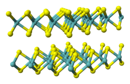
Tungsten diselenide
Tungsten diselenide is an inorganic compound with the formula WSe
2. The compound adopts a hexagonal crystalline structure similar to molybdenum disulfide. Every tungsten atom is covalently bonded to six selenium ligands in a trigonal prismatic coordination sphere, while each selenium is bonded to three tungsten atoms in a pyramidal geometry. The tungsten – selenium bond has a bond distance of 2.526 Å and the distance between selenium atoms is 3.34 Å.[68] Layers stack together via van der Waals interactions. WSe
2 is a stable semiconductor in the group-VI transition metal dichalcogenides. The electronic bandgap of WSe
2 can be tuned by mechanical strain[69] which can also allow for conversion of the band type from indirect-to-direct in a WSe
2 bilayer.[70]
Hafnium Disulphide
Hafnium Disulphide is a group IVB TMD with formula HfS
2. Like other TMDs, it possess a layered structure with strong covalent bonding between the Hf and S atoms in a layer and weak Van der Wall forces between layers. The compound has CdI
2 type structure and is an indirect band gap semiconducting material. The interlayer spacing between the layers is 0.56 nm, which is small compared to group VIB TMDs like MoS
2, making it difficult to cleave its atomic layers. However, recently its crystals with large interlayer spacing has grown using a chemical vapor transport route.[71] These crystals exfoliate in solvents like N-Cyclohexyl-2-pyrrolidone (CHP) in a time of just some minutes resulting in a high-yield production of its few-layers resulting in increase of its indirect bandgap from 0.9 eV to 1.3 eV. As an application in electronics, its field-effect transistors has been realised using its few layers as a conducting channel material offering a high current modulation ratio larger than 10000 at room temperature. Therefore, group IVB TMDs also holds potential applications in the field of opto-electronics.
MXenes
MXenes are layered transition metal carbides and carbonitrides with general formula of Mn+1XnTx, where M stands for early transition metal, X stands for carbon and/or nitrogen and Tx stands for surface terminations (mostly =O, -OH or -F). MXenes have high electric conductivity (10000-1500 Scm−1) combined with hydrophilic surfaces that can be tuned with solvents. This materials show promise in energy storage applications and composites. They are synthesized from ceramic precursor MAX phases by removing the single atomic layer "A" where M stands for Ti, Mo, W, Nb, Zr, Hf, V, Cr, Ta, Sc, A stands for Al, Si, and X stands for C, N. Millions of predicted solid solutions of these materials have been identified and 30+ MXenes have been synthesized.
Organic
Ni3(HITP)2 is an organic, crystalline, structurally tunable electrical conductor with a high surface area. HITP is an organic chemical (2,3,6,7,10,11-hexaaminotriphenylene). It shares graphene's hexagonal honeycomb structure. Multiple layers naturally form perfectly aligned stacks, with identical 2-nm openings at the centers of the hexagons. Room temperature electrical conductivity is ~40 S cm−1, comparable to that of bulk graphite and among the highest for any conducting metal-organic frameworks (MOFs). The temperature dependence of its conductivity is linear at temperatures between 100 K and 500 K, suggesting an unusual charge transport mechanism that has not been previously observed in organic semiconductors.[72]
The material was claimed to be the first of a group formed by switching metals and/or organic compounds. The material can be isolated as a powder or a film with conductivity values of 2 and 40 S cm−1, respectively.[73]
Combinations
A 2015 study stacked two different TMD layers onto graphene. This composite displayed negative differential resistance – applying more voltage to the device reduced the current flowing through it.[26] A recent study combined graphene and hexagonal boron nitride to form a planar two-dimensional material.[74] This combination displayed variety of structural formations that potentially varies the electrical, thermal and optical properties.
Characterization of 2D materials
Microscopy techniques such as transmission electron microscopy,[75][76][77] scanning probe microscopy,[48] scanning tunneling microscopy,[75] and atomic force microscopy[75][77][48] are used to characterize the thickness and size of the 2D materials. Electrical properties and structural properties such as composition and defects are characterized by raman spectroscopy,[75][77][48] x-ray diffraction,[75][77] and x-ray photoelectron spectroscopy.[55]
Applications
As of 2014, none of these materials has been used for large scale commercial applications (with the possible exception of graphene). Despite this, many are under close consideration for a number of industries, in areas including electronics and optoelectronics, sensors, biological engineering, filtration, lightweight/strong composite materials, photovoltaics, medicine, quantum dots, thermal management, ethanol distillation and energy storage,[78] cryptography[79] and have enormous potential.
Graphene has been the most studied. In small quantities it is available as a powder and as a dispersion in a polymer matrix, or adhesive, elastomer, oil and aqueous and non-aqueous solutions. The dispersion is claimed to be suitable for advanced composites, paints and coatings, lubricants, oils and functional fluids, capacitors and batteries, thermal management applications, display materials and packaging, inks and 3D-printers’ materials, and barriers and films.[80][81]
Biological applications
Research on 2D nanomaterials is still in its infancy, with the majority of research focusing on elucidating the unique material characteristics and few reports focusing on biomedical applications of 2D nanomaterials.[82] Nevertheless, recent rapid advances in 2D nanomaterials have raised important yet exciting questions about their interactions with biological moieties. 2D nanoparticles such as carbon-based 2D materials, silicate clays, transition metal dichalcogenides (TMDs), and transition metal oxides (TMOs) provide enhanced physical, chemical, and biological functionality owing to their uniform shapes, high surface-to-volume ratios, and surface charge.
Two-dimensional (2D) nanomaterials are ultrathin nanomaterials with a high degree of anisotropy and chemical functionality.[83] 2D nanomaterials are highly diverse in terms of their mechanical, chemical, and optical properties, as well as in size, shape, biocompatibility, and degradability.[84][85] These diverse properties make 2D nanomaterials suitable for a wide range of applications, including drug delivery, imaging, tissue engineering, and biosensors, among others.[86] However, their low-dimension nanostructure gives them some common characteristics. For example, 2D nanomaterials are the thinnest materials known, which means that they also possess the highest specific surface areas of all known materials. This characteristic makes these materials invaluable for applications requiring high levels of surface interactions on a small scale. As a result, 2D nanomaterials are being explored for use in drug delivery systems, where they can adsorb large numbers of drug molecules and enable superior control over release kinetics.[87] Additionally, their exceptional surface area to volume ratios and typically high modulus values make them useful for improving the mechanical properties of biomedical nanocomposites and nanocomposite hydrogels, even at low concentrations. Their extreme thinness has been instrumental for breakthroughs in biosensing and gene sequencing. Moreover, the thinness of these molecules allows them to respond rapidly to external signals such as light, which has led to utility in optical therapies of all kinds, including imaging applications, photothermal therapy (PTT), and photodynamic therapy (PDT).
Despite the rapid pace of development in the field of 2D nanomaterials, these materials must be carefully evaluated for biocompatibility in order to be relevant for biomedical applications.[88] The newness of this class of materials means that even the relatively well-established 2D materials like graphene are poorly understood in terms of their physiological interactions with living tissues. Additionally, the complexities of variable particle size and shape, impurities from manufacturing, and protein and immune interactions have resulted in a patchwork of knowledge on the biocompatibility of these materials.
References
- ↑ Garcia, J. C.; de Lima, D. B.; Assali, L. V. C.; Justo, J. F. (1324). "Group IV graphene- and graphane-like nanosheets". J. Phys. Chem. C. 115 (27): 13242–13246. arXiv:1204.2875. doi:10.1021/jp203657w.
- ↑ Xu, Yang; Cheng, Cheng; Du, Sichao; Yang, Jianyi; Yu, Bin; Luo, Jack; Yin, Wenyan; Li, Erping; Dong, Shurong; Ye, Peide; Duan, Xiangfeng (2016). "Contacts between Two- and Three-Dimensional Materials: Ohmic, Schottky, and p–n Heterojunctions". ACS Nano. 10 (5): 4895–4919. doi:10.1021/acsnano.6b01842. PMID 27132492.
- ↑ Ashton, M.; Paul, J.; Sinnott, S. B.; Hennig, R. G. (1061). "Topology-Scaling Identification of Layered Solids and Stable Exfoliated 2D Materials". Phys. Rev. Lett. 118 (10): 106101. arXiv:1610.07673. Bibcode:2017PhRvL.118j6101A. doi:10.1103/PhysRevLett.118.106101. PMID 28339265.
- ↑ "MaterialsWeb.org - Databases of Structural, Electronic, and Thermodynamic data for 2D and 3D Materials".
- ↑ "Graphene-Info Market Report". Graphene-info. June 2015. Retrieved 16 June 2015.
- ↑ "Global Demand for Graphene after Commercial Production to be Enormous". AZONANO.com. 28 February 2014. Retrieved 24 July 2014.
- ↑ Andronico, Michael (14 April 2014). "5 Ways Graphene Will Change Gadgets Forever". Laptop.
- ↑ "Graphene properties". www.graphene-battery.net. 2014-05-29. Retrieved 2014-05-29.
- ↑ "This Month in Physics History: October 22, 2004: Discovery of Graphene". APS News. Series II. 18 (9): 2. 2009.
- ↑ "The Nobel Prize in Physics 2010". The Nobel Foundation. Retrieved 2013-12-03.
- ↑ Heimann, R.B.; Evsvukov, S.E.; Koga, Y. (1997). "Carbon allotropes: a suggested classification scheme based on valence orbital hybridization". Carbon. 35 (10–11): 1654–1658. doi:10.1016/S0008-6223(97)82794-7.
- ↑ Enyashin, Andrey N.; Ivanovskii, Alexander L. (2011). "Graphene Allotropes". Physica Status Solidi B. 248 (8): 1879–1883. Bibcode:2011PSSBR.248.1879E. doi:10.1002/pssb.201046583.
- ↑ Özçelik, V. Ongun; S. Ciraci (January 10, 2013). "Size Dependence in the Stabilities and Electronic Properties of α-Graphyne and Its Boron Nitride Analogue". The Journal of Physical Chemistry C. 117 (5): 2175–2182. doi:10.1021/jp3111869. hdl:11693/11999.
- ↑ Balaban, AT; Rentia, CC; Ciupitu, E. (1968). Rev. Roum. Chim. 13: 231.
- ↑ Guoxing Li; Yuliang Li; Huibiao Liu; Yanbing Guo; Yongjun Li; Daoben Zhu (2010). "Architecture of graphdiyne nanoscale films". Chemical Communications. 46 (19): 3256–3258. doi:10.1039/B922733D. PMID 20442882.
- 1 2 Gopalakrishnan, K.; Moses, Kota; Govindaraj, A.; Rao, C. N. R. (2013-12-01). "Supercapacitors based on nitrogen-doped reduced graphene oxide and borocarbonitrides". Solid State Communications. Special Issue: Graphene V: Recent Advances in Studies of Graphene and Graphene analogues. 175–176: 43–50. Bibcode:2013SSCom.175...43G. doi:10.1016/j.ssc.2013.02.005.
- ↑ Schirber, Michael (24 February 2012). "Focus: Graphyne May Be Better than Graphene". Physics. 5 (24): 24. Bibcode:2012PhyOJ...5...24S. doi:10.1103/Physics.5.24.
- ↑ "Will 'borophene' replace graphene as a better conductor of electrons?". KurzweilAI. February 5, 2014. Retrieved February 5, 2014.
- ↑ Piazza, Z. A.; Hu, H. S.; Li, W. L.; Zhao, Y. F.; Li, J.; Wang, L. S. (2014). "Planar hexagonal B36 as a potential basis for extended single-atom layer boron sheets". Nature Communications. 5: 3113. Bibcode:2014NatCo...5E3113P. doi:10.1038/ncomms4113. PMID 24445427.
- ↑ Mannix, AJ; Zhou, XF; Kiraly, B; Wood, JD; Alducin, D; Myers, BD; Liu, X; Fisher, BL; Santiago, U; Guest, JR; Yacaman, MJ; Ponce, A; Oganov, AR; Hersam, MC; Guisinger, NP (December 18, 2015). "Synthesis of borophenes: Anisotropic, two-dimensional boron polymorphs". Science. 350 (6267): 1513–1516. Bibcode:2015Sci...350.1513M. doi:10.1126/science.aad1080. PMC 4922135. PMID 26680195.
- ↑ Bampoulis, P.; Zhang, L.; Safaei, A.; van Gastel, R.; Poelsema, B.; Zandvliet, H. J. W. (2014). "Germanene termination of Ge2Pt crystals on Ge(110)". Journal of Physics: Condensed Matter. 26 (44): 442001. arXiv:1706.00697. Bibcode:2014JPCM...26R2001B. doi:10.1088/0953-8984/26/44/442001. PMID 25210978.
- 1 2 Lee, Kangho; Kim, Hye-Young; Lotya, Mustafa; Coleman, Jonathan N.; Kim, Gyu-Tae; Duesberg, Georg S. (2011-09-22). "Electrical Characteristics of Molybdenum Disulfide Flakes Produced by Liquid Exfoliation". Advanced Materials. 23 (36): 4178–4182. doi:10.1002/adma.201101013. ISSN 1521-4095. PMID 21823176.
- ↑ Andriotis, Antonis N. (2016-01-01). "Prediction of a new graphenelike". Physical Review B. 93 (8): 081413. Bibcode:2016PhRvB..93h1413A. doi:10.1103/PhysRevB.93.081413.
- ↑ Yuhara, J.; Fujii, Y.; Isobe, N.; Nakatake, M.; Lede, X.; Rubio, A.; Le Lay, G. (2018). "Large Area Planar Stanene Epitaxially Grown on Ag(111)". 2D Materials. 5 (2): 025002. Bibcode:2018TDM.....5b5002Y. doi:10.1088/2053-1583/aa9ea0.
- ↑ Takahashi, L.; Takahashi, K. (2015). "Low temperature pollutant trapping and dissociation over two-dimensional tin". Physical Chemistry Chemical Physics. 17 (33): 21394–21396. Bibcode:2015PCCP...1721394T. doi:10.1039/C5CP03382A. PMID 26226204.
- 1 2 Berger, Andy (July 17, 2015). "Beyond Graphene, a Zoo of New 2-D Materials". Discover Magazine. Retrieved 2015-09-19.
- ↑ Li, L.; Yu, Y.; Ye, G. J.; Ge, Q.; Ou, X.; Wu, H.; Feng, D.; Chen, X. H.; Zhang, Y. (2014). "Black phosphorus field-effect transistors". Nature Nanotechnology. 9 (5): 372–377. arXiv:1401.4117. Bibcode:2014NatNa...9..372L. doi:10.1038/nnano.2014.35. PMID 24584274.
- ↑ Ritu, Harneet (2016). "Large Area Fabrication of Semiconducting Phosphorene by Langmuir-Blodgett Assembly". Sci. Rep. 6: 34095. arXiv:1605.00875. Bibcode:2016NatSR...634095K. doi:10.1038/srep34095. PMC 5037434. PMID 27671093.
- ↑ Reis, Felix; Li, Gang; Dudy, Lenart; Bauernfiend, Maximilian; Glass, Stefan; Hanke, Werner; Thomale, Ronny; Schaefer, Joerg; Claessen, Ralph (July 21, 2017). "Bismuthene on a SiC substrate: A candidate for a high-temperature quantum spin Hall material". Science. 357 (6348): 287–290. arXiv:1608.00812. Bibcode:2017Sci...357..287R. doi:10.1126/science.aai8142. PMID 28663438.
- 1 2 Abdelhafiz, Ali; Vitale, Adam; Buntin, Parker; deGlee, Ben; Joiner, Corey; Robertson, Alex; Vogel, Eric M.; Warner, Jamie; Alamgir, Faisal M. (2018). "Epitaxial and atomically thin graphene–metal hybrid catalyst films: the dual role of graphene as the support and the chemically-transparent protective cap". Energy & Environmental Science. 11 (6): 1610–1616. doi:10.1039/c8ee00539g. ISSN 1754-5692.
- 1 2 Abdelhafiz, Ali; Vitale, Adam; Joiner, Corey; Vogel, Eric; Alamgir, Faisal M. (2015-03-16). "Layer-by-Layer Evolution of Structure, Strain, and Activity for the Oxygen Evolution Reaction in Graphene-Templated Pt Monolayers". ACS Applied Materials & Interfaces. 7 (11): 6180–6188. doi:10.1021/acsami.5b00182. ISSN 1944-8244.
- ↑ Yin, Xi; Liu, Xinhong; Pan, Yung-Tin; Walsh, Kathleen A.; Yang, Hong (November 4, 2014). "Hanoi Tower-like Multilayered Ultrathin Palladium Nanosheets". Nano Letters. 14 (12): 7188–7194. Bibcode:2014NanoL..14.7188Y. doi:10.1021/nl503879a. PMID 25369350.
- ↑ Duan, Haohong; Yan, Ning; Yu, Rong; Chang, Chun-Ran; Zhou, Gang; Hu, Han-Shi; Rong, Hongpan; Niu, Zhiqiang; Mao, Junjie; Asakura, Hiroyuki; Tanaka, Tsunehiro; Dyson, Paul Joseph; Li, Jun; Li, Yadong (17 January 2014). "Ultrathin rhodium nanosheets". Nature Communications. 5: 3093. Bibcode:2014NatCo...5E3093D. doi:10.1038/ncomms4093. ISSN 2041-1723. PMID 24435210.
- ↑ Yuhara, J.; Schmid, M.; Varga, P. (2003). "A two-dimensional alloy of immiscible metals, The single and binary monolayer films of Pb and Sn on Rh(111)". Phys. Rev. B. 67 (19): 195407. Bibcode:2003PhRvB..67s5407Y. doi:10.1103/PhysRevB.67.195407.
- ↑ Yuhara, J.; Yokoyama, M.; Matsui, T. (2011). "Two-dimensional solid solution alloy of Bi-Pb binary films on Rh(111)". J. Appl. Phys. 110 (7): 074314–074314–4. Bibcode:2011JAP...110g4314Y. doi:10.1063/1.3650883.
- ↑ Kochaev, A. I.; Karenin, A.A.; Meftakhutdinov, R.M.; Brazhe, R.A. (2012). "2D supracrystals as a promising materials for planar nanoacoustoelectronics". Journal of Physics: Conference Series. 345 (1): 012007. Bibcode:2012JPhCS.345a2007K. doi:10.1088/1742-6596/345/1/012007.
- ↑ Brazhe, R. A.; Kochaev, A. I. (2012). "Flexural waves in graphene and 2D supracrystals". Physics of the Solid State. 54 (8): 1612–1614. Bibcode:2012PhSS...54.1612B. doi:10.1134/S1063783412080069.
- ↑ Sofo, Jorge O.; et al. (2007). "Graphane: A two-dimensional hydrocarbon". Physical Review B. 75 (15): 153401–4. arXiv:cond-mat/0606704. Bibcode:2007PhRvB..75o3401S. doi:10.1103/PhysRevB.75.153401.
- ↑ D. C. Elias; et al. (2009). "Control of Graphene's Properties by Reversible Hydrogenation: Evidence for Graphane". Science. 323 (5914): 610–3. arXiv:0810.4706. Bibcode:2009Sci...323..610E. doi:10.1126/science.1167130. PMID 19179524.
- ↑ Sluiter, Marcel; Kawazoe, Yoshiyuki (2003). "Cluster expansion method for adsorption: Application to hydrogen chemisorption on graphene". Physical Review B. 68 (8): 085410. Bibcode:2003PhRvB..68h5410S. doi:10.1103/PhysRevB.68.085410.
- ↑ A. M. Ilyin; et al. (2011). "Computer simulation and experimental study of graphane-like structures formed by electrolytic hydrogenation". Physica E. 43 (6): 1262–65. Bibcode:2011PhyE...43.1262I. doi:10.1016/j.physe.2011.02.012.
- ↑ G. Savini; et al. (2010). "Doped graphane: a prototype high-Tc electron-phonon superconductor". Phys Rev Lett. 105 (5): 059902. arXiv:1002.0653. Bibcode:2010PhRvL.105e9902S. doi:10.1103/physrevlett.105.059902.
- 1 2 3 4 5 6 7 8 Li, Lu Hua; Chen, Ying (2594). "Atomically Thin Boron Nitride: Unique Properties and Applications". Advanced Functional Materials. 26 (16): 2594–2608. arXiv:1605.01136. doi:10.1002/adfm.201504606. ISSN 1616-3028. Check date values in:
|year=(help) - 1 2 3 4 5 6 7 8 9 10 11 12 13 14 15 16 17 18 19 20 21 22 23 24 25 26 27 28 29 30 31 32 33 34 35 Bhimanapati, G. R.; Glavin, N. R.; Robinson, J. A. (2016-01-01). Francesca Iacopi, John J. Boeckl and Chennupati Jagadish, ed. Semiconductors and Semimetals. 2D Materials. 95. Elsevier. pp. 101–147.
- 1 2 3 4 5 6 7 8 9 10 11 12 13 14 15 16 17 18 19 20 21 22 23 24 25 26 27 28 29 30 31 32 33 34 Lin, Yi; Connell, John W. (2012-10-29). "Advances in 2D boron nitride nanostructures: nanosheets, nanoribbons, nanomeshes, and hybrids with graphene". Nanoscale. 4 (22): 6908–39. Bibcode:2012Nanos...4.6908L. doi:10.1039/c2nr32201c. ISSN 2040-3372. PMID 23023445.
- 1 2 3 4 5 6 7 8 9 10 11 Pakdel, Amir; Zhi, Chunyi; Bando, Yoshio; Golberg, Dmitri (2012-06-01). "Low-dimensional boron nitride nanomaterials". Materials Today. 15 (6): 256–265. doi:10.1016/S1369-7021(12)70116-5.
- 1 2 3 4 5 Wang, Xuebin; Zhi, Chunyi; Weng, Qunhong; Bando, Yoshio; Golberg, Dmitri (2013-01-01). "Boron Nitride Nanosheets: novel Syntheses and Applications in polymeric Composites". Journal of Physics: Conference Series. 471 (1): 012003. doi:10.1088/1742-6596/471/1/012003. ISSN 1742-6596.
- 1 2 3 4 5 6 7 8 9 10 11 12 13 14 15 16 17 18 Rao, C. N. R.; Ramakrishna Matte, H. S. S.; Maitra, Urmimala (2013-12-09). "Graphene Analogues of Inorganic Layered Materials". Angewandte Chemie International Edition. 52 (50): 13162–13185. doi:10.1002/anie.201301548. ISSN 1521-3773. PMID 24127325.
- 1 2 Li, Lu Hua; Cervenka, Jiri; Watanabe, Kenji; Taniguchi, Takashi; Chen, Ying (2014-02-25). "Strong Oxidation Resistance of Atomically Thin Boron Nitride Nanosheets". ACS Nano. 8 (2): 1457–1462. doi:10.1021/nn500059s. ISSN 1936-0851. PMID 24400990.
- 1 2 3 4 5 6 7 8 9 10 11 12 13 14 15 16 17 18 19 Wang, Zifeng; Tang, Zijie; Xue, Qi; Huang, Yan; Huang, Yang; Zhu, Minshen; Pei, Zengxia; Li, Hongfei; Jiang, Hongbo (2016-06-01). "Fabrication of Boron Nitride Nanosheets by Exfoliation". The Chemical Record. 16 (3): 1204–1215. doi:10.1002/tcr.201500302. ISSN 1528-0691. PMID 27062213.
- ↑ Li, Lu Hua; Chen, Ying; Behan, Gavin; Zhang, Hongzhou; Petravic, Mladen; Glushenkov, Alexey M. (2011-08-03). "Large-scale mechanical peeling of boron nitride nanosheets by low-energy ball milling". Journal of Materials Chemistry. 21 (32): 11862. doi:10.1039/c1jm11192b. ISSN 1364-5501.
- 1 2 Zhi, Chunyi; Bando, Yoshio; Tang, Chengchun; Kuwahara, Hiroaki; Golberg, Dimitri (2009-07-27). "Large-Scale Fabrication of Boron Nitride Nanosheets and Their Utilization in Polymeric Composites with Improved Thermal and Mechanical Properties". Advanced Materials. 21 (28): 2889–2893. doi:10.1002/adma.200900323. ISSN 1521-4095.
- 1 2 3 4 5 6 7 8 9 10 kumar, Nitesh; Moses, Kota; Pramoda, K.; Shirodkar, Sharmila N.; Mishra, Abhishek Kumar; Waghmare, Umesh V.; Sundaresan, A.; Rao, C. N. R. (2013-04-23). "Borocarbonitrides, BxCyNz". Journal of Materials Chemistry A. 1 (19): 5806. doi:10.1039/c3ta01345f. ISSN 2050-7496.
- 1 2 3 4 5 6 7 8 Rao, C. N. R.; Gopalakrishnan, K. (2016-10-31). "Borocarbonitrides, BxCyNz: Synthesis, Characterization, and Properties with Potential Applications". ACS Applied Materials & Interfaces. 9 (23): 19478–19494. doi:10.1021/acsami.6b08401. ISSN 1944-8244. PMID 27797466.
- 1 2 3 4 5 6 7 8 9 10 11 12 13 14 Rao, C. N. R; Maitra, Urmimala (2015-01-01). "Inorganic Graphene Analogs". Annual Review of Materials Research. 45 (1): 29–62. Bibcode:2015AnRMS..45...29R. doi:10.1146/annurev-matsci-070214-021141.
- 1 2 Raidongia, Kalyan; Nag, Angshuman; Hembram, K. P. S. S.; Waghmare, Umesh V.; Datta, Ranjan; Rao, C. N. R. (2010-01-04). "BCN: A Graphene Analogue with Remarkable Adsorptive Properties". Chemistry – A European Journal. 16 (1): 149–157. doi:10.1002/chem.200902478. ISSN 1521-3765. PMID 19946909.
- ↑ Bianco, E.; Butler, S.; Jiang, S.; Restrepo, O. D.; Windl, W.; Goldberger, J. E. (2013). "Stability and Exfoliation of Germanane: A Germanium Graphane Analogue". ACS Nano. 7 (5): 4414–21. doi:10.1021/nn4009406. hdl:1811/54792. PMID 23506286.
- ↑ Garcia, J. C.; de Lima, D. B.; Assali, L. V. C.; Justo, J. F. (1324). "Group IV graphene- and graphane-like nanosheets". J. Phys. Chem. C. 115 (27): 13242–13246. arXiv:1204.2875. doi:10.1021/jp203657w.
- ↑ "'Germanane' may replace silicon for lighter, faster electronics". KurzweilAI. Retrieved 2013-04-12.
- 1 2 3 4 5 6 7 8 Li, Xiao; Zhu, Hongwei (2015-03-01). "Two-dimensional MoS2: Properties, preparation, and applications". Journal of Materiomics. 1 (1): 33–44. doi:10.1016/j.jmat.2015.03.003.
- ↑ Mak, Kin Fai; Lee, Changgu; Hone, James; Shan, Jie; Heinz, Tony F. (2010). "Atomically ThinMoS2: A New Direct-Gap Semiconductor". Physical Review Letters. 105 (13): 136805. arXiv:1004.0546. Bibcode:2010PhRvL.105m6805M. doi:10.1103/physrevlett.105.136805. PMID 21230799.
- ↑ Najmaei, Sina; Zou, Xiaolong; Er, Dequan; Li, Junwen; Jin, Zehua; Gao, Weilu; Zhang, Qi; Park, Sooyoun; Ge, Liehui (2014-03-12). "Tailoring the Physical Properties of Molybdenum Disulfide Monolayers by Control of Interfacial Chemistry". Nano Letters. 14 (3): 1354–1361. Bibcode:2014NanoL..14.1354N. CiteSeerX 10.1.1.642.1938. doi:10.1021/nl404396p. ISSN 1530-6984. PMID 24517325.
- 1 2 3 Conley, Hiram J.; Wang, Bin; Ziegler, Jed I.; Haglund, Richard F.; Pantelides, Sokrates T.; Bolotin, Kirill I. (2013). "Bandgap Engineering of Strained Monolayer and Bilayer MoS2". Nano Letters. 13 (8): 3626–3630. arXiv:1305.3880. Bibcode:2013NanoL..13.3626C. doi:10.1021/nl4014748. ISSN 1530-6984. PMID 23819588.
- ↑ Wu, Wenzhuo; Wang, Lei; Li, Yilei; Zhang, Fan; Lin, Long; Niu, Simiao; Chenet, Daniel; Zhang, Xian; Hao, Yufeng (2014-10-23). "Piezoelectricity of single-atomic-layer MoS2 for energy conversion and piezotronics". Nature. 514 (7523): 470–474. Bibcode:2014Natur.514..470W. doi:10.1038/nature13792. ISSN 0028-0836. PMID 25317560.
- 1 2 3 Yan, Rusen; Simpson, Jeffrey R.; Bertolazzi, Simone; Brivio, Jacopo; Watson, Michael; Wu, Xufei; Kis, Andras; Luo, Tengfei; Walker, Angela R. Hight (2014). "Thermal Conductivity of Monolayer Molybdenum Disulfide Obtained from Temperature-Dependent Raman Spectroscopy" (Submitted manuscript). ACS Nano. 8 (1): 986–993. doi:10.1021/nn405826k. PMID 24377295.
- 1 2 3 4 5 Kannan, Padmanathan Karthick; Late, Dattatray J.; Morgan, Hywel; Rout, Chandra Sekhar (2015-08-06). "Recent developments in 2D layered inorganic nanomaterials for sensing". Nanoscale. 7 (32): 13293–13312. Bibcode:2015Nanos...713293K. doi:10.1039/c5nr03633j. ISSN 2040-3372. PMID 26204797.
- ↑ Wu, Haihua; Yang, Rong; Song, Baomin; Han, Qiusen; Li, Jingying; Zhang, Ying; Fang, Yan; Tenne, Reshef; Wang, Chen (2011). "Biocompatible Inorganic Fullerene-Like Molybdenum Disulfide Nanoparticles Produced by Pulsed Laser Ablation in Water". ACS Nano. 5 (2): 1276–1281. doi:10.1021/nn102941b. PMID 21230008.
- ↑ Schutte, W.J.; De Boer, J.L.; Jellinek, F. (1986). "Crystal Structures of Tungsten Disulfide and Diselenide". Journal of Solid State Chemistry. 70 (2): 207–209. Bibcode:1987JSSCh..70..207S. doi:10.1016/0022-4596(87)90057-0.
- ↑ Schmidt, Robert; Niehues, Iris; Schneider, Robert; Drüppel, Matthias; Deilmann, Thorsten; Rohlfing, Michael; Michaelis de Vasconcellos, Steffen; Castellanos-Gomez, Andres; Bratschitsch, Rudolf (2016). "Reversible Uniaxial Strain Tuning in Atomically thin WSe2". 2D Materials. 3 (2): 021011. Bibcode:2016TDM.....3b1011S. doi:10.1088/2053-1583/3/2/021011.
- ↑ Wu, Wei; Wang, Jin; Ercius, Peter; Wright, Nicomario; Leppert-Simenauer, Danielle; Burke, Robert; Dubey, Madan; Dongare, Avinash; Pettes, Michael (2018). "Giant Mechano-Optoelectronic Effect in an Atomically Thin Semiconductor". Nano Letters. 18 (4): 2351–2357. Bibcode:2018NanoL..18.2351W. doi:10.1021/acs.nanolett.7b05229. PMID 29558623.
- ↑ Kaur, Harneet (2016). "High Yield Synthesis and Chemical Exfoliation of Two-Dimensional Layered Hafnium Disulphide". Nano Research. 11: 343–353. arXiv:1611.00895. doi:10.1007/s12274-017-1636-x.
- ↑ Sheberla, Dennis; Sun, Lei; Blood-Forsythe, Martin A.; Er, Süleyman; Wade, Casey R.; Brozek, Carl K.; Aspuru-Guzik, Alán; Dincă, Mircea (2014). "High Electrical Conductivity in Ni3(2,3,6,7,10,11-hexaiminotriphenylene)2, a Semiconducting Metal–Organic Graphene Analogue" (Submitted manuscript). Journal of the American Chemical Society. 136 (25): 8859–8862. doi:10.1021/ja502765n. PMID 24750124.
- ↑ "A new self-assembling graphene-like material for flat semiconductors". KurzweilAI. 2014-05-01. Retrieved 2014-08-24.
- ↑ Nandwana, Dinkar; Ertekin, Elif (11 March 2015). "Ripples, Strain, and Misfit Dislocations: Structure of Graphene–Boron Nitride Superlattice Interfaces". Nano Letters. 15 (3): 1468–1475. Bibcode:2015NanoL..15.1468N. doi:10.1021/nl505005t. PMID 25647719.
- 1 2 3 4 5 Butler, Sheneve Z.; Hollen, Shawna M.; Cao, Linyou; Cui, Yi; Gupta, Jay A.; Gutiérrez, Humberto R.; Heinz, Tony F.; Hong, Seung Sae; Huang, Jiaxing (2013). "Progress, Challenges, and Opportunities in Two-Dimensional Materials Beyond Graphene". ACS Nano. 7 (4): 2898–2926. doi:10.1021/nn400280c. PMID 23464873.
- ↑ Bhimanapati, Ganesh R.; Lin, Zhong; Meunier, Vincent; Jung, Yeonwoong; Cha, Judy; Das, Saptarshi; Xiao, Di; Son, Youngwoo; Strano, Michael S. (2015). "Recent Advances in Two-Dimensional Materials beyond Graphene". ACS Nano. 9 (12): 11509–11539. doi:10.1021/acsnano.5b05556. PMID 26544756.
- 1 2 3 4 Rao, C. N. R.; Nag, Angshuman (2010-09-01). "Inorganic Analogues of Graphene". European Journal of Inorganic Chemistry. 2010 (27): 4244–4250. doi:10.1002/ejic.201000408. ISSN 1099-0682.
- ↑ "Graphene Uses & Applications". Graphenea. Retrieved 2014-04-13.
- ↑ cao, yameng; Robson, Alexander J.; Alharbi, Abdullah; Roberts, Jonathan; Woodhead, Christopher Stephen; Noori, Yasir Jamal; Gavito, Ramon Bernardo; Shahrjerdi, Davood; Roedig, Utz (2017). "Optical identification using imperfections in 2D materials". 2D Materials. 4 (4): 045021. arXiv:1706.07949. Bibcode:2017TDM.....4d5021C. doi:10.1088/2053-1583/aa8b4d. ISSN 2053-1583.
- ↑ "Applied Graphene Materials plc :: Graphene dispersions". appliedgraphenematerials.com.
- ↑ Hu, Guohua; Kang, Joohoon; Ng, Leonard W. T.; Zhu, Xiaoxi; Howe, Richard C. T.; Jones, Christopher G.; Hersam, Mark C.; Hasan, Tawfique (2018). "Functional inks and printing of two-dimensional materials". Chemical Society Reviews. 47 (9): 3265–3300. doi:10.1039/c8cs00084k. ISSN 0306-0012. PMID 29667676.
- ↑ Kerativitayanan, P; Carrow, JK; Gaharwar, AK (26 May 2015). "Nanomaterials for Engineering Stem Cell Responses". Advanced Healthcare Materials. 4 (11): 1600–27. doi:10.1002/adhm.201500272. PMID 26010739.
- ↑ Huang, X; Tan, C; Yin, Z; Zhang, H (9 April 2014). "25th anniversary article: hybrid nanostructures based on two-dimensional nanomaterials". Advanced Materials & Processes. 26 (14): 2185–204. doi:10.1002/adma.201304964. PMID 24615947.
- ↑ Carrow, James K.; Gaharwar, Akhilesh K. (February 2015). "Bioinspired Polymeric Nanocomposites for Regenerative Medicine". Macromolecular Chemistry and Physics. 216 (3): 248–264. doi:10.1002/macp.201400427.
- ↑ Nandwana, Dinkar; Ertekin, Elif (21 June 2015). "Lattice mismatch induced ripples and wrinkles in planar graphene/boron nitride superlattices". Journal of Applied Physics. 117 (234304): 234304. arXiv:1504.02929. Bibcode:2015JAP...117w4304N. doi:10.1063/1.4922504.
- ↑ Gaharwar, AK; Peppas, NA; Khademhosseini, A (March 2014). "Nanocomposite hydrogels for biomedical applications". Biotechnology and Bioengineering. 111 (3): 441–53. doi:10.1002/bit.25160. PMC 3924876. PMID 24264728.
- ↑ Goenka, S; Sant, V; Sant, S (10 January 2014). "Graphene-based nanomaterials for drug delivery and tissue engineering". Journal of Controlled Release. 173: 75–88. doi:10.1016/j.jconrel.2013.10.017. PMID 24161530.
- ↑ Gaharwar, A.K.; et al. (2013). Nanomaterials in tissue engineering : fabrication and applications. Oxford: Woodhead Publishing. ISBN 978-0-85709-596-1.